EP2596948B1 - Procédé pour la fabrication d'un dispositif semiconducteur - Google Patents
Procédé pour la fabrication d'un dispositif semiconducteur Download PDFInfo
- Publication number
- EP2596948B1 EP2596948B1 EP13156568.1A EP13156568A EP2596948B1 EP 2596948 B1 EP2596948 B1 EP 2596948B1 EP 13156568 A EP13156568 A EP 13156568A EP 2596948 B1 EP2596948 B1 EP 2596948B1
- Authority
- EP
- European Patent Office
- Prior art keywords
- glass
- gan
- led element
- luminescent device
- substrate
- Prior art date
- Legal status (The legal status is an assumption and is not a legal conclusion. Google has not performed a legal analysis and makes no representation as to the accuracy of the status listed.)
- Expired - Lifetime
Links
Images






Classifications
-
- H—ELECTRICITY
- H10—SEMICONDUCTOR DEVICES; ELECTRIC SOLID-STATE DEVICES NOT OTHERWISE PROVIDED FOR
- H10H—INORGANIC LIGHT-EMITTING SEMICONDUCTOR DEVICES HAVING POTENTIAL BARRIERS
- H10H20/00—Individual inorganic light-emitting semiconductor devices having potential barriers, e.g. light-emitting diodes [LED]
- H10H20/80—Constructional details
- H10H20/85—Packages
- H10H20/852—Encapsulations
- H10H20/854—Encapsulations characterised by their material, e.g. epoxy or silicone resins
-
- C—CHEMISTRY; METALLURGY
- C03—GLASS; MINERAL OR SLAG WOOL
- C03C—CHEMICAL COMPOSITION OF GLASSES, GLAZES OR VITREOUS ENAMELS; SURFACE TREATMENT OF GLASS; SURFACE TREATMENT OF FIBRES OR FILAMENTS MADE FROM GLASS, MINERALS OR SLAGS; JOINING GLASS TO GLASS OR OTHER MATERIALS
- C03C27/00—Joining pieces of glass to pieces of other inorganic material; Joining glass to glass other than by fusing
- C03C27/06—Joining glass to glass by processes other than fusing
-
- C—CHEMISTRY; METALLURGY
- C03—GLASS; MINERAL OR SLAG WOOL
- C03C—CHEMICAL COMPOSITION OF GLASSES, GLAZES OR VITREOUS ENAMELS; SURFACE TREATMENT OF GLASS; SURFACE TREATMENT OF FIBRES OR FILAMENTS MADE FROM GLASS, MINERALS OR SLAGS; JOINING GLASS TO GLASS OR OTHER MATERIALS
- C03C8/00—Enamels; Glazes; Fusion seal compositions being frit compositions having non-frit additions
- C03C8/24—Fusion seal compositions being frit compositions having non-frit additions, i.e. for use as seals between dissimilar materials, e.g. glass and metal; Glass solders
-
- H—ELECTRICITY
- H10—SEMICONDUCTOR DEVICES; ELECTRIC SOLID-STATE DEVICES NOT OTHERWISE PROVIDED FOR
- H10W—GENERIC PACKAGES, INTERCONNECTIONS, CONNECTORS OR OTHER CONSTRUCTIONAL DETAILS OF DEVICES COVERED BY CLASS H10
- H10W72/00—Interconnections or connectors in packages
- H10W72/20—Bump connectors, e.g. solder bumps or copper pillars; Dummy bumps; Thermal bumps
-
- C—CHEMISTRY; METALLURGY
- C03—GLASS; MINERAL OR SLAG WOOL
- C03B—MANUFACTURE, SHAPING, OR SUPPLEMENTARY PROCESSES
- C03B23/00—Re-forming shaped glass
- C03B23/20—Uniting glass pieces by fusing without substantial reshaping
-
- H—ELECTRICITY
- H10—SEMICONDUCTOR DEVICES; ELECTRIC SOLID-STATE DEVICES NOT OTHERWISE PROVIDED FOR
- H10H—INORGANIC LIGHT-EMITTING SEMICONDUCTOR DEVICES HAVING POTENTIAL BARRIERS
- H10H20/00—Individual inorganic light-emitting semiconductor devices having potential barriers, e.g. light-emitting diodes [LED]
- H10H20/01—Manufacture or treatment
- H10H20/036—Manufacture or treatment of packages
- H10H20/0362—Manufacture or treatment of packages of encapsulations
-
- H—ELECTRICITY
- H10—SEMICONDUCTOR DEVICES; ELECTRIC SOLID-STATE DEVICES NOT OTHERWISE PROVIDED FOR
- H10H—INORGANIC LIGHT-EMITTING SEMICONDUCTOR DEVICES HAVING POTENTIAL BARRIERS
- H10H20/00—Individual inorganic light-emitting semiconductor devices having potential barriers, e.g. light-emitting diodes [LED]
- H10H20/80—Constructional details
- H10H20/85—Packages
- H10H20/857—Interconnections, e.g. lead-frames, bond wires or solder balls
-
- H—ELECTRICITY
- H10—SEMICONDUCTOR DEVICES; ELECTRIC SOLID-STATE DEVICES NOT OTHERWISE PROVIDED FOR
- H10W—GENERIC PACKAGES, INTERCONNECTIONS, CONNECTORS OR OTHER CONSTRUCTIONAL DETAILS OF DEVICES COVERED BY CLASS H10
- H10W72/00—Interconnections or connectors in packages
- H10W72/01—Manufacture or treatment
- H10W72/0198—Manufacture or treatment batch processes
-
- H—ELECTRICITY
- H10—SEMICONDUCTOR DEVICES; ELECTRIC SOLID-STATE DEVICES NOT OTHERWISE PROVIDED FOR
- H10W—GENERIC PACKAGES, INTERCONNECTIONS, CONNECTORS OR OTHER CONSTRUCTIONAL DETAILS OF DEVICES COVERED BY CLASS H10
- H10W72/00—Interconnections or connectors in packages
- H10W72/071—Connecting or disconnecting
- H10W72/072—Connecting or disconnecting of bump connectors
-
- H—ELECTRICITY
- H10—SEMICONDUCTOR DEVICES; ELECTRIC SOLID-STATE DEVICES NOT OTHERWISE PROVIDED FOR
- H10W—GENERIC PACKAGES, INTERCONNECTIONS, CONNECTORS OR OTHER CONSTRUCTIONAL DETAILS OF DEVICES COVERED BY CLASS H10
- H10W72/00—Interconnections or connectors in packages
- H10W72/071—Connecting or disconnecting
- H10W72/073—Connecting or disconnecting of die-attach connectors
-
- H—ELECTRICITY
- H10—SEMICONDUCTOR DEVICES; ELECTRIC SOLID-STATE DEVICES NOT OTHERWISE PROVIDED FOR
- H10W—GENERIC PACKAGES, INTERCONNECTIONS, CONNECTORS OR OTHER CONSTRUCTIONAL DETAILS OF DEVICES COVERED BY CLASS H10
- H10W72/00—Interconnections or connectors in packages
- H10W72/50—Bond wires
- H10W72/531—Shapes of wire connectors
- H10W72/536—Shapes of wire connectors the connected ends being ball-shaped
-
- H—ELECTRICITY
- H10—SEMICONDUCTOR DEVICES; ELECTRIC SOLID-STATE DEVICES NOT OTHERWISE PROVIDED FOR
- H10W—GENERIC PACKAGES, INTERCONNECTIONS, CONNECTORS OR OTHER CONSTRUCTIONAL DETAILS OF DEVICES COVERED BY CLASS H10
- H10W72/00—Interconnections or connectors in packages
- H10W72/50—Bond wires
- H10W72/531—Shapes of wire connectors
- H10W72/5363—Shapes of wire connectors the connected ends being wedge-shaped
-
- H—ELECTRICITY
- H10—SEMICONDUCTOR DEVICES; ELECTRIC SOLID-STATE DEVICES NOT OTHERWISE PROVIDED FOR
- H10W—GENERIC PACKAGES, INTERCONNECTIONS, CONNECTORS OR OTHER CONSTRUCTIONAL DETAILS OF DEVICES COVERED BY CLASS H10
- H10W72/00—Interconnections or connectors in packages
- H10W72/50—Bond wires
- H10W72/551—Materials of bond wires
- H10W72/552—Materials of bond wires comprising metals or metalloids, e.g. silver
- H10W72/5522—Materials of bond wires comprising metals or metalloids, e.g. silver comprising gold [Au]
-
- H—ELECTRICITY
- H10—SEMICONDUCTOR DEVICES; ELECTRIC SOLID-STATE DEVICES NOT OTHERWISE PROVIDED FOR
- H10W—GENERIC PACKAGES, INTERCONNECTIONS, CONNECTORS OR OTHER CONSTRUCTIONAL DETAILS OF DEVICES COVERED BY CLASS H10
- H10W72/00—Interconnections or connectors in packages
- H10W72/851—Dispositions of multiple connectors or interconnections
- H10W72/874—On different surfaces
- H10W72/884—Die-attach connectors and bond wires
-
- H—ELECTRICITY
- H10—SEMICONDUCTOR DEVICES; ELECTRIC SOLID-STATE DEVICES NOT OTHERWISE PROVIDED FOR
- H10W—GENERIC PACKAGES, INTERCONNECTIONS, CONNECTORS OR OTHER CONSTRUCTIONAL DETAILS OF DEVICES COVERED BY CLASS H10
- H10W74/00—Encapsulations, e.g. protective coatings
-
- H—ELECTRICITY
- H10—SEMICONDUCTOR DEVICES; ELECTRIC SOLID-STATE DEVICES NOT OTHERWISE PROVIDED FOR
- H10W—GENERIC PACKAGES, INTERCONNECTIONS, CONNECTORS OR OTHER CONSTRUCTIONAL DETAILS OF DEVICES COVERED BY CLASS H10
- H10W74/00—Encapsulations, e.g. protective coatings
- H10W74/10—Encapsulations, e.g. protective coatings characterised by their shape or disposition
- H10W74/15—Encapsulations, e.g. protective coatings characterised by their shape or disposition on active surfaces of flip-chip devices, e.g. underfills
-
- H—ELECTRICITY
- H10—SEMICONDUCTOR DEVICES; ELECTRIC SOLID-STATE DEVICES NOT OTHERWISE PROVIDED FOR
- H10W—GENERIC PACKAGES, INTERCONNECTIONS, CONNECTORS OR OTHER CONSTRUCTIONAL DETAILS OF DEVICES COVERED BY CLASS H10
- H10W90/00—Package configurations
- H10W90/701—Package configurations characterised by the relative positions of pads or connectors relative to package parts
- H10W90/721—Package configurations characterised by the relative positions of pads or connectors relative to package parts of bump connectors
- H10W90/724—Package configurations characterised by the relative positions of pads or connectors relative to package parts of bump connectors between a chip and a stacked insulating package substrate, interposer or RDL
-
- H—ELECTRICITY
- H10—SEMICONDUCTOR DEVICES; ELECTRIC SOLID-STATE DEVICES NOT OTHERWISE PROVIDED FOR
- H10W—GENERIC PACKAGES, INTERCONNECTIONS, CONNECTORS OR OTHER CONSTRUCTIONAL DETAILS OF DEVICES COVERED BY CLASS H10
- H10W90/00—Package configurations
- H10W90/701—Package configurations characterised by the relative positions of pads or connectors relative to package parts
- H10W90/731—Package configurations characterised by the relative positions of pads or connectors relative to package parts of die-attach connectors
- H10W90/734—Package configurations characterised by the relative positions of pads or connectors relative to package parts of die-attach connectors between a chip and a stacked insulating package substrate, interposer or RDL
-
- H—ELECTRICITY
- H10—SEMICONDUCTOR DEVICES; ELECTRIC SOLID-STATE DEVICES NOT OTHERWISE PROVIDED FOR
- H10W—GENERIC PACKAGES, INTERCONNECTIONS, CONNECTORS OR OTHER CONSTRUCTIONAL DETAILS OF DEVICES COVERED BY CLASS H10
- H10W90/00—Package configurations
- H10W90/701—Package configurations characterised by the relative positions of pads or connectors relative to package parts
- H10W90/751—Package configurations characterised by the relative positions of pads or connectors relative to package parts of bond wires
- H10W90/754—Package configurations characterised by the relative positions of pads or connectors relative to package parts of bond wires between a chip and a stacked insulating package substrate, interposer or RDL
-
- H—ELECTRICITY
- H10—SEMICONDUCTOR DEVICES; ELECTRIC SOLID-STATE DEVICES NOT OTHERWISE PROVIDED FOR
- H10W—GENERIC PACKAGES, INTERCONNECTIONS, CONNECTORS OR OTHER CONSTRUCTIONAL DETAILS OF DEVICES COVERED BY CLASS H10
- H10W90/00—Package configurations
- H10W90/701—Package configurations characterised by the relative positions of pads or connectors relative to package parts
- H10W90/751—Package configurations characterised by the relative positions of pads or connectors relative to package parts of bond wires
- H10W90/756—Package configurations characterised by the relative positions of pads or connectors relative to package parts of bond wires between a chip and a stacked lead frame, conducting package substrate or heat sink
Definitions
- the invention relates to a method of making a solid element device (or solid-state device) comprising an optical element sealed with a glass material.
- Solid element devices comprising an optical element, such as a light emitting diode, sealed with a light transparent resin material such as an epoxy resin have hitherto been known.
- the light transparent resin causes deterioration such as yellowing.
- the group III nitride-based compound semiconductor light emitting element which emits short-wavelength light is used, the light transparent resin near the element is yellowed by high energy light generated from the element and the heat generated from the element per se and, consequently, the light takeout efficiency is often lowered to an extent that is not negligible.
- an LED element, a wire bonding part, and the periphery of the upper end of a lead part are covered with a sealing body 7 made of a transparent low melting glass.
- the low melting glass used is that, for example, selenium, thallium, arsenic, or sulfur has been added to bring the melting point to about 130 to 350 °C.
- the low melting glass has a melting point of 200 °C or below (more preferably 150 °C or below) .
- JP H08 102553 A According to the luminescent device described in JP H08 102553 A , a problem of a change in color of the sealing body to yellow with the elapse of time due to poor or weak resistance to ultraviolet light possessed by the epoxy resin and the like can be avoided.
- the luminescent device described in JP H11 008414 A uses, as a sealing body covering the LED light emitting element, a low melting glass having a refractive index of about 2 which is close to the refractive index of a GaN-based LED light emitting element, about 2.3 .
- sealing of the LED light emitting element with the low melting glass having a refractive index close to the GaN-based LED light emitting element can reduce the quantity of light, which is totally reflected from the surface of the LED light emitting element and is returned to the inside, and can increase the quantity of light, which is emitted from the LED light emitting element and enters the low melting glass.
- the emission efficiency of the chip-type LED and the like according to the invention of the application is higher than the conventional device in which the LED light emitting element has been sealed with the epoxy resin.
- the glass is low melting glass
- high temperature fabrication should be carried out, and, due to the hard material, in fact, disadvantageously, any sample device cannot be provided by the continuation of the resin sealing.
- the solid element device described in JP H11 008414 A is made by a method having the features set out in the preamble of claim 1.
- a glass material is obtained by mixing PbO, B 2 O 3 , Na 2 O, ZnO, or the like into SiO 2 , and sealing is performed by pressing a powdered glass raw material placed in a mold on the upper surface of a wiring substrate at a temperature higher than the melting point of the glass raw material.
- JP S59 191388 A proposes a method of making a solid element device, in which a plurality of chips are mounted on a first glass substrate by wire bonding, a second glass substrate having a plurality of cavities is prepared, the second glass substrate is coated on the side to which the cavities are shaped with low melting glass, the first and second glass substrates are fusion bonded by the low melting glass such that the chips are accommodated in the cavities, and the composite body is cut into a plurality of solid element devices.
- an object of the invention is to extract and solve problems involved in the realization of inorganic material sealing and to provide a method of making a solid element device, which can actually offer expected effects by glass sealing.
- Fig. 1 shows a luminescent device in the first embodiment of the invention, wherein (a) is a longitudinal sectional view of the luminescent device and (b) a side view of a GaN-based LED element as a light source. As shown in Fig.
- this luminescent device 1 includes a flip chip-type GaN-based LED element 2, a glass-containing Al 2 O 3 substrate 3 with a GaN-based LED element 2 mounted thereon, a circuit pattern 4, which is made of tungsten (W)-nickel (Ni)-gold (Au) and is formed on the glass-containing Al 2 O 3 substrate 3, an Au stud bump 5 for electrically connecting the GaN-based LED element 2 to the circuit pattern 4, and a P 2 O 5 -ZnO-based glass sealing part 6 which seals the GaN-based LED element 2 and is bonded to the glass-containing Al 2 O 3 substrate 3 .
- the GaN-based LED element 2 is formed by successive crystal growth of a buffer layer 21 , an n-type layer 22 , a layer 23 including a light emitting layer, and a p-type layer 24 on the surface of a sapphire (Al 2 O 3 ) substrate 20 .
- the GaN-based LED element 2 includes a p-electrode 25 provided on the surface of the p-type layer 24 and an n-electrode 26 on the n-type layer 22 exposed by removing, through etching, a part from the p-type layer 24 to a part of the n-type layer 22 .
- the GaN-based LED element 2 In this GaN-based LED element 2 , epitaxial growth is carried out at 700 °C or above, and the heat resistant temperature is 600 °C or above. Therefore, the GaN-based LED element 2 is stable against the temperature at which sealing is carried out using low melting glass which is described later.
- the p-electrode 25 also functions as a lower reflector that reflects light emitted from the layer 23 including a light emitting layer toward the substrate 20 .
- the size is 0.34 mm 0.34 mm ⁇ 0.09 mm in thickness.
- the glass-containing Al 2 O 3 substrate 3 has a coefficient of thermal expansion of 12.3 ⁇ 10 -6 /°C and has via holes 3 A.
- the via holes 3 A function to conduct the circuit pattern 4 made of W formed by metallization of the surface and backside of the substrate.
- the glass sealing part 6 is made of P 2 O 5 -ZnO-based low melting glass (coefficient of thermal expansion: 11.4 ⁇ 10 -6 /°C, yield point: 415 °C, refractive index: 1.59 , internal transmittance: 99 % ( 470 nm)) and is in a rectangular form which has an upper face 6 A and a side face 6 B formed based on bonding of the glass sealing part to the glass-containing Al 2 O 3 substrate 3 by hot pressing in a mold followed by dicer cutting.
- the low melting glass is processed at an incomparably higher viscosity than a viscosity level which is generally regarded as a high viscosity in resins. Further, in the case of glass, even when the temperature exceeds the yield point by several tens of degrees, the viscosity is not lowered to the level of the general resin sealing. When the viscosity on a conventional resin molding level is contemplated, a temperature above the crystal growth temperature of the LED element is required, or deposition on the mold occurs. This renders sealing and molding difficult. For this reason, processing at 10 5 Pa.s (or 10 6 poises) or more is preferred.
- a glass-containing Al 2 O 3 substrate 3 having via holes 3 A is provided.
- a W paste is screen printed on the surface of the glass-containing Al 2 O 3 substrate 3 according to the circuit pattern.
- the W paste printed glass-containing Al 2 O 3 substrate 3 is heat treated at a temperature above 1000 °C to bake W to the substrate 3 .
- Ni plating and Au plating are provided on W to form the circuit pattern 4 .
- the GaN-based LED element 2 is electrically connected to the circuit pattern 4 (surface side) in the glass-containing Al 2 O 3 substrate 3 through Au stud bumps 5 .
- a P 2 O 5 -ZnO-based low melting glass sheet is set parallel to the glass-containing Al 2 O 3 substrate 3 with the GaN-based LED element 2 mounted thereon, and, in a nitrogen atmosphere, the pressure is brought to 60 kgf followed by hot pressing at a temperature of 465 °C.
- the viscosity of the low melting glass under the above conditions is 10 8 to 10 9 poises, and the low melting glass is bonded to the glass-containing Al 2 O 3 substrate 3 through an oxide contained therein.
- the glass-containing Al 2 O 3 substrate 3 integrated with the low melting glass is then set in a dicer for dicing to isolate the rectangular luminescent device 1 .
- Fig. 2 shows a first variant of a luminescent device in the first embodiment, wherein (a) is a longitudinal sectional view of the luminescent device and (b) a side view of the GaN-based LED element as a light source.
- a is a longitudinal sectional view of the luminescent device and (b) a side view of the GaN-based LED element as a light source.
- common constituent parts are identified with the same reference numerals.
- This luminescent device 1 is different from the first embodiment in that a face up-type GaN-based LED element 2 is connected to a circuit pattern 4 by flip chip boding and, in addition, a white underfilling 7 is provided for protecting the GaN-based LED element 2 in its electrode and the Au stud bump 5.
- the underfilling 7 may be composed of a filling material with a good light reflectivity such as boron nitride (BN) and is provided by previously potting the material in a glass-containing Al 2 O 3 substrate 3 before bonding of the GaN-based LED element 2 and conducting flip chip bonding of the GaN-based LED element 2 onto the underfilling.
- a filling material with a good light reflectivity such as boron nitride (BN)
- the GaN-based LED element 2 includes a light transparent electrode 27 such as ITO (indium tin oxide) provided on a surface of a p-type layer 24, and a p-electrode 25 provided on a surface of the light transparent electrode 27.
- a light transparent electrode 27 such as ITO (indium tin oxide) provided on a surface of a p-type layer 24, and a p-electrode 25 provided on a surface of the light transparent electrode 27.
- the white underfilling 7 is selected for enhancing the light takeout efficiency.
- underfilling 7 having a color other than the white color may be used.
- the surface of the glass sealing part 6 may be treated for improving the moisture resistance, resistance to acids and alkalis.
- surface treatment with MgF 2 , SiO 2 , or SiN is effective.
- Treatment for reducing interfacial reflection may also be carried out, for example, by antireflective multilayered film or the like. In this case, multilayered coating of TiO 2 + SiO 2 is effective.
- Fig. 3 is a longitudinal sectional view of another luminescent device using underfilling as a third variant.
- diamond which is highly thermally conductive is used as the underfilling 7 for protecting the electrode of the GaN-based LED element 2 and the Au stud bumps 5 .
- Other examples of highly thermally conductive underfilling 7 include BN, aluminum nitride (AlN), and silicon carbide (SiC). They are used as a filling material with an average particle diameter of a few microns to be mixed into a heat resistant ceramic coating material.
- Fig. 4 is a longitudinal sectional view of a luminescent device provided with a mold part made of a resin material as a fourth variant.
- the luminescent device 1 explained in the first embodiment is bonded to a lead frame 8, and, further, a mold part 9 the whole of which is made of an epoxy resin is provided.
- the mold part 9 is provided with a semispherical optical shape face 9 A formed by transfer molding.
- an optical system can be easily formed in a glass sealing-type device, and, at the same time, the moisture resistance is further improved by surrounding the glass-containing Al 2 O 3 substrate 3 and the glass sealing part 6 by the mold part 9 .
- the mold part 9 may be made of a resin material other than the epoxy resin, for example, silicone resin.
- a molding technique other than the transfer molding, for example, potting molding may also be applied.
- the mold part may also be formed by an injection method using a resin material such as an acrylic resin or polycarbonate, and, in this case, the productivity can be improved.
- a phosphor may be incorporated in the mold part 9 .
- the phosphor may be, for example, a YAG phosphor, a silicate phosphor, or a mixture of the YAG phosphor and the silicate phosphor at a predetermined ratio.
- Fig. 5 is a longitudinal sectional view of a luminescent device in the second embodiment.
- This luminescent device 1 is different from the device in the first embodiment in that an SiO 2 -Nb 2 O 5 -based glass sealing part 6 is provided instead of the glass material used in the luminescent device 1 in the first embodiment, and an Ag-based circuit pattern 4 is provided in the glass-containing Al 2 O 3 substrate 3 .
- the SiO 2 -Nb 2 O 5 -based glass sealing part 6 is made of SiO 2 -Nb 2 O 5 -based low melting glass (coefficient of thermal expansion: 12.1 ⁇ 10 -6 /°C, yield point: 507 °C, refractive index: 1.69 , internal transmittance: 98 % ( 470 nm)), and is molded into a rectangular form which has an upper face 6 A and a side face 6 B formed based on bonding of the glass sealing part to the glass-containing Al 2 O 3 substrate 3 by hot pressing in a mold followed by dicer cutting.
- the glass-containing Al 2 O 3 substrate 3 has a coefficient of thermal expansion: 12.3 ⁇ 10 -6 /°C and has via holes 3 A. These via holes 3 A are provided for continuity of an Ag circuit pattern 4 by electroplating on the surface and backside of the substrate.
- the use of the SiO 2 -Nb 2 O 5 -based low melting glass can reduce moisture permeability and can improve light takeout efficiency. Further, when the low melting glass having small moisture permeability is used, Ag, a highly reflective material, can be used even in the case where voltage is applied as in a circuit pattern in conducting flip chip mounting of a GaN-based LED element 2 or the like, and resin sealing is difficult due to a fear of migration as in the case of pattern spacing of a few tens of microns.
- Fig. 6 is a longitudinal sectional view of a luminescent device in the third embodiment of the invention.
- This luminescent device 1 includes a face up-type GaN-based LED element 2, a glass-containing Al 2 O 3 substrate 3 with the GaN-based LED element 2 mounted thereon, a circuit pattern 4 provided on the glass-containing Al 2 O 3 substrate 3 made of W, an Au stud bump 5 for electrically connecting the GaN-based LED element 2 to a circuit pattern 4, a wire 10 made of Au for electrically connecting the GaN-based LED element 2 in its electrode to the circuit pattern 4, a heat resistant inorganic material coating 11 for surrounding and coating the GaN-based LED element 2, the wire 10, and the circuit pattern 4, an inorganic white adhesive 12 for binding the GaN-based LED element 2 to the circuit pattern 4, and a P 2 O 5 -ZnO-based glass sealing part 6 for sealing and bonding to the glass-containing Al 2 O 3 substrate 3 .
- the heat resistant inorganic material coating 11 is a light transparent and porous SiO 2 -based hard coating and functions to prevent deformation of the wire 10 in sealing of P 2 O 5 -ZnO-based glass.
- the inorganic white adhesive 12 reflects light emitted from the GaN-based LED element 2 toward the substrate side and radiates the light from the electrode formed face.
- a glass-containing Al 2 O 3 substrate 3 with via holes 3 A is first provided.
- a W paste is screen printed on the surface of the glass-containing Al 2 O 3 substrate 3 according to the circuit pattern.
- the glass-containing Al 2 O 3 substrate 3 with the W paste printed thereon is heat treated at 1500°C to bake W to the substrate 3 .
- an Ni plating or an Au plating is provided on W to form a circuit pattern 4.
- a GaN-based LED element 2 is bonded to the circuit pattern 4 (surface side) in the glass-containing Al 2 O 3 substrate 3 with the aid of an inorganic white adhesive 12.
- the GaN-based LED element 2 in its p-electrode and n-electrode is then electrically connected to the circuit pattern 4 through a wire 10.
- a SiO 2 -based coating material is then potted so as to surround the GaN-based LED element 2 and the wire 10.
- the assembly is then heat treated at 150 °C to form a porous heat resistant inorganic material coating 11.
- a P 2 O 5 -ZnO-based low melting glass is set parallel to the glass-containing Al 2 O 3 substrate 3 with the GaN-based LED element 2 mounted thereon, and the assembly is hot pressed under conditions of pressure 60 kgf and temperature 415 °C or above.
- the glass-containing Al 2 O 3 substrate 3 integrated with the low melting glass is then set in a dicer followed by dicing to isolate rectangular luminescent devices 1 .
- a light transparent heat resistant inorganic material coating 11 is provided on the wire 10. Therefore, glass sealing of the wire bonded GaN-based LED element 2 with the P 2 O 5 -ZnO-based low melting glass is possible in high yield and, thus, a glass sealing-type luminescent device 1 can be realized.
- the glass sealing can be realized without the provision of the heat resistant inorganic material coating 11. In this case, however, deformation of the wire 10 is unavoidable. Therefore, electrical short-circuiting is likely to occur, and the yield is lowered. Further, the ball-shaped bonded part of the Au wire 10 is collapsed on the GaN-based LED element 2. Therefore, disadvantageously, electrical short-circuiting is likely to occur, and, further, problems such as covering of an Au film on the surface of the element, resulting in inhibition of takeout of light.
- Fig. 7 is a longitudinal cross-sectional view showing a variant of the luminescent device in the third embodiment.
- This luminescent device 1 is different from the device in the third embodiment in that an AlInGaP-based LED element 2 having an-electrode on its upper and lower parts.
- the upper electrode is electrically connected to the circuit pattern 4 through a wire 10
- the lower electrode is electrically connected to the circuit pattern 4 through an Ag paste 13.
- a glass sealing-type luminescent device 1 can be realized in a high yield by applying a heat resistant inorganic material coating 11 and conducting glass sealing with P 2 O 5 -ZnO-based low melting glass.
- Fig. 8 is a longitudinal sectional view showing a luminescent device in the fourth embodiment.
- This luminescent device 1 is different from the device in the luminescent device 1 in the first embodiment in that the GaN-based LED element 2 has been formed based on scribing.
- the GaN-based LED element 2 formed based on scribing has a sharp concave-convex on its side face as the cut part, and, thus, the side face is covered by an element coating material 14.
- the element coating material 14 may be, for example, an SiO 2 -based coating material.
- the SiO 2 -based coating material is coated so as to cover the side face of the GaN-based LED element 2 , and the coating is heat treated at 150°C for curing.
- the sharp concave-convex part formed in the GaN-based LED element 2 by scribing is likely to be a starting point of cracking and is causative of void formation. Therefore, covering of the concave-convex part with the element coating material 14 for smoothing can prevent cracking. Further, void formation can also be prevented.
- Fig. 9 is a longitudinal sectional view showing a first variant of the luminescent device in the fourth embodiment.
- This luminescent device 1 is different from the device in the fourth embodiment in that the element coating material 14 made of a SiO 2 -based coating material is provided so as to cover the whole periphery of the GaN-based LED element 2 .
- the element coating material 14 has a coefficient of thermal expansion intermediate between the coefficient of thermal expansion of the GaN-based LED element 2 and the coefficient of thermal expansion of the P 2 O 5 -ZnO-based low melting glass.
- the above-defined coefficient of thermal expansion of the element coating material 14 can prevent cracking, for example, even when glass having a large coefficient of thermal expansion is used or a large-size LED element is used.
- the thickness of the element coating material 14 is preferably as small as possible.
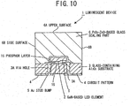
- Fig. 10 is a longitudinal sectional view showing a second variant of the luminescent device in the fourth embodiment.
- This luminescent device 1 is different from the device in the fourth embodiment in that a phosphor-containing phosphor layer 15 is provided so as to cover the whole periphery of the GaN-based LED element 2 .
- the phosphor layer 15 comprises a YAG-based phosphor as a phosphor mixed in the element coating material 14 made of a SiO 2 -based coating material used in the first variant.
- a single type of phosphor or plural types of phosphors may be mixed in the element coating material 14 .
- Other phosphors usable herein include silicate phosphors. Further, a mixture of the YAG-based phosphor with the silicate phosphor may be contained in the phosphor layer 15 .
- an additional effect can be attained. Specifically, since the phosphor is shielded from external moisture by glass sealing, a deterioration of the phosphor can be prevented, and stable wavelength conversion can be realized for a long period of time.
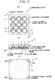
- Fig. 11 shows a luminescent device in the fifth embodiment, wherein (a) is a plan view of the luminescent device, (b) a side view of the luminescent device, and (c) a bottom view of the luminescent device.
- This luminescent device 1 includes a plurality of flip chip-type GaN-based LED elements 2 , a squarely formed glass-containing Al 2 O 3 substrate 3 having a multilayered structure with the GaN-based LED elements 2 mounted thereon, a circuit pattern 4 , made of tungsten (W) provided on the surface of the glass-containing Al 2 O 3 substrate 3 and within the layers (an Ni, Au plating being further applied on the pattern on the substrate surface), an Au stud bump 5 for electrically connecting the GaN-based LED element 2 to the circuit pattern 4 , a P 2 O 5 -ZnO-based glass sealing part 6 for sealing of the GaN-based LED element 2 and, in addition, bonding to the glass-containing Al 2 O 3 substrate 3 , bottom circuit patterns 16 A (an
- the glass-containing Al 2 O 3 substrate 3 has a multilayered structure with in-layer wiring made of W, and, three GaN-based LED elements 2 in a column-wise direction shown in Fig. 11 (b) are connected in series to form an element group.
- the anode in the element group is connected to one of the bottom circuit patterns 16 A, and the cathode in the element group is connected to the bottom circuit pattern 16 C. Further, to the cathode is connected the cathode in element groups formed for other two columns.
- a series/parallel circuit can easily be formed by using a ceramic multilayered substrate, and, further, in electroplating, drawing of the wiring is also easy. Rapid thermal conduction of heat, produced based on light emission from densely mounted nine GaN-based LED elements 2 , from the heat dissipation metal pattern to a heat sink or the like can be realized by drawing an external electrical connection terminal from the intermediate layer and providing a metal pattern for heat dissipation on the bottom face.
- Fig. 12 is a longitudinal sectional view showing a first variant of the luminescent device in the fifth embodiment.
- This luminescent device 1 is different from the device in the fifth embodiment in that a phosphor layer 15 is provided on the surface of the P 2 O 5 -ZnO-based glass sealing part 6 to constitute a wavelength conversion-type luminescent device 1 .
- the provision of the phosphor layer 15 surrounding the whole GaN-based LED element 2 in the P 2 O 5 -ZnO-based glass sealing part 6 can realize a highlight output white luminescent device 1 . Further, even though there is a variation in individual LED element characteristics in the multi-element-type luminescent device 1 , the difference is less likely to be conspicuous and, thus, a luminescent device 1 having uniform luminescent characteristics can be realized.
- Fig. 13 is a longitudinal sectional view showing a second variant of the luminescent device in the fifth embodiment.
- This luminescent device 1 is different from the device in the fifth embodiment in that a blue or green light emitting flip chip-type GaN-based LED element 2 and a red light emitting upper/lower electrode-type AlInGaP-based LED element 2 are provided together followed by sealing by a P 2 O 5 -ZnO-based glass sealing part 6.
- the AlInGaP-based LED element 2 together with the wire 10 , is surrounded by the heat resistant inorganic material coating 11 .
- the flip chip-type LED element and the upper/lower electrode-type LED element are provided together, glass sealing by the P 2 O 5 -ZnO-based low melting glass is possible.
- a combination of luminescent colors of the LED elements 2 may also be desirably set.
- Fig. 14 is a cross-sectional view of a luminescent device in the sixth embodiment.
- This luminescent device 1 includes an AlInGaP-based LED element 2 having an-electrode on its upper and lower parts, a glass-containing Al 2 O 3 substrate 3 with the AlInGaP-based LED element 2 mounted thereon, a circuit pattern 4 formed on the glass-containing Al 2 O 3 substrate 3 made of W, an Au wire 10 for electrically connecting the AlInGaP-based LED element 2 in its electrode to the circuit pattern 4 , a high refractive index material coating 11 A of TiO 2 (refractive index: 2.4 ) for surrounding and coating the AlInGaP-based LED element 2 , the wire 10 , and the circuit pattern 4 , an Ag paste 13 for bonding and electrically connecting the AlInGaP-based LED element 2 to the circuit pattern 4 , and an SiO 2 -Nb 2 O 5 -based glass sealing part 6 for sealing the AlInGaP-based LED element 2 and bonded to
- the SiO 2 -Nb 2 O 5 -based glass sealing part 6 is made of SiO 2 -Nb 2 O 5 -based low melting glass (coefficient of thermal expansion: 10.2 ⁇ 10 -6 /°C, yield point: 543 °C, refractive index: 1.92 , internal transmittance: 81% ( 470 nm), 91 % ( 520 nm (in thickness 10 mm))) and has a semisphericl optical shape face 6 D.
- the optical shape face 6 D may be of a form other than the semisphere so far as light emitted from the AlInGaP-based LED element 2 enters at a critical angle or less to the interface of the glass sealing part 6. Specifically, the optical shape face 6 D may be in a hexahedron or octahedron form.
- the AlInGaP-based LED element 2 is surrounded by the high refractive index material coating 11 A made of TiO 2 with a refractive index of 2.4 and is sealed by the SiO 2 -Nb 2 O 5 -based glass sealing part 6 having a refractive index of 1.92 . Therefore, the occurrence of interface reflection loss at the interface of the high refractive index material coating 11 A and the SiO 2 -Nb 2 O 5 -based glass sealing part 6 can be suppressed, and the efficiency of takeout of light from the LED element as the high refractive index medium can be improved.
- the SiO 2 -Nb 2 O 5 -based glass sealing part 6 is formed in a convex form, light emitted from the AlInGaP-based LED element 2 enters the interface of the glass sealing part 6 and the air at an angle corresponding to near vertical incidence, resulting in enhanced external radiation efficiency.
- Fig. 15 shows a first variant of the luminescent device in the sixth embodiment, wherein (a) is a longitudinal sectional view of the luminescent device and (b) a side view of a GaN-based LED element as a light source.
- This luminescent device 1 is different from the device in the sixth embodiment in that a GaN-based LED element 2 provided with an SiC substrate 29 is used instead of the AlInGaP-based LED element 2 and, further, an optical shape face 6 D made of an SiO 2 film 6 E having a quarter-wavelength thickness is provided on the surface of the SiO 2 -Nb 2 O 5 -based glass sealing part 6.
- the SiC substrate 29 has on its bottom face an n-electrode 26 which is electrically connected to the circuit pattern 4 through an Ag paste 13 .
- the provision of the SiO 2 film 6 E having a quarter-wavelength thickness on the optical shape face 6 D can reduce reflection because light led to the optical shape face 6 D interferes in the SiO 2 film 6 E.
- Fig. 16 shows a second variant of the luminescent device in the sixth embodiment, wherein (a) is a longitudinal sectional view of the luminescent device and (b) a side view of a GaN-based LED element as a light source.
- This luminescent device 1 is different from the device in the sixth embodiment in that a flip chip-type GaN-based LED element 2 provided with a GaN substrate 30 is used instead of the AlInGaP-based LED element 2 .
- the GaN-based LED element 2 provided with the GaN substrate 30 , light can be efficiently led to the substrate surface without interface reflection within the LED element.
- the light led to the surface of the substrate is radiated to the exterior of the device from the optical shape face 6 D through the SiO 2 -Nb 2 O 5 -based glass sealing part 6 , whereby high external radiation efficiency can be realized.
- Fig. 17 shows a luminescent device in the seventh embodiment, wherein (a) is a longitudinal sectional view of the luminescent device and (b) a side view of a GaN-based LED element as a light source.
- This luminescent device 1 is different from the devices in the first to sixth embodiments in that, instead of the glass-containing Al 2 O 3 , Al 2 O 3 is used as the substrate and a sealing glass material corresponding to the coefficient of thermal expansion of Al 2 O 3 is used.
- Fig. 17 illustrates the state before splitting into individual devices. As shown in Fig.
- each of the luminescent devices 1 includes a flip chip-type GaN-based LED element 2 , an Al 2 O 3 substrate 3 with the GaN-based LED element 2 mounted thereon, a circuit pattern 4 provided on the Al 2 O 3 substrate 3 , an Au stud bump 5 for electrically connecting the GaN-based LED element 2 to the circuit pattern 4 , and a B 2 O 3 -F-based glass sealing part 6 for sealing the GaN-based LED element 2 and bonded to the Al 2 O 3 substrate 3 .
- underfilling 7 is filled into a part between the GaN-based LED element 2 and the Al 2 O 3 substrate 3 .
- the Al 2 O 3 substrate 3 has via holes 3 A, and the circuit pattern 4 on the surface is electrically connected to the circuit pattern 4 on the backside through the via holes 3 A.
- Grooves 3 B as a substrate splitting position are formed at predetermined intervals.
- bonding patterns 4 A, 4 B for enhancing the strength of bonding to the B 2 O 3 -F-based glass sealing part 6 are provided on the surface on which the GaN-based LED element 2 is to be mounted, and the bonding pattern 4 B serves also as a part of the circuit pattern 4 drawn out to the backside of the Al 2 O 3 substrate 3 .
- the B 2 O 3 -F-based glass sealing part 6 is made of B 2 O 3 -F-based low melting glass (coefficient of thermal expansion: 6.9 ⁇ 10 -6 /°C, yield point: 539 °C, refractive index: 1.75 , internal transmittance: 98 % ( 470 nm)) and is bonded to the surface of the Al 2 O 3 substrate 3 by hot pressing a preform glass on which an optical shape face 6 D and a small thickness part 6 B have previously been provided by preforming.
- the small thickness part 6 B is formed in such a thickness that damage such as cracking does not extend to the adjacent luminescent device 1 upon the application of a load to scribing part for splitting.
- the GaN-based LED element 2 is mounted and sealed by the B 2 O 3 -F-based glass sealing part 6 , a load is applied using the groove 3 B in the Al 2 O 3 substrate 3 as the splitting position, whereby the Al 2 O 3 substrate 3 is broken based on stress concentration and, at the same time, the B 2 O 3 -F-based glass sealing part 6 is split at the small thickness part 6 B.
- the use of a commonly widely used Al 2 O 3 substrate can reduce white light absorption and can improve light takeout efficiency. Further, the Al 2 O 3 substrate is easily available and is inexpensive. Furthermore, since splitting into individual luminescent devices 1 is carried out by applying a load to the scribing part, mass productivity is excellent. In the splitting into individual luminescent devices 1 by dicing, upon cutting by a dicer, residual stain occurs in the glass and, consequently, cracking sometimes occurs in the B 2 O 3 -F-based glass sealing part 6 upon exposure to heat shock. On the other hand, in the luminescent device 1 split based on scribing, residual strain is small and, thus, a failure such as cracking is less likely to occur.
- SiO 2 -B 2 O 3 -La 2 O 3 -based low melting glass (coefficient of thermal expansion: 8.3 ⁇ 10 -6 /°C, yield point: 559° C, refractive index: 1.81, internal transmittance: 9 9 % ( 470 nm)) may also be used as low melting glass other than the B 2 O 3 -F-based glass.
- splitting using a laser beam may also be adopted.
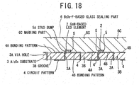
- Fig. 18 is a longitudinal sectional view showing a first variant of the luminescent device in the seventh embodiment.
- This luminescent device 1 is different from the device in the seventh embodiment in that the B 2 O 3 -F-based glass sealing part 6 is formed by flat B 2 O 3 -F-based low melting glass.
- the B 2 O 3 -F-based SiO 2 -B 2 O 3 glass sealing part 6 has a scribing part 6 C at a position opposite to the groove 3 B provided in the Al 2 O 3 substrate 3 , and, upon the application of a load, the scribing part 6 C cooperates with the groove 3 B to cause stress concentration, whereby the B 2 O 3 -F-based glass sealing part 6 and the Al 2 O 3 substrate 3 are split.
- the first variant renders the preform of the B 2 O 3 -F-based glass sealing part 6 unnecessary to simplify the manufacturing process, contributing to excellent productivity.
- SiO 2 -B 2 O 3 -based low melting glass can also be used as other low melting glass applicable to the glass sealing part 6.
- Fig. 19 is a luminescent device of the eighth embodiment, wherein (a) is a longitudinal sectional view of the luminescent device and (b) a side view of a GaN-based LED element as a light source.
- This luminescent device 1 is different from the device in the seventh embodiment in that this device is provided with BN underfilling 7 having excellent thermal conductivity on the lower part of the GaN-based LED element 2 , an AlN substrate 3 with the GaN-based LED element 2 mounted thereon, and an SiO 2 -B 2 O 3 -based glass sealing part 6, having a coefficient of thermal expansion similar to AlN, for sealing the GaN-based LED element 2 and bonded to the AlN substrate 3 .
- the SiO 2 -B 2 O 3 -based glass sealing part 6 is made of SiO 2 -B 2 O 3 -based low melting glass (coefficient of thermal expansion: 4.9 ⁇ 10 -6 /°C, yield point: 558 °C, refractive index: 1.61 , internal transmittance: 96 % ( 380 nm)) and has a coefficient of thermal expansion substantially equal to the coefficient of thermal expansion ( 5 ⁇ 10 -6 /°C) of the GaN-based LED element 2 .
- heat produced based on light emission from the GaN-based LED element 2 is passed through highly thermally conductive unerfilling 7 and Au stud bump 5 , is conveyed to the AlN substrate 3 as a high heat dissipation material and is then efficiently dissipated to the outside of the device. Further, since main members such as the GaN-based LED element 2 , the AlN substrate 3 , and the SiO 2 -B 2 O 3 -based glass sealing part 6 are substantially equal to one another in coefficient of thermal expansion, separation and deterioration in sealing properties derived from the difference in coefficient of thermal expansion can be prevented.
- the provision of a construction capable of relaxing the stress can absorb the internal stress and can prevent deterioration in sealing properties and separation.
- Fig. 20 is a longitudinal sectional view showing a variant of the luminescent device in the eighth embodiment.
- This luminescent device 1 is different from the device in the seventh embodiment in that a soft metal layer for absorbing the internal stress is provided on the surface of the GaN-based LED element 2 mounted circuit pattern 4 .
- Figs. 21 (a) to (e) are diagrams showing a process for forming a circuit pattern on the AlN substrate.
- a W-containing paste is screen printed according to the circuit pattern on both sides of the AlN substrate 3 with via holes 3 A previously formed therein.
- the AlN substrate 3 is sintered at a temperature above 1500° C to bake W to the AlN substrate 3 .
- W is strongly bonded to the AlN substrate 3 .
- W may be formed by sputtering.
- a high melting metal such as Mo may be used.
- a nickel (Ni) layer 26 is provided by plating on the circuit pattern 4 on the surface side of the AlN substrate 3 .
- the AlN substrate 3 is heated at about 700 °C to react Ni with W.
- the circuit pattern 4 is strongly bonded onto the AlN substrate 3 .
- an Au layer 4 C is formed by electroplating on the surface of the circuit pattern 4 .
- the GaN-based LED element 2 is then mounted at a predetermined position through an Au stud bump 5 .
- SiO 2 -B 2 O 3 -based low melting glass is hot pressed on the AlN substrate 3 with the GaN-based LED element 2 mounted on the circuit pattern 4 , followed by splitting into individual luminescent devices 1 based on scribing.
- the strong circuit pattern 4 can be bonded to the AlN substrate 3. Further, the provision of the Au pattern 4 C for mounting the GaN-based LED element 2 on the circuit pattern 4 through the Au stud bump and the provision of the Ni pattern 4 A for bonding to the low melting glass can realize stud bump mounting and, at the same time, can relax stress. In the glass, bonding is carried out through an oxide, and bonding to Au does not occur, but on the other hand, bonding to Ni takes place through an Ni oxide film on the Ni surface. Further, good bonding can also be realized between the glass and AlN.
- the thermal conductivity of the AlN substrate is so high that a difference in temperature between the AlN substrate and the glass is likely to occur, for example, immediately after lighting of the GaN-based LED element 2 . Even in such a situation, stable glass sealing properties can be realized as a result of stress relaxation based on the elastic deformation of the Au layer 4 C can be provided.
- Fig. 22 is a longitudinal sectional view of a luminescent device in the ninth embodiment.
- This luminescent device 1 includes a flip chip-type GaN-based LED element 2 , an AlN submount 18 on which the GaN-based LED element 2 is mounted, a W circuit pattern 4 formed on the AlN submount 18 , a lead 19 made of a copper alloy having a stepped part 19 A on which the AlN submount 18 is mounted, an Au stud bump 5 for electrically connecting the GaN-based LED element 2 to the circuit pattern 4 , and a P 2 O 5 -F-based glass sealing part 6 for surrounding and integrally sealing the GaN-based LED element 2 and the lead 19 .
- the AlN submount 18 has a metallized circuit pattern.
- the P 2 O 5 -F-based glass sealing part 6 is made of P 2 O 5 -F-based low melting glass (coefficient of thermal expansion: 16.9 ⁇ 10 -6 /°C, yield point: 363 °C, refractive index: 1.54 , internal transmittance: 99 % ( 470 nm)), and an optical shape face 6 D, which is formed in a semispherical form and functions to radiate light to a desired radiation range, is formed based on hot pressing.
- Two P 2 O 5 -F-based low melting glass sheets are set parallel to each other so as to sandwich a lead 19 , formed in the lead frame, therebetween, and the assembly is hot pressed in a nitrogen atmosphere under conditions of pressure 10 kgf and temperature 410 °C or above. Under the above conditions, the viscosity of the low melting glass is 10 8 to 10 9 poises.
- Fig. 23 is a diagram illustrating the state of glass sealing of the lead frame by hot pressing.
- a lead frame 31 is shown in which a pair of leads 311 made of a copper alloy sheet are led out in a single direction.
- This lead frame 31 includes a lead 311 for fixing an AlN submount 18 , an opening 312 provided on the support side of the lead 311 , an oval hole 313 for absorbing thermal deformation of the lead frame 31 , and a positioning hole 314 for positioning the feed position of the lead frame 31 .
- the periphery of the lead 311 is removed as an opening 310 in punching out the copper alloy sheet.
- the method for manufacturing the luminescent device 1 will be explained.
- a lead frame 31 with a lead 19 having a stepped part 19 A for mounting the AlN submount 18 is first formed.
- An AlN submount 18 with a circuit pattern 4 formed thereon is then bonded to the lead frame 31 .
- a GaN-based LED element 2 is bonded by flip chip binding through an Au stud bump 5 to the circuit pattern 4 provided on the surface of the AlN submount 18 .
- P 2 O 5 -F-based low melting glass is set parallel to each other on and under the lead frame 31 . The P 2 O 5 -F-based low melting glass is then hot pressed using a mold (not shown).
- the P 2 O 5 -F-based low melting glass is molded individually in the small thickness part 6 B and the P 2 O 5 -F-based glass sealing part 6 based on hot pressing.
- the lead 311 is cut for isolation of luminescent devices from the lead frame 31.
- the material for constituting the submount is not limited to AlN and may be sapphire (Al 2 O 3 ).
- Al 2 O 3 the difference in coefficient of thermal expansion between Al 2 O 3 and the glass material is small and, thus, the occurrence of cracking and separation can be suppressed.
- a construction may be adopted in which a GaN-based LED element 2 is loaded on a Si submount 18 which functions as a Zener diode by an n layer 18B and a p layer 18C.
- the GaN-based LED element can be protected against electrostatic discharge damage.
- damage caused by glass sealing can be avoided by protection with a protecting member such as the above-described heat resistant inorganic material coating 11.
- white glass may be used on the lower side.
- light emitted to the lower side can be reflected and radiated to the optical shape formation side.
- the two glass sheets for sandwiching the lead therebetween may be different from each other in viscosity.
- P 2 O 5 -F-based low melting glass coefficient of thermal expansion: 17.3 ⁇ 10 -6 /°C, yield point: 310° C, refractive index: 1.51, internal transmittance: 99 % ( 470 nm)
- P 2 O 5 -F-based low melting glass coefficient of thermal expansion: 16.9 ⁇ 10 -6 /°C, yield point: 363°C, refractive index: 1.54, internal transmittance: 99% ( 470 nm)
- the upper side is higher viscosity
- the lower side is lower viscosity. This facilitates molding.
- Fig. 25 is a luminescent device in a first example not forming part of the present invention, wherein (a) is a plan view, (b) a cross-sectional view taken on line A-A of (a), and (c) a perspective view of the lower glass.
- This luminescent device 1 includes a face up-type GaN-based LED element 2 , a lead 19 having a lead cup part 19 B on which the GaN-based LED element 2 is mounted, a wire 10 for electrically connecting the GaN-based LED element 2 to the lead 19 , a silicone coating 35 for covering and protecting the GaN-based LED element 2 and the wire 10 , and a P 2 O 5 -F-based glass sealing part 6 for integrally sealing the lead 19 through the preformed upper glass 60 A and lower glass 60 B.
- the lead cup part 19 B is provided in a cone form by an inclined face 190 and a bottom face 191 and is received in a lead receiving groove 60 C of the lower glass 60 B shown in (c).
- the lead receiving groove 60 C is formed in preforming the lower glass 60 B using a mold.
- the method for manufacturing the first example of the luminescent device 1 will be explained.
- a lead frame (not shown) of copper provided with a pair of leads 19 having a silver plated surface is provided.
- a GaN-based LED element 2 is mounted on the lead 19 in its lead cup part 19 B.
- the GaN-based LED element 2 is bonded to the lead cup face 19 B on its bottom face 191 .
- the pair of leads 19 are then electrically connected to the GaN-based LED element 2 on its electrode through a wire 10 .
- the assembly is received in the lead receiving groove 60 C in the preformed lower glass 60 B.
- a silicone resin coating 35 is then potted so as to cover the pair of leads 19 and the GaN-based LED element 2 .
- the upper glass 60 A is then provided and is integrated with the lower glass 60 B based on hot pressing.
- the luminescent device 1 is cut out from the lead frame.
- the molecular bond is cleaved by heat at about 400 °C or above, and, consequently, gas is evolved. Since the silicone resin coating 35 can be processed at 360 °C without heat decomposition, heat applied during the glass sealing can be absorbed in the silicone resin to relax the stress. Further, the use of the preformed lower glass 60 B for receiving the lead cup part 19 B can stabilize glass sealing state of the pair of leads 19 . A large quantity of luminescent devices can be manufactured at a time by conducting hot pressing to the lead frame for individual glass sealing of leads and conducting tie bar cutting from the lead frame, and, thus, excellent mass productivity can be realized.
- Fig. 26 is a cross-sectional view showing a first variant of the luminescent device in the first example, not forming part of the present invention.
- This luminescent device 1 is different from the device in the first example in that the luminescent device 1 includes a flip chip-type GaN-based LED element 2 ( 0.3 mm ⁇ 0.3 mm), an AlN submount 18 on which the GaN-based LED element 2 is mounted, and a pair of lead frames 19 having a stepped part 19 A for receiving the AlN submount 18 .
- the pair of lead frames 19 has an inclined face 19 D above the stepped part 19 A, and light emitted from the GaN-based LED element 2 is reflected from the inclined face 19 D for external radiation.
- the AlN submount 18 has via holes 18 A for electrically connecting the circuit pattern 4 provided on the surface to the circuit pattern 4 provided on the backside.
- a lead frame (not shown) provided with a pair of leads 19 is first provided.
- an AlN submount 18 is electrically connected through an Ag paste so as to be located in a stepped part 19 A in the lead 19 .
- a GaN-based LED element 2 is then bonded to the AlN submount 18 through an Au stud bump 5 .
- the assembly is then received in the lead receiving groove 60 C of the preformed lower glass 60 B.
- a silicone coating 35 is potted so as to cover the pair of leads 19 and the GaN-based LED element 2 .
- An upper glass 60 A is then provided and is integrated with a lower glass 60 B by hot pressing. The luminescent device 1 is then cut out from the lead frame.
- light can be efficiently taken out from the substrate side by using the flip chip-type GaN-based LED element 2 .
- Fig. 27 is a cross-sectional view of a second variant of the luminescent device in the first example, not forming part of the present invention.
- This luminescent device 1 is different from the device in the first example in that the luminescent device 1 includes a flip chip-type GaN-based LED element (large size) 2 , an AlN submount 18 on which the GaN-based LED element 2 is mounted, and a pair of lead frames 19 having a stepped part 19 A for receiving the AlN submount 18 .
- the size of the large-size GaN-based LED element 2 is 1 mm ⁇ 1 mm.
- the construction using a large-size chip has been explained. Since the chip size is large, the difference in coefficient of thermal expansion between the P 2 O 5 -F-based glass AlN submount 18 and the P 2 O 5 -F-based glass sealing part 6 is large. Even in this case, good sealing properties are obtained.
- Fig. 28 shows a luminescent device in a second example not forming part of the present invention, wherein (a) is a side view and (b) a perspective view illustrating glass sealing.
- a tubular body 60 D made of P 2 O 5 -F-based glass is heated to glass-seal the GaN-based LED element 2 , the wire 10 , and the pair of leads 19 .
- the tubular body 60 D is formed of a partially cut-out tubular glass.
- the tubular body 60 D is heated by a heating device such as a burner (not shown) to melt the glass for glass sealing of the GaN-based LED element 2 , the wire 10 , and the pair of leads 19 .
- the GaN-based LED element 2 , the wire 10 , and the pair of leads 19 can be glass-sealed based on the surface tension of the melted glass.
- glass sealing is carried out by depositing the melted glass.
- hot pressing may be carried out in such a state that the glass is in a melted state.
- Fig. 29 is a longitudinal sectional view of a luminescent device in the tenth embodiment.
- This luminescent device 1 is different from the luminescent device 1 in the ninth embodiment in that a mold part 9 made of an epoxy resin is provided.
- the mold part 9 has a semispherical optical shape face 9 A and is formed by transfer molding.
- an optical system can easily be formed in the glass sealing-type device, and, at the same time, the moisture resistance is further improved by surrounding the glass sealing part 6 by the mold part 9 .
- the lead-out part is not directly from the glass, and, thus, cracking or breaking of glass caused by stress or the like at the time of bending of the lead can be advantageously prevented.
- the mold part 9 may be made of other resin material other than the epoxy resin, for example, a silicone resin, and molding methods other than transfer molding, for example, potting molding, can also be applied.
- the mold part 9 may be formed by an injection method using a resin material such as acrylic or polycarbonate resin, and, in this case, the productivity can be improved.
- sealing of the element with a sealing material with a refractive index of about 1.5 or more can enhance the efficiency of takeout of light from the element by about twice or more.
- the sealing material should be transparent to light. In photodetectors, this effect cannot be attained, and the effect attained by intimate contact sealing of the element directly with the light transparent material is only the effect of reducing reflection at interface between dissimilar media.
Landscapes
- Chemical & Material Sciences (AREA)
- Engineering & Computer Science (AREA)
- Geochemistry & Mineralogy (AREA)
- Life Sciences & Earth Sciences (AREA)
- Chemical Kinetics & Catalysis (AREA)
- General Chemical & Material Sciences (AREA)
- Materials Engineering (AREA)
- Organic Chemistry (AREA)
- Ceramic Engineering (AREA)
- Led Device Packages (AREA)
- Led Devices (AREA)
- Glass Compositions (AREA)
- Encapsulation Of And Coatings For Semiconductor Or Solid State Devices (AREA)
Claims (3)
- Procédé de fabrication d'un dispositif à élément solide (1) comprenant un élément optique (2) scellé avec un matériau de verre, ledit procédé comprenant :une étape de montage d'une pluralité d'éléments optiques (2) sur une partie de réception et de fourniture d'alimentation électrique comprenant un substrat de matériau inorganique (3) ayant un côté de surface et un côté arrière, ladite pluralité d'éléments optiques (2) étant montée sur ledit côté de surface, et une électrode (4) étant formée et sortant au niveau dudit côté arrière ;une étape de scellement consistant à lier un matériau de verre à ladite surface dudit substrat de matériau inorganique (3), en scellant ainsi ladite pluralité d'éléments optiques (2) avec ledit matériau de verre ; etune étape d'isolation consistant à isoler ladite partie de réception et de fourniture d'alimentation électrique comprenant ledit substrat de matériau inorganique (3) intégré audit matériau de verre dans une pluralité de dispositifs à élément solide (1),caractérisé en ce queladite étape de scellement inclut la compression d'un verre préformé contre ladite surface dudit substrat de matériau inorganique (3) dans une atmosphère barrière à l'oxygène à une température supérieure ou égale à un point de déformation dudit verre préformé pour réaliser ladite liaison et ledit scellement.
- Procédé de fabrication d'un dispositif à élément solide (1) selon la revendication 1, dans lequel :
ladite étape de montage est opérée par montage par retournement. - Procédé de fabrication d'un dispositif à élément solide (1) selon la revendication 1, dans lequel :
ladite étape de scellement est opérée de telle sorte que ledit verre préformé est traité dans des conditions de haute viscosité d'au moins 105 Pa.s (106 poises).
Applications Claiming Priority (9)
| Application Number | Priority Date | Filing Date | Title |
|---|---|---|---|
| JP2003063015 | 2003-03-10 | ||
| JP2003160855 | 2003-06-05 | ||
| JP2003160867A JP2006086138A (ja) | 2003-06-05 | 2003-06-05 | 光デバイス |
| JP2003193182A JP2006086139A (ja) | 2003-07-07 | 2003-07-07 | 発光装置 |
| JP2003342705A JP4303550B2 (ja) | 2003-09-30 | 2003-09-30 | 発光装置 |
| JP2003342706A JP4016925B2 (ja) | 2003-09-30 | 2003-09-30 | 発光装置 |
| JP2004010385A JP4029843B2 (ja) | 2004-01-19 | 2004-01-19 | 発光装置 |
| PCT/JP2004/003089 WO2004082036A1 (fr) | 2003-03-10 | 2004-03-10 | Dispositif a element solide et son procede de production |
| EP04719060.8A EP1603170B1 (fr) | 2003-03-10 | 2004-03-10 | Procédé de production d'un dispositif à élément optique dans l'état-solide |
Related Parent Applications (3)
| Application Number | Title | Priority Date | Filing Date |
|---|---|---|---|
| EP04719060.8 Division | 2004-03-10 | ||
| EP04719060.8A Division EP1603170B1 (fr) | 2003-03-10 | 2004-03-10 | Procédé de production d'un dispositif à élément optique dans l'état-solide |
| EP04719060.8A Division-Into EP1603170B1 (fr) | 2003-03-10 | 2004-03-10 | Procédé de production d'un dispositif à élément optique dans l'état-solide |
Publications (3)
| Publication Number | Publication Date |
|---|---|
| EP2596948A2 EP2596948A2 (fr) | 2013-05-29 |
| EP2596948A3 EP2596948A3 (fr) | 2017-03-15 |
| EP2596948B1 true EP2596948B1 (fr) | 2020-02-26 |
Family
ID=32996669
Family Applications (2)
| Application Number | Title | Priority Date | Filing Date |
|---|---|---|---|
| EP13156568.1A Expired - Lifetime EP2596948B1 (fr) | 2003-03-10 | 2004-03-10 | Procédé pour la fabrication d'un dispositif semiconducteur |
| EP04719060.8A Expired - Lifetime EP1603170B1 (fr) | 2003-03-10 | 2004-03-10 | Procédé de production d'un dispositif à élément optique dans l'état-solide |
Family Applications After (1)
| Application Number | Title | Priority Date | Filing Date |
|---|---|---|---|
| EP04719060.8A Expired - Lifetime EP1603170B1 (fr) | 2003-03-10 | 2004-03-10 | Procédé de production d'un dispositif à élément optique dans l'état-solide |
Country Status (6)
| Country | Link |
|---|---|
| US (3) | US7824937B2 (fr) |
| EP (2) | EP2596948B1 (fr) |
| KR (1) | KR100693969B1 (fr) |
| CN (2) | CN101789482B (fr) |
| TW (1) | TWI246780B (fr) |
| WO (1) | WO2004082036A1 (fr) |
Families Citing this family (333)
| Publication number | Priority date | Publication date | Assignee | Title |
|---|---|---|---|---|
| US7550777B2 (en) * | 2003-01-10 | 2009-06-23 | Toyoda Gosei, Co., Ltd. | Light emitting device including adhesion layer |
| CN101789482B (zh) * | 2003-03-10 | 2013-04-17 | 丰田合成株式会社 | 固体元件装置及其制造方法 |
| JP4029843B2 (ja) * | 2004-01-19 | 2008-01-09 | 豊田合成株式会社 | 発光装置 |
| US10686106B2 (en) | 2003-07-04 | 2020-06-16 | Epistar Corporation | Optoelectronic element |
| US9142740B2 (en) | 2003-07-04 | 2015-09-22 | Epistar Corporation | Optoelectronic element and manufacturing method thereof |
| US9000461B2 (en) * | 2003-07-04 | 2015-04-07 | Epistar Corporation | Optoelectronic element and manufacturing method thereof |
| US20050116235A1 (en) * | 2003-12-02 | 2005-06-02 | Schultz John C. | Illumination assembly |
| JP2006066868A (ja) | 2004-03-23 | 2006-03-09 | Toyoda Gosei Co Ltd | 固体素子および固体素子デバイス |
| JP5141608B2 (ja) * | 2004-03-23 | 2013-02-13 | 豊田合成株式会社 | 固体素子デバイスの製造方法 |
| JPWO2005114730A1 (ja) * | 2004-05-20 | 2008-03-27 | スパンション エルエルシー | 半導体装置の製造方法および半導体装置 |
| JP2006100787A (ja) | 2004-08-31 | 2006-04-13 | Toyoda Gosei Co Ltd | 発光装置および発光素子 |
| JP4630629B2 (ja) * | 2004-10-29 | 2011-02-09 | 豊田合成株式会社 | 発光装置の製造方法 |
| JP4394036B2 (ja) * | 2004-09-09 | 2010-01-06 | 豊田合成株式会社 | 固体素子デバイス |
| JP4747726B2 (ja) | 2004-09-09 | 2011-08-17 | 豊田合成株式会社 | 発光装置 |
| US7842526B2 (en) | 2004-09-09 | 2010-11-30 | Toyoda Gosei Co., Ltd. | Light emitting device and method of producing same |
| JP4747704B2 (ja) * | 2005-07-20 | 2011-08-17 | 豊田合成株式会社 | 蛍光体層付き発光装置の製造方法 |
| US7470926B2 (en) * | 2004-09-09 | 2008-12-30 | Toyoda Gosei Co., Ltd | Solid-state optical device |
| US7417220B2 (en) * | 2004-09-09 | 2008-08-26 | Toyoda Gosei Co., Ltd. | Solid state device and light-emitting element |
| JP2006086469A (ja) * | 2004-09-17 | 2006-03-30 | Matsushita Electric Ind Co Ltd | 半導体発光装置、照明モジュール、照明装置及び半導体発光装置の製造方法 |
| US7745832B2 (en) * | 2004-09-24 | 2010-06-29 | Epistar Corporation | Semiconductor light-emitting element assembly with a composite substrate |
| DE102004050371A1 (de) | 2004-09-30 | 2006-04-13 | Osram Opto Semiconductors Gmbh | Optoelektronisches Bauelement mit einer drahtlosen Kontaktierung |
| US7419839B2 (en) | 2004-11-12 | 2008-09-02 | Philips Lumileds Lighting Company, Llc | Bonding an optical element to a light emitting device |
| US7344902B2 (en) | 2004-11-15 | 2008-03-18 | Philips Lumileds Lighting Company, Llc | Overmolded lens over LED die |
| US7714335B2 (en) * | 2004-11-19 | 2010-05-11 | Koninklijke Philips Electronics N.V. | Light-emitting device with inorganic housing |
| JP2006156668A (ja) * | 2004-11-29 | 2006-06-15 | Nichia Chem Ind Ltd | 発光装置及びその製造方法 |
| US20090273727A1 (en) * | 2004-12-03 | 2009-11-05 | Sony Corporation | Light-emission lens, light-emitting element assembly, sheet-shaped light source device and color liquid crystal display assembly |
| KR100867515B1 (ko) * | 2004-12-06 | 2008-11-07 | 삼성전기주식회사 | 발광소자 패키지 |
| TWI420686B (zh) * | 2004-12-10 | 2013-12-21 | 松下電器產業股份有限公司 | 半導體發光裝置、發光模組及照明裝置 |
| WO2006098545A2 (fr) * | 2004-12-14 | 2006-09-21 | Seoul Opto Device Co., Ltd. | Dispositif electroluminescent comprenant une pluralite de cellules electroluminescentes, et boitier de support pour ce dispositif |
| TWI317829B (en) * | 2004-12-15 | 2009-12-01 | Epistar Corp | Led illumination device and application thereof |
| JP2006179572A (ja) * | 2004-12-21 | 2006-07-06 | Sharp Corp | 発光ダイオード、バックライト装置および発光ダイオードの製造方法 |
| TWI374553B (en) * | 2004-12-22 | 2012-10-11 | Panasonic Corp | Semiconductor light emitting device, illumination module, illumination apparatus, method for manufacturing semiconductor light emitting device, and method for manufacturing semiconductor light emitting element |
| KR100862457B1 (ko) * | 2004-12-29 | 2008-10-08 | 삼성전기주식회사 | 금속컬럼을 이용한 발광소자의 플립칩 본딩 구조체 |
| JP5109226B2 (ja) * | 2005-01-20 | 2012-12-26 | 豊田合成株式会社 | 発光装置 |
| JP4492378B2 (ja) * | 2005-02-03 | 2010-06-30 | 豊田合成株式会社 | 発光装置およびその製造方法 |
| US20060171152A1 (en) * | 2005-01-20 | 2006-08-03 | Toyoda Gosei Co., Ltd. | Light emitting device and method of making the same |
| KR101197046B1 (ko) | 2005-01-26 | 2012-11-06 | 삼성디스플레이 주식회사 | 발광다이오드를 사용하는 2차원 광원 및 이를 이용한 액정표시 장치 |
| US7405433B2 (en) | 2005-02-22 | 2008-07-29 | Avago Technologies Ecbu Ip Pte Ltd | Semiconductor light emitting device |
| JP2006245336A (ja) * | 2005-03-03 | 2006-09-14 | Koito Mfg Co Ltd | 発光装置 |
| JP4645240B2 (ja) * | 2005-03-10 | 2011-03-09 | 豊田合成株式会社 | 面状発光装置 |
| EP2280430B1 (fr) * | 2005-03-11 | 2020-01-01 | Seoul Semiconductor Co., Ltd. | Boîtier de diodes électroluminescentes à matrice de cellules photoemettrices montées en serie |
| WO2006112417A1 (fr) * | 2005-04-15 | 2006-10-26 | Asahi Glass Company, Limited | Dispositif electroluminescent sous scellement en verre, carte a circuit imprime avec dispositif electroluminescent sous scellement en verre et leurs procedes de fabrication |
| JP4604819B2 (ja) * | 2005-04-28 | 2011-01-05 | 豊田合成株式会社 | 発光装置 |
| TWI260798B (en) * | 2005-05-02 | 2006-08-21 | Ind Tech Res Inst | Highly heat-dissipating light-emitting diode |
| TWI260800B (en) * | 2005-05-12 | 2006-08-21 | Epitech Technology Corp | Structure of light-emitting diode and manufacturing method thereof |
| JP2006332365A (ja) * | 2005-05-26 | 2006-12-07 | Toyoda Gosei Co Ltd | Iii族窒化物系化合物半導体発光素子およびそれを用いた発光装置 |
| JP4679267B2 (ja) * | 2005-06-29 | 2011-04-27 | シーアイ化成株式会社 | 発光ダイオード複合素子 |
| JP4679268B2 (ja) * | 2005-06-29 | 2011-04-27 | シーアイ化成株式会社 | 発光ダイオード複合素子 |
| DE102005031523B4 (de) * | 2005-06-30 | 2015-11-05 | Schott Ag | Halbleiterlichtquelle mit Lichtkonversionsmedium aus Glaskeramik |
| DE102005038698A1 (de) * | 2005-07-08 | 2007-01-18 | Tridonic Optoelectronics Gmbh | Optoelektronische Bauelemente mit Haftvermittler |
| JP2007027278A (ja) * | 2005-07-13 | 2007-02-01 | Shinko Electric Ind Co Ltd | 半導体装置および半導体装置の製造方法 |
| WO2007013664A1 (fr) * | 2005-07-27 | 2007-02-01 | Showa Denko K.K. | Source de lumière à diodes émettrices de lumière |
| JP2007059894A (ja) * | 2005-07-27 | 2007-03-08 | Showa Denko Kk | 発光ダイオード素子搭載光源 |
| KR100629496B1 (ko) | 2005-08-08 | 2006-09-28 | 삼성전자주식회사 | Led 패키지 및 그 제조방법 |
| US7847302B2 (en) * | 2005-08-26 | 2010-12-07 | Koninklijke Philips Electronics, N.V. | Blue LED with phosphor layer for producing white light and different phosphor in outer lens for reducing color temperature |
| JP2007067300A (ja) * | 2005-09-01 | 2007-03-15 | Asahi Glass Co Ltd | 発光装置およびその製造方法 |
| JP2007073575A (ja) * | 2005-09-05 | 2007-03-22 | Matsushita Electric Ind Co Ltd | 半導体発光装置 |
| JP4961887B2 (ja) * | 2005-09-07 | 2012-06-27 | 豊田合成株式会社 | 固体素子デバイス |
| JP2007080884A (ja) * | 2005-09-09 | 2007-03-29 | Asahi Glass Co Ltd | 発光装置の製造方法、発光装置および発光装置の中間部品 |
| JP2007081234A (ja) | 2005-09-15 | 2007-03-29 | Toyoda Gosei Co Ltd | 照明装置 |
| CN100594623C (zh) * | 2005-09-20 | 2010-03-17 | 松下电工株式会社 | 发光二极管照明器具 |
| JP2007109743A (ja) * | 2005-10-11 | 2007-04-26 | Kaneka Corp | 発光ダイオード |
| JP2009515344A (ja) * | 2005-11-04 | 2009-04-09 | ザ リージェンツ オブ ザ ユニバーシティ オブ カリフォルニア | 高い光抽出効率の発光ダイオード(led) |
| JP2007140179A (ja) * | 2005-11-18 | 2007-06-07 | Seiko Epson Corp | 光モジュールおよびその製造方法 |
| US7728437B2 (en) * | 2005-11-23 | 2010-06-01 | Fairchild Korea Semiconductor, Ltd. | Semiconductor package form within an encapsulation |
| WO2007061033A1 (fr) * | 2005-11-28 | 2007-05-31 | Sharp Kabushiki Kaisha | Dispositif d’éclairage et son procédé de fabrication |
| JP4922607B2 (ja) * | 2005-12-08 | 2012-04-25 | スタンレー電気株式会社 | Led光源装置 |
| JP2007165811A (ja) | 2005-12-16 | 2007-06-28 | Nichia Chem Ind Ltd | 発光装置 |
| JP2007201420A (ja) * | 2005-12-27 | 2007-08-09 | Sharp Corp | 半導体発光装置、半導体発光素子、および半導体発光装置の製造方法 |
| KR100653645B1 (ko) * | 2005-12-27 | 2006-12-05 | 삼성전자주식회사 | 발광소자 패키지 및 발광소자 패키지 제조방법 |
| US7521728B2 (en) * | 2006-01-20 | 2009-04-21 | Cree, Inc. | Packages for semiconductor light emitting devices utilizing dispensed reflectors and methods of forming the same |
| DE112007000290B4 (de) * | 2006-01-31 | 2017-06-14 | Kyocera Corp. | Lichtemittierende Vorrichtung und lichtemittierendes Modul |
| WO2007099796A1 (fr) * | 2006-02-22 | 2007-09-07 | Nippon Sheet Glass Company, Limited. | Unite electroluminescente, dispositif d'eclairage et dispositif de lecture d'image |
| KR100780196B1 (ko) * | 2006-02-27 | 2007-11-27 | 삼성전기주식회사 | 발광다이오드 패키지, 발광다이오드 패키지용 회로기판 및그 제조방법 |
| JP4756349B2 (ja) * | 2006-03-16 | 2011-08-24 | 旭硝子株式会社 | 発光装置の製造方法 |
| DE112007000773B4 (de) * | 2006-03-29 | 2013-04-25 | Kyocera Corp. | Licht emittierende Vorrichtung |
| KR100799864B1 (ko) * | 2006-04-21 | 2008-01-31 | 삼성전기주식회사 | Led 패키지 |
| US7521727B2 (en) * | 2006-04-26 | 2009-04-21 | Rohm And Haas Company | Light emitting device having improved light extraction efficiency and method of making same |
| US7365407B2 (en) * | 2006-05-01 | 2008-04-29 | Avago Technologies General Ip Pte Ltd | Light emitting diode package with direct leadframe heat dissipation |
| US7423297B2 (en) * | 2006-05-03 | 2008-09-09 | 3M Innovative Properties Company | LED extractor composed of high index glass |
| JP5035241B2 (ja) * | 2006-05-18 | 2012-09-26 | 旭硝子株式会社 | 発光装置の製造方法および発光装置 |
| JP4854738B2 (ja) * | 2006-06-15 | 2012-01-18 | 三洋電機株式会社 | 電子部品 |
| KR101314713B1 (ko) * | 2006-06-16 | 2013-10-07 | 신꼬오덴기 고교 가부시키가이샤 | 반도체 장치, 그 제조 방법, 및 기판 |
| KR100809263B1 (ko) * | 2006-07-10 | 2008-02-29 | 삼성전기주식회사 | 직하 방식 백라이트 장치 |
| TWI321857B (en) * | 2006-07-21 | 2010-03-11 | Epistar Corp | A light emitting device |
| JP4930830B2 (ja) * | 2006-07-27 | 2012-05-16 | 日亜化学工業株式会社 | 発光装置 |
| JP5307364B2 (ja) * | 2006-08-03 | 2013-10-02 | 豊田合成株式会社 | 蛍光体含有ガラスの製造方法及び固体素子デバイスの製造方法 |
| KR100866879B1 (ko) * | 2006-12-19 | 2008-11-04 | 엘지전자 주식회사 | 발광 소자 패키지 및 그 제조방법 |
| TWI418054B (zh) | 2006-08-08 | 2013-12-01 | Lg電子股份有限公司 | 發光裝置封裝與製造此封裝之方法 |
| US7439548B2 (en) * | 2006-08-11 | 2008-10-21 | Bridgelux, Inc | Surface mountable chip |
| JP4855869B2 (ja) * | 2006-08-25 | 2012-01-18 | 日亜化学工業株式会社 | 発光装置の製造方法 |
| JP4650378B2 (ja) * | 2006-08-31 | 2011-03-16 | 日亜化学工業株式会社 | 発光装置の製造方法 |
| US20080074574A1 (en) * | 2006-09-09 | 2008-03-27 | Topson Optoelectronics Semi-Conductor Co., Ltd. | Background light module with oval lenses |
| JP4905009B2 (ja) * | 2006-09-12 | 2012-03-28 | 豊田合成株式会社 | 発光装置の製造方法 |
| WO2008035283A2 (fr) | 2006-09-22 | 2008-03-27 | Koninklijke Philips Electronics N.V. | Dispositif luminescent à relâchement de tension |
| DE102007021009A1 (de) * | 2006-09-27 | 2008-04-10 | Osram Opto Semiconductors Gmbh | Leuchtdiodenanordnung und Verfahren zur Herstellung einer solchen |
| US10873002B2 (en) * | 2006-10-20 | 2020-12-22 | Cree, Inc. | Permanent wafer bonding using metal alloy preform discs |
| JP4905069B2 (ja) * | 2006-11-09 | 2012-03-28 | 豊田合成株式会社 | 発光装置及びその製造方法 |
| JP2008124267A (ja) * | 2006-11-13 | 2008-05-29 | Toyoda Gosei Co Ltd | 発光装置 |
| US7964892B2 (en) * | 2006-12-01 | 2011-06-21 | Nichia Corporation | Light emitting device |
| KR100845856B1 (ko) * | 2006-12-21 | 2008-07-14 | 엘지전자 주식회사 | 발광 소자 패키지 및 그 제조방법 |
| CN101257066B (zh) * | 2007-02-28 | 2011-11-23 | 宏齐科技股份有限公司 | 高散热的发光二极管制作方法及其结构 |
| US8610143B2 (en) | 2007-03-12 | 2013-12-17 | Nichia Corporation | High output power light emitting device and package used therefor |
| KR20080085399A (ko) * | 2007-03-19 | 2008-09-24 | 엘지이노텍 주식회사 | Led 모듈 및 이를 구비하는 백라이트 유닛 |
| JP4266234B2 (ja) * | 2007-03-29 | 2009-05-20 | 株式会社東芝 | 半導体発光装置の製造方法 |
| JP5104490B2 (ja) | 2007-04-16 | 2012-12-19 | 豊田合成株式会社 | 発光装置及びその製造方法 |
| EP1983571B1 (fr) | 2007-04-18 | 2019-01-02 | Nichia Corporation | Dispositif luminescent |
| JP2008270563A (ja) * | 2007-04-20 | 2008-11-06 | Toyoda Gosei Co Ltd | 発光装置、光源装置及び発光装置の製造方法 |
| KR20100014822A (ko) | 2007-05-30 | 2010-02-11 | 아사히 가라스 가부시키가이샤 | 광학 소자 피복용 유리, 유리 피복 발광 소자 및 유리 피복 발광 장치 |
| JP5233170B2 (ja) * | 2007-05-31 | 2013-07-10 | 日亜化学工業株式会社 | 発光装置、発光装置を構成する樹脂成形体及びそれらの製造方法 |
| CN101689585A (zh) * | 2007-06-15 | 2010-03-31 | 罗姆股份有限公司 | 半导体发光装置及其制造方法 |
| KR101380385B1 (ko) * | 2007-06-29 | 2014-04-10 | 서울반도체 주식회사 | 일괄 봉지 기술을 이용하는 led 패키지 제조방법 |
| KR20090015734A (ko) | 2007-08-09 | 2009-02-12 | 엘지이노텍 주식회사 | 광원 장치 |
| JP5251038B2 (ja) | 2007-08-23 | 2013-07-31 | 豊田合成株式会社 | 発光装置 |
| JP2009059883A (ja) * | 2007-08-31 | 2009-03-19 | Toyoda Gosei Co Ltd | 発光装置 |
| WO2009031684A1 (fr) * | 2007-09-07 | 2009-03-12 | Asahi Glass Company, Limited | Élément électroluminescent revêtu de verre et dispositif électroluminescent revêtu de verre |
| DE102008005345A1 (de) * | 2007-09-28 | 2009-04-02 | Osram Opto Semiconductors Gmbh | Halbleiterbasiertes Bauelement, Aufnahme für ein halbleiterbasiertes Bauelement und Verfahren zur Herstellung eines halbleiterbasierten Bauelements |
| KR101381762B1 (ko) * | 2007-09-28 | 2014-04-10 | 삼성전자주식회사 | 발광 장치 |
| CN101821867B (zh) * | 2007-10-23 | 2012-01-04 | 松下电器产业株式会社 | 半导体发光器件及使用它的半导体发光装置以及该半导体发光装置的制造方法 |
| TWI358110B (en) * | 2007-10-26 | 2012-02-11 | Lite On Technology Corp | Light emitting diode |
| CN101431132B (zh) * | 2007-11-07 | 2012-04-25 | 光宝科技股份有限公司 | 发光二极管 |
| JP5109620B2 (ja) * | 2007-11-26 | 2012-12-26 | 豊田合成株式会社 | 発光装置、基板装置及び発光装置の製造方法 |
| KR100998233B1 (ko) | 2007-12-03 | 2010-12-07 | 서울반도체 주식회사 | 슬림형 led 패키지 |
| KR100922309B1 (ko) * | 2007-12-12 | 2009-10-21 | 앰코 테크놀로지 코리아 주식회사 | 웨이퍼 레벨 반도체 패키지 제조 방법 |
| JP5311281B2 (ja) * | 2008-02-18 | 2013-10-09 | 日本電気硝子株式会社 | 波長変換部材およびその製造方法 |
| DE102008021436A1 (de) * | 2008-04-29 | 2010-05-20 | Schott Ag | Optik-Konverter-System für (W)LEDs |
| DE102008021435A1 (de) * | 2008-04-29 | 2009-11-19 | Schott Ag | Gehäuse für LEDs mit hoher Leistung |
| CN101587887A (zh) * | 2008-05-23 | 2009-11-25 | 富准精密工业(深圳)有限公司 | 发光二极管结构 |
| KR101438826B1 (ko) * | 2008-06-23 | 2014-09-05 | 엘지이노텍 주식회사 | 발광장치 |
| US8159131B2 (en) * | 2008-06-30 | 2012-04-17 | Bridgelux, Inc. | Light emitting device having a transparent thermally conductive layer |
| TW201011936A (en) * | 2008-09-05 | 2010-03-16 | Advanced Optoelectronic Tech | Light emitting device and fabrication thereof |
| US8008845B2 (en) * | 2008-10-24 | 2011-08-30 | Cree, Inc. | Lighting device which includes one or more solid state light emitting device |
| JP5375041B2 (ja) | 2008-11-13 | 2013-12-25 | 日亜化学工業株式会社 | 発光装置およびその製造方法 |
| TWI380483B (en) * | 2008-12-29 | 2012-12-21 | Everlight Electronics Co Ltd | Led device and method of packaging the same |
| TWI473246B (zh) | 2008-12-30 | 2015-02-11 | 晶元光電股份有限公司 | 發光二極體晶粒等級封裝 |
| JP5061139B2 (ja) * | 2009-02-12 | 2012-10-31 | 株式会社住田光学ガラス | 発光装置の製造方法 |
| KR101064026B1 (ko) * | 2009-02-17 | 2011-09-08 | 엘지이노텍 주식회사 | 발광 디바이스 패키지 및 그 제조방법 |
| KR100969146B1 (ko) * | 2009-02-18 | 2010-07-08 | 엘지이노텍 주식회사 | 반도체 발광소자 및 그 제조방법 |
| US8642369B2 (en) * | 2009-03-03 | 2014-02-04 | Zn Technology, Inc. | Vertically structured LED by integrating nitride semiconductors with Zn(Mg,Cd,Be)O(S,Se) and method for making same |
| KR101051489B1 (ko) | 2009-03-17 | 2011-07-25 | 주식회사 두성에이텍 | 발광 다이오드 유닛의 제조 방법과, 이 방법에 의하여 제조된 발광 다이오드 유닛 |
| JP5298987B2 (ja) | 2009-03-17 | 2013-09-25 | 豊田合成株式会社 | 発光装置および発光装置の製造方法 |
| JP5327042B2 (ja) * | 2009-03-26 | 2013-10-30 | 豊田合成株式会社 | Ledランプの製造方法 |
| JP5343831B2 (ja) * | 2009-04-16 | 2013-11-13 | 日亜化学工業株式会社 | 発光装置 |
| JPWO2010131498A1 (ja) * | 2009-05-12 | 2012-11-01 | 三菱電機株式会社 | レーザダイオード素子 |
| US20100320497A1 (en) * | 2009-06-18 | 2010-12-23 | Han-Ming Lee | LED bracket structure |
| WO2010151600A1 (fr) | 2009-06-27 | 2010-12-29 | Michael Tischler | Led haute efficacité et lampes led |
| JP5585013B2 (ja) * | 2009-07-14 | 2014-09-10 | 日亜化学工業株式会社 | 発光装置 |
| US8265487B2 (en) * | 2009-07-29 | 2012-09-11 | Avago Technologies Fiber Ip (Singapore) Pte. Ltd. | Half-duplex, single-fiber (S-F) optical transceiver module and method |
| US20110209908A1 (en) * | 2009-08-06 | 2011-09-01 | Advanced Chip Engineering Technology Inc. | Conductor package structure and method of the same |
| US20110180891A1 (en) * | 2009-08-06 | 2011-07-28 | Advanced Chip Engineering Technology Inc. | Conductor package structure and method of the same |
| US9000466B1 (en) | 2010-08-23 | 2015-04-07 | Soraa, Inc. | Methods and devices for light extraction from a group III-nitride volumetric LED using surface and sidewall roughening |
| US8933644B2 (en) | 2009-09-18 | 2015-01-13 | Soraa, Inc. | LED lamps with improved quality of light |
| JP2011071272A (ja) | 2009-09-25 | 2011-04-07 | Toshiba Corp | 半導体発光装置及びその製造方法 |
| WO2011052672A1 (fr) * | 2009-10-29 | 2011-05-05 | 日亜化学工業株式会社 | Dispositif électroluminescent, et procédé de fabrication |
| TW201117428A (en) * | 2009-11-12 | 2011-05-16 | Ind Tech Res Inst | Method of manufacturing light emitting diode packaging |
| JP5659519B2 (ja) * | 2009-11-19 | 2015-01-28 | 豊田合成株式会社 | 発光装置、発光装置の製造方法、発光装置の実装方法及び光源装置 |
| US8207453B2 (en) | 2009-12-17 | 2012-06-26 | Intel Corporation | Glass core substrate for integrated circuit devices and methods of making the same |
| US9420707B2 (en) | 2009-12-17 | 2016-08-16 | Intel Corporation | Substrate for integrated circuit devices including multi-layer glass core and methods of making the same |
| US8545083B2 (en) * | 2009-12-22 | 2013-10-01 | Sumita Optical Glass, Inc. | Light-emitting device, light source and method of manufacturing the same |
| US8653539B2 (en) | 2010-01-04 | 2014-02-18 | Cooledge Lighting, Inc. | Failure mitigation in arrays of light-emitting devices |
| US8384121B2 (en) | 2010-06-29 | 2013-02-26 | Cooledge Lighting Inc. | Electronic devices with yielding substrates |
| CN102804430B (zh) | 2010-01-19 | 2015-11-25 | Lg伊诺特有限公司 | 封装结构及其制造方法 |
| TW201128756A (en) * | 2010-02-02 | 2011-08-16 | Forward Electronics Co Ltd | Semiconductor package structure |
| US10147850B1 (en) | 2010-02-03 | 2018-12-04 | Soraa, Inc. | System and method for providing color light sources in proximity to predetermined wavelength conversion structures |
| US8905588B2 (en) | 2010-02-03 | 2014-12-09 | Sorra, Inc. | System and method for providing color light sources in proximity to predetermined wavelength conversion structures |
| EP3547380B1 (fr) * | 2010-02-09 | 2023-12-20 | Nichia Corporation | Dispositif électroluminescent |
| KR100986560B1 (ko) * | 2010-02-11 | 2010-10-07 | 엘지이노텍 주식회사 | 발광소자 및 그 제조방법 |
| CN102157660A (zh) * | 2010-02-11 | 2011-08-17 | 福华电子股份有限公司 | 半导体封装结构 |
| KR101020974B1 (ko) * | 2010-03-17 | 2011-03-09 | 엘지이노텍 주식회사 | 발광 소자, 발광 소자 제조방법 및 발광 소자 패키지 |
| TWI492422B (zh) | 2010-03-18 | 2015-07-11 | 億光電子工業股份有限公司 | 具有螢光粉層之發光二極體晶片的製作方法 |
| US8486761B2 (en) | 2010-03-25 | 2013-07-16 | Koninklijke Philips Electronics N.V. | Hybrid combination of substrate and carrier mounted light emitting devices |
| US8319247B2 (en) * | 2010-03-25 | 2012-11-27 | Koninklijke Philips Electronics N.V. | Carrier for a light emitting device |
| JP5515946B2 (ja) * | 2010-03-29 | 2014-06-11 | コニカミノルタ株式会社 | 発光ダイオードユニットの製造方法 |
| JP5370238B2 (ja) * | 2010-03-30 | 2013-12-18 | 豊田合成株式会社 | 発光装置の製造方法 |
| US8507940B2 (en) * | 2010-04-05 | 2013-08-13 | Taiwan Semiconductor Manufacturing Company, Ltd. | Heat dissipation by through silicon plugs |
| CN102237455B (zh) * | 2010-04-27 | 2013-03-13 | 国立中央大学 | 发光二极管结构 |
| JP5528900B2 (ja) | 2010-04-30 | 2014-06-25 | ローム株式会社 | 発光素子モジュール |
| JP5343040B2 (ja) * | 2010-06-07 | 2013-11-13 | 株式会社東芝 | 半導体発光装置 |
| JP5759790B2 (ja) * | 2010-06-07 | 2015-08-05 | 株式会社東芝 | 半導体発光装置の製造方法 |
| JP5449039B2 (ja) | 2010-06-07 | 2014-03-19 | 株式会社東芝 | 半導体発光装置及びその製造方法 |
| US8901586B2 (en) * | 2010-07-12 | 2014-12-02 | Samsung Electronics Co., Ltd. | Light emitting device and method of manufacturing the same |
| CN101980392B (zh) * | 2010-07-16 | 2013-10-23 | 宁波市瑞康光电有限公司 | 一种led封装方法、封装结构、led灯及照明设备 |
| CN102959747A (zh) * | 2010-07-23 | 2013-03-06 | 夏普株式会社 | 发光装置及其制造方法 |
| CN101931042B (zh) * | 2010-07-29 | 2012-12-12 | 江西省昌大光电科技有限公司 | Led电极引线的打线方法及封装结构和显示、发光器件 |
| JP2012033823A (ja) * | 2010-08-02 | 2012-02-16 | Stanley Electric Co Ltd | 発光装置およびその製造方法 |
| CN102347420A (zh) * | 2010-08-04 | 2012-02-08 | 展晶科技(深圳)有限公司 | 发光二极管制造方法 |
| JP2012054270A (ja) | 2010-08-31 | 2012-03-15 | Toyoda Gosei Co Ltd | 発光装置の製造方法 |
| JP2012064787A (ja) | 2010-09-16 | 2012-03-29 | Toyoda Gosei Co Ltd | 発光装置の製造方法 |
| US9070851B2 (en) | 2010-09-24 | 2015-06-30 | Seoul Semiconductor Co., Ltd. | Wafer-level light emitting diode package and method of fabricating the same |
| KR101144351B1 (ko) | 2010-09-30 | 2012-05-11 | 서울옵토디바이스주식회사 | 웨이퍼 레벨 발광다이오드 패키지 및 그 제조방법 |
| TWI446590B (zh) | 2010-09-30 | 2014-07-21 | 億光電子工業股份有限公司 | 發光二極體封裝結構及其製作方法 |
| JP5767062B2 (ja) * | 2010-09-30 | 2015-08-19 | 日東電工株式会社 | 発光ダイオード封止材、および、発光ダイオード装置の製造方法 |
| TWI476965B (zh) * | 2010-10-22 | 2015-03-11 | 榮創能源科技股份有限公司 | 發光二極體封裝結構 |
| KR101707532B1 (ko) * | 2010-10-29 | 2017-02-16 | 엘지이노텍 주식회사 | 발광 소자 |
| KR20120052160A (ko) * | 2010-11-15 | 2012-05-23 | 엔지케이 인슐레이터 엘티디 | 복합 기판 및 복합 기판의 제조 방법 |
| US8896235B1 (en) | 2010-11-17 | 2014-11-25 | Soraa, Inc. | High temperature LED system using an AC power source |
| KR101591991B1 (ko) * | 2010-12-02 | 2016-02-05 | 삼성전자주식회사 | 발광소자 패키지 및 그 제조 방법 |
| JP5693940B2 (ja) * | 2010-12-13 | 2015-04-01 | 株式会社トクヤマ | セラミックスビア基板、メタライズドセラミックスビア基板、これらの製造方法 |
| CN102593302B (zh) * | 2011-01-10 | 2014-10-15 | 展晶科技(深圳)有限公司 | 发光二极管封装结构及其制造方法 |
| TW201230417A (en) * | 2011-01-11 | 2012-07-16 | Lextar Electronics Corp | Leadframe, packaging cup incorporating the leadframe and light emitting diode lamp having the leadframe |
| KR101766299B1 (ko) | 2011-01-20 | 2017-08-08 | 삼성전자 주식회사 | 발광소자 패키지 및 그 제조 방법 |
| KR101778161B1 (ko) * | 2011-01-26 | 2017-09-13 | 엘지이노텍 주식회사 | 발광소자 |
| TWI462348B (zh) * | 2011-01-27 | 2014-11-21 | 矽品精密工業股份有限公司 | 發光裝置及其製法 |
| KR101761834B1 (ko) | 2011-01-28 | 2017-07-27 | 서울바이오시스 주식회사 | 웨이퍼 레벨 발광 다이오드 패키지 및 그것을 제조하는 방법 |
| US8314566B2 (en) | 2011-02-22 | 2012-11-20 | Quarkstar Llc | Solid state lamp using light emitting strips |
| US8941137B2 (en) * | 2011-03-06 | 2015-01-27 | Mordehai MARGALIT | Light emitting diode package and method of manufacture |
| TWI557953B (zh) * | 2011-03-25 | 2016-11-11 | 鴻海精密工業股份有限公司 | 發光二極體覆晶封裝結構及其製造方法 |
| JP2012212733A (ja) | 2011-03-30 | 2012-11-01 | Toyoda Gosei Co Ltd | 発光装置 |
| US9245874B2 (en) | 2011-04-18 | 2016-01-26 | Cree, Inc. | LED array having embedded LED and method therefor |
| US20130062633A1 (en) * | 2011-04-18 | 2013-03-14 | Randolph Cary Demuynck | LED Array Having Embedded LED and Method Therefor |
| US8901578B2 (en) | 2011-05-10 | 2014-12-02 | Rohm Co., Ltd. | LED module having LED chips as light source |
| JP2013033890A (ja) | 2011-08-03 | 2013-02-14 | Toyoda Gosei Co Ltd | 発光装置 |
| CN102280563A (zh) * | 2011-08-08 | 2011-12-14 | 上海理工大学 | 一种高功率led柔性封装 |
| US20150001570A1 (en) * | 2011-09-02 | 2015-01-01 | King Dragon International Inc. | LED Package and Method of the Same |
| US9117941B2 (en) * | 2011-09-02 | 2015-08-25 | King Dragon International Inc. | LED package and method of the same |
| US9488324B2 (en) | 2011-09-02 | 2016-11-08 | Soraa, Inc. | Accessories for LED lamp systems |
| JP2013077798A (ja) | 2011-09-14 | 2013-04-25 | Toyoda Gosei Co Ltd | ガラス封止ledランプ及びその製造方法 |
| TWI455381B (zh) * | 2011-09-15 | 2014-10-01 | 隆達電子股份有限公司 | 半導體發光元件的封裝結構 |
| JP2013069960A (ja) * | 2011-09-26 | 2013-04-18 | Toyoda Gosei Co Ltd | 発光装置および発光装置の製造方法 |
| CN103137843A (zh) * | 2011-11-24 | 2013-06-05 | 展晶科技(深圳)有限公司 | 发光二极管装置 |
| TWI484674B (zh) * | 2011-12-08 | 2015-05-11 | 新世紀光電股份有限公司 | 電子元件 |
| JP2013153051A (ja) * | 2012-01-25 | 2013-08-08 | Tokuyama Corp | メタライズドセラミックスビア基板及びその製造方法 |
| WO2013115379A1 (fr) | 2012-02-02 | 2013-08-08 | シチズンホールディングス株式会社 | Dispositif électroluminescent à semiconducteurs et procédé de fabrication de celui-ci |
| KR101273363B1 (ko) * | 2012-02-24 | 2013-06-17 | 크루셜텍 (주) | 글래스와 사파이어가 일체화된 led 모듈 제조용 기판 및 이를 이용한 led 모듈, 그리고 그 led 모듈 제조방법 |
| WO2013133827A1 (fr) | 2012-03-07 | 2013-09-12 | Intel Corporation | Substrat microélectronique recouvert de verre |
| US20130242538A1 (en) * | 2012-03-13 | 2013-09-19 | Shenzhen China Star Optoelectronics Technology Co Ltd. | Led light bar and backlight module |
| KR101873220B1 (ko) | 2012-03-14 | 2018-07-05 | 삼성전자주식회사 | 발광소자 모듈을 위한 발광소자 접합 방법 |
| JP5776599B2 (ja) * | 2012-03-26 | 2015-09-09 | 東芝ライテック株式会社 | 発光モジュール及び照明装置 |
| US10222032B2 (en) | 2012-03-30 | 2019-03-05 | Cree, Inc. | Light emitter components and methods having improved electrical contacts |
| US9735198B2 (en) * | 2012-03-30 | 2017-08-15 | Cree, Inc. | Substrate based light emitter devices, components, and related methods |
| CN103363363B (zh) * | 2012-03-30 | 2016-03-23 | 展晶科技(深圳)有限公司 | 发光二极管灯条 |
| KR101891257B1 (ko) * | 2012-04-02 | 2018-08-24 | 삼성전자주식회사 | 반도체 발광장치 및 그 제조방법 |
| WO2013151391A1 (fr) * | 2012-04-06 | 2013-10-10 | 주식회사 씨티랩 | Procédé de fabrication de structure de dispositif à semi-conducteur, et structure de dispositif à semi-conducteur l'utilisant |
| KR101360324B1 (ko) * | 2013-01-23 | 2014-02-11 | 주식회사 씨티랩 | 반도체 소자 구조물을 제조하는 방법 |
| WO2013151387A1 (fr) * | 2012-04-06 | 2013-10-10 | 주식회사 씨티랩 | Procédé de fabrication de structure de dispositif semi-conducteur |
| WO2013151390A1 (fr) * | 2012-04-06 | 2013-10-10 | 주식회사 씨티랩 | Procédé de fabrication de structure de dispositif à semi-conducteur |
| KR101291092B1 (ko) * | 2012-04-06 | 2013-08-01 | 주식회사 씨티랩 | 반도체 소자 구조물을 제조하는 방법 |
| US8985794B1 (en) | 2012-04-17 | 2015-03-24 | Soraa, Inc. | Providing remote blue phosphors in an LED lamp |
| JP6135213B2 (ja) * | 2012-04-18 | 2017-05-31 | 日亜化学工業株式会社 | 半導体発光素子 |
| TW201344979A (zh) * | 2012-04-27 | 2013-11-01 | Delta Electronics Inc | 發光裝置及其製造方法 |
| US8735189B2 (en) * | 2012-05-17 | 2014-05-27 | Starlite LED Inc | Flip light emitting diode chip and method of fabricating the same |
| US10439112B2 (en) * | 2012-05-31 | 2019-10-08 | Cree, Inc. | Light emitter packages, systems, and methods having improved performance |
| US8877561B2 (en) | 2012-06-07 | 2014-11-04 | Cooledge Lighting Inc. | Methods of fabricating wafer-level flip chip device packages |
| TW201405861A (zh) * | 2012-07-09 | 2014-02-01 | Ceramtec Gmbh | Led用途之反射光的基材 |
| JP5609925B2 (ja) | 2012-07-09 | 2014-10-22 | 日亜化学工業株式会社 | 発光装置 |
| DE102012213343B4 (de) | 2012-07-30 | 2023-08-03 | OSRAM Opto Semiconductors Gesellschaft mit beschränkter Haftung | VERFAHREN ZUM HERSTELLEN EINES OPTOELEKTRONISCHES HALBLEITERBAUTEILs MIT SAPHIR-FLIP-CHIP |
| KR20140020446A (ko) * | 2012-08-08 | 2014-02-19 | 삼성디스플레이 주식회사 | 백라이트 어셈블리 및 이를 갖는 표시 장치 |
| JP5792694B2 (ja) * | 2012-08-14 | 2015-10-14 | 株式会社東芝 | 半導体発光素子 |
| US9001520B2 (en) | 2012-09-24 | 2015-04-07 | Intel Corporation | Microelectronic structures having laminated or embedded glass routing structures for high density packaging |
| US9978904B2 (en) | 2012-10-16 | 2018-05-22 | Soraa, Inc. | Indium gallium nitride light emitting devices |
| US9159699B2 (en) | 2012-11-13 | 2015-10-13 | Delta Electronics, Inc. | Interconnection structure having a via structure |
| US9209164B2 (en) | 2012-11-13 | 2015-12-08 | Delta Electronics, Inc. | Interconnection structure of package structure and method of forming the same |
| DE102012113014A1 (de) * | 2012-12-21 | 2014-06-26 | Epcos Ag | Bauelementträger und Bauelementträgeranordnung |
| US9761763B2 (en) | 2012-12-21 | 2017-09-12 | Soraa, Inc. | Dense-luminescent-materials-coated violet LEDs |
| US10002855B2 (en) * | 2013-02-11 | 2018-06-19 | Lumileds Llc | LED module with hermetic seal of wavelength conversion material |
| TWI483434B (zh) * | 2013-02-18 | 2015-05-01 | 隆達電子股份有限公司 | 發光二極體的轉置基材與使用該轉置基材的發光裝置製造方法 |
| JP2014175354A (ja) * | 2013-03-06 | 2014-09-22 | Disco Abrasive Syst Ltd | 発光ダイオード |
| TWI651871B (zh) | 2013-06-27 | 2019-02-21 | 晶元光電股份有限公司 | 發光組件及製作方法 |
| CN110350064A (zh) * | 2013-07-01 | 2019-10-18 | 晶元光电股份有限公司 | 发光二极管组件及制作方法 |
| US8994033B2 (en) | 2013-07-09 | 2015-03-31 | Soraa, Inc. | Contacts for an n-type gallium and nitrogen substrate for optical devices |
| CN105580144B (zh) * | 2013-07-24 | 2019-08-02 | 晶元光电股份有限公司 | 包含波长转换材料的发光管芯及相关方法 |
| KR102096053B1 (ko) * | 2013-07-25 | 2020-04-02 | 삼성디스플레이 주식회사 | 유기발광표시장치의 제조방법 |
| JP2015028997A (ja) * | 2013-07-30 | 2015-02-12 | 日亜化学工業株式会社 | 発光装置及びその製造方法 |
| KR102135352B1 (ko) * | 2013-08-20 | 2020-07-17 | 엘지전자 주식회사 | 표시장치 |
| US9419189B1 (en) | 2013-11-04 | 2016-08-16 | Soraa, Inc. | Small LED source with high brightness and high efficiency |
| US10403801B2 (en) * | 2013-11-13 | 2019-09-03 | Rohinni, LLC | Substrate insert molding with deposited light-generating sources |
| JP2015103561A (ja) * | 2013-11-21 | 2015-06-04 | パナソニックIpマネジメント株式会社 | 発光装置 |
| KR102075984B1 (ko) * | 2013-12-06 | 2020-02-11 | 삼성전자주식회사 | 반도체 발광소자 및 이를 구비한 반도체 발광장치 |
| JP2015207754A (ja) * | 2013-12-13 | 2015-11-19 | 日亜化学工業株式会社 | 発光装置 |
| TW201526310A (zh) * | 2013-12-20 | 2015-07-01 | 新世紀光電股份有限公司 | 發光二極體之封裝結構 |
| JP6428249B2 (ja) * | 2013-12-25 | 2018-11-28 | 日亜化学工業株式会社 | 発光装置 |
| TWI609151B (zh) * | 2014-02-25 | 2017-12-21 | 綠點高新科技股份有限公司 | Lighting device and its manufacturing method |
| JP2015173177A (ja) * | 2014-03-11 | 2015-10-01 | 株式会社東芝 | 半導体発光素子 |
| CN104104009B (zh) * | 2014-07-08 | 2017-12-01 | 北京工业大学 | 一种p型金属电极制备焊料的半导体激光器 |
| US9930750B2 (en) * | 2014-08-20 | 2018-03-27 | Lumens Co., Ltd. | Method for manufacturing light-emitting device packages, light-emitting device package strip, and light-emitting device package |
| CN113380928B (zh) * | 2014-10-22 | 2024-07-12 | 波主有限公司 | 半导体装置的制造方法 |
| JP6518936B2 (ja) * | 2014-11-14 | 2019-05-29 | パナソニックIpマネジメント株式会社 | 部品実装装置 |
| JP6555907B2 (ja) | 2015-03-16 | 2019-08-07 | アルパッド株式会社 | 半導体発光装置 |
| US12364074B2 (en) | 2015-03-31 | 2025-07-15 | Creeled, Inc. | Light emitting diodes and methods |
| WO2016161161A1 (fr) | 2015-03-31 | 2016-10-06 | Cree, Inc. | Diodes électroluminescentes et procédés faisant appel à une encapsulation |
| DE112016001935T5 (de) * | 2015-04-27 | 2018-02-15 | Citizen Electronics Co., Ltd. | LED-Baugruppe, Licht emittierende Vorrichtung und Verfahren zur Herstellung der LED-Baugruppe |
| US10256378B2 (en) * | 2015-05-28 | 2019-04-09 | Sumitomo Chemical Company, Limited | LED device, LED module and ultraviolet light emitting device |
| KR102346643B1 (ko) | 2015-06-30 | 2022-01-03 | 쑤저우 레킨 세미컨덕터 컴퍼니 리미티드 | 발광 소자, 발광 소자 제조방법 및 발광 모듈 |
| US10170455B2 (en) * | 2015-09-04 | 2019-01-01 | PlayNitride Inc. | Light emitting device with buffer pads |
| US10627672B2 (en) * | 2015-09-22 | 2020-04-21 | Samsung Electronics Co., Ltd. | LED package, backlight unit and illumination device including same, and liquid crystal display including backlight unit |
| KR20170036243A (ko) * | 2015-09-24 | 2017-04-03 | 삼성전자주식회사 | 발광 소자 실장 기판 및 이를 이용한 발광 패키지, 상기 발광 소자 실장 기판의 제조 방법 및 이를 이용한 발광 장치 제조 방법 |
| KR102413224B1 (ko) | 2015-10-01 | 2022-06-24 | 쑤저우 레킨 세미컨덕터 컴퍼니 리미티드 | 발광 소자, 발광 소자 제조방법 및 발광 모듈 |
| JP2017073411A (ja) * | 2015-10-05 | 2017-04-13 | ソニー株式会社 | 発光装置 |
| US9954133B1 (en) * | 2016-01-15 | 2018-04-24 | Hrl Laboratories, Llc | P-type chalcogenide and N-type silicon heterojunction infrared photodiodes and method of manufacturing thereof |
| US10797209B2 (en) * | 2016-02-05 | 2020-10-06 | Maven Optronics Co., Ltd. | Light emitting device with beam shaping structure and manufacturing method of the same |
| CN109196667B (zh) * | 2016-03-07 | 2022-02-25 | 世迈克琉明有限公司 | 半导体发光元件及其制造方法 |
| JP6547661B2 (ja) * | 2016-03-09 | 2019-07-24 | 豊田合成株式会社 | 発光装置 |
| CN205944139U (zh) | 2016-03-30 | 2017-02-08 | 首尔伟傲世有限公司 | 紫外线发光二极管封装件以及包含此的发光二极管模块 |
| JP6771308B2 (ja) | 2016-05-02 | 2020-10-21 | 三菱電機株式会社 | 回路基板および半導体集積回路の実装構造 |
| US9754914B1 (en) * | 2016-05-10 | 2017-09-05 | Rosemount Aerospace Inc. | Method to provide die attach stress relief using gold stud bumps |
| KR102708997B1 (ko) * | 2017-01-10 | 2024-09-25 | 쑤저우 레킨 세미컨덕터 컴퍼니 리미티드 | 반도체 소자 패키지 및 그 제조 방법 |
| TWI620352B (zh) * | 2017-01-20 | 2018-04-01 | 大光能源科技有限公司 | 覆晶發光二極體及其製造方法 |
| KR102369820B1 (ko) * | 2017-03-22 | 2022-03-03 | 쑤저우 레킨 세미컨덕터 컴퍼니 리미티드 | 반도체 소자 패키지 및 조명 시스템 |
| US10672957B2 (en) | 2017-07-19 | 2020-06-02 | Cree, Inc. | LED apparatuses and methods for high lumen output density |
| JP6960268B2 (ja) * | 2017-07-26 | 2021-11-05 | 旭化成株式会社 | 半導体発光装置 |
| US10559723B2 (en) * | 2017-08-25 | 2020-02-11 | Rohm Co., Ltd. | Optical device |
| JP7012489B2 (ja) * | 2017-09-11 | 2022-01-28 | ローム株式会社 | 半導体装置 |
| KR102121409B1 (ko) * | 2018-05-02 | 2020-06-10 | 주식회사 세미콘라이트 | 반도체 발광소자 |
| KR102111642B1 (ko) * | 2018-05-02 | 2020-05-15 | 주식회사 세미콘라이트 | 반도체 발광소자 |
| US20190267525A1 (en) | 2018-02-26 | 2019-08-29 | Semicon Light Co., Ltd. | Semiconductor Light Emitting Devices And Method Of Manufacturing The Same |
| CN109461805B (zh) | 2018-03-07 | 2021-08-10 | 普瑞光电股份有限公司 | 具有位于包含荧光体的玻璃转换板上的玻璃透镜的汽车led光源 |
| KR102513954B1 (ko) * | 2018-05-10 | 2023-03-27 | 주식회사 루멘스 | 박막 패드를 구비하는 발광 소자 패키지 및 그 제조 방법 |
| US12034015B2 (en) | 2018-05-25 | 2024-07-09 | Meta Platforms Technologies, Llc | Programmable pixel array |
| US11174157B2 (en) * | 2018-06-27 | 2021-11-16 | Advanced Semiconductor Engineering Inc. | Semiconductor device packages and methods of manufacturing the same |
| KR102557981B1 (ko) | 2018-08-20 | 2023-07-24 | 삼성디스플레이 주식회사 | 발광 장치, 그의 제조 방법, 및 이를 구비한 표시 장치 |
| KR102654494B1 (ko) * | 2018-09-03 | 2024-04-04 | 쑤저우 레킨 세미컨덕터 컴퍼니 리미티드 | 반도체 소자 패키지 |
| US10810932B2 (en) * | 2018-10-02 | 2020-10-20 | Sct Ltd. | Molded LED display module and method of making thererof |
| US11962928B2 (en) | 2018-12-17 | 2024-04-16 | Meta Platforms Technologies, Llc | Programmable pixel array |
| US11888002B2 (en) | 2018-12-17 | 2024-01-30 | Meta Platforms Technologies, Llc | Dynamically programmable image sensor |
| JP7071648B2 (ja) | 2019-05-16 | 2022-05-19 | 日亜化学工業株式会社 | 発光装置及び発光装置の製造方法 |
| JP7226131B2 (ja) * | 2019-06-25 | 2023-02-21 | 豊田合成株式会社 | 発光装置及びその製造方法 |
| US12108141B2 (en) | 2019-08-05 | 2024-10-01 | Meta Platforms Technologies, Llc | Dynamically programmable image sensor |
| US11935291B2 (en) | 2019-10-30 | 2024-03-19 | Meta Platforms Technologies, Llc | Distributed sensor system |
| US11948089B2 (en) | 2019-11-07 | 2024-04-02 | Meta Platforms Technologies, Llc | Sparse image sensing and processing |
| US11362251B2 (en) * | 2019-12-02 | 2022-06-14 | Facebook Technologies, Llc | Managing thermal resistance and planarity of a display package |
| CN114946026A (zh) | 2019-12-12 | 2022-08-26 | 布罗利思感测科技公司 | 固态设备 |
| JP7117684B2 (ja) * | 2020-01-31 | 2022-08-15 | 日亜化学工業株式会社 | 面状光源の製造方法 |
| US11592166B2 (en) | 2020-05-12 | 2023-02-28 | Feit Electric Company, Inc. | Light emitting device having improved illumination and manufacturing flexibility |
| US11825228B2 (en) | 2020-05-20 | 2023-11-21 | Meta Platforms Technologies, Llc | Programmable pixel array having multiple power domains |
| DE102020114368A1 (de) * | 2020-05-28 | 2021-12-02 | OSRAM Opto Semiconductors Gesellschaft mit beschränkter Haftung | Optoelektronisches halbleiterbauteil und verfahren zur herstellung von optoelektronischen halbleiterbauteilen |
| KR20230019404A (ko) * | 2020-06-03 | 2023-02-08 | 니치아 카가쿠 고교 가부시키가이샤 | 면상 광원 및 그 제조 방법 |
| US11876042B2 (en) | 2020-08-03 | 2024-01-16 | Feit Electric Company, Inc. | Omnidirectional flexible light emitting device |
| US12075175B1 (en) | 2020-09-08 | 2024-08-27 | Meta Platforms Technologies, Llc | Programmable smart sensor with adaptive readout |
| US11935844B2 (en) * | 2020-12-31 | 2024-03-19 | Texas Instruments Incorporated | Semiconductor device and method of the same |
| CN113327759B (zh) * | 2021-05-30 | 2022-11-15 | 南京工业职业技术大学 | 一种基于宽禁带异质结结构的平面变压器 |
| DE102021117652B3 (de) * | 2021-07-08 | 2022-03-10 | Jenoptik Optical Systems Gmbh | Verfahren zum stoffschlüssigen Verbinden eines Glaselements mit einem Trägerelement und optische Vorrichtung |
| JP7545085B2 (ja) * | 2022-01-07 | 2024-09-04 | 日亜化学工業株式会社 | 発光装置 |
| US12244936B2 (en) | 2022-01-26 | 2025-03-04 | Meta Platforms Technologies, Llc | On-sensor image processor utilizing contextual data |
Family Cites Families (152)
| Publication number | Priority date | Publication date | Assignee | Title |
|---|---|---|---|---|
| US2801375A (en) * | 1955-08-01 | 1957-07-30 | Westinghouse Electric Corp | Silicon semiconductor devices and processes for making them |
| DE1252806B (de) * | 1963-12-23 | 1967-10-26 | Nippon Electric Co | In Glas eingeschmolzenes Halbleiterbauelement und Verfahren zu dessen Herstellung |
| US3615319A (en) * | 1967-12-11 | 1971-10-26 | Anchor Hocking Corp | Ion exchange strengthening of glasses with lithium vapor |
| GB1163258A (en) | 1968-08-15 | 1969-09-04 | Standard Telephones Cables Ltd | Diode Lamp |
| US3596136A (en) * | 1969-05-13 | 1971-07-27 | Rca Corp | Optical semiconductor device with glass dome |
| US3723835A (en) * | 1971-07-28 | 1973-03-27 | Motorola Inc | Glasses for encapsulating semiconductor devices |
| JPS5227995B2 (fr) * | 1971-08-18 | 1977-07-23 | ||
| JPS5429866B2 (fr) | 1972-03-03 | 1979-09-26 | ||
| JPS4953387A (fr) * | 1972-09-27 | 1974-05-23 | ||
| US4018613A (en) * | 1976-02-06 | 1977-04-19 | Corning Glass Works | Diode encapsulation glass |
| US4129692A (en) * | 1976-03-11 | 1978-12-12 | Chloride Group Limited | Electric storage batteries |
| JPS5433683A (en) * | 1977-07-08 | 1979-03-12 | Hitachi Ltd | Air seal mounting for light emitting element |
| US4186023A (en) * | 1978-05-01 | 1980-01-29 | Technology Glass Corporation | Sealing glass composition |
| KR860001491B1 (ko) | 1981-10-30 | 1986-09-27 | 코오닝 그라아스 와아크스 | 정밀유리제품의 성형방법 |
| AU550635B2 (en) * | 1982-11-11 | 1986-03-27 | Showa Denko Kabushiki Kaisha | Polymerizable (meth) acryloyloxyy aromatic ethers |
| JPS59191388A (ja) * | 1983-04-14 | 1984-10-30 | Victor Co Of Japan Ltd | 半導体装置 |
| CA1207421A (fr) * | 1983-11-14 | 1986-07-08 | Ottilia F. Toth | Fabrication de piles solaires en cds - cu.sub.2s stables a haute performance, selon le principe de la couche epaisse |
| US4680617A (en) * | 1984-05-23 | 1987-07-14 | Ross Milton I | Encapsulated electronic circuit device, and method and apparatus for making same |
| US4872825A (en) * | 1984-05-23 | 1989-10-10 | Ross Milton I | Method and apparatus for making encapsulated electronic circuit devices |
| JPS6167971A (ja) * | 1984-09-11 | 1986-04-08 | Nec Corp | Dhd型発光ダイオ−ド |
| JPS6196780A (ja) | 1984-10-17 | 1986-05-15 | Stanley Electric Co Ltd | Ledチツプのコ−テイング方法 |
| DE3442131A1 (de) * | 1984-11-17 | 1986-05-22 | Messerschmitt-Bölkow-Blohm GmbH, 8012 Ottobrunn | Verfahren zum einkapseln von mikroelektronischen halbleiter- und schichtschaltungen |
| JPS6331557A (ja) | 1986-07-23 | 1988-02-10 | 川崎重工業株式会社 | 振動ミル |
| JPS6331557U (fr) * | 1986-08-14 | 1988-03-01 | ||
| JPS6367792A (ja) | 1986-09-09 | 1988-03-26 | Fujitsu Ltd | 光電子部品の実装構造 |
| US4940677A (en) * | 1988-10-17 | 1990-07-10 | Corning Incorporated | Zinc-containing phosphate glasses |
| US5022921A (en) * | 1990-10-19 | 1991-06-11 | Corning Incorporated | Phosphate glasses for glass molds |
| US5122484A (en) * | 1991-05-23 | 1992-06-16 | Corning Incorporated | Zinc phosphate low temperature glasses |
| JPH05315652A (ja) * | 1992-04-02 | 1993-11-26 | Nec Corp | 光半導体装置 |
| JPH05343744A (ja) | 1992-06-05 | 1993-12-24 | Nisshin Steel Co Ltd | ダイボンド型発光ダイオード及びその製造方法 |
| EP0608432B1 (fr) * | 1992-07-14 | 2001-02-21 | Seiko Epson Corporation | Element de polarisation, element optique et tete optique |
| JPH06289321A (ja) | 1993-04-01 | 1994-10-18 | Seiko Epson Corp | 検光子及び光学素子及び受光素子及び光ヘッド及び光磁気信号検出手段及び位置誤差信号検出手段及び光学素子製造方法 |
| US5485037A (en) * | 1993-04-12 | 1996-01-16 | Amkor Electronics, Inc. | Semiconductor device having a thermal dissipator and electromagnetic shielding |
| US5641997A (en) * | 1993-09-14 | 1997-06-24 | Kabushiki Kaisha Toshiba | Plastic-encapsulated semiconductor device |
| JP3287436B2 (ja) | 1993-09-27 | 2002-06-04 | キヤノン株式会社 | 半導体装置の作製方法 |
| US5391523A (en) * | 1993-10-27 | 1995-02-21 | Marlor; Richard C. | Electric lamp with lead free glass |
| JP3150025B2 (ja) | 1993-12-16 | 2001-03-26 | シャープ株式会社 | 発光ダイオードの製造方法 |
| US5478402A (en) * | 1994-02-17 | 1995-12-26 | Ase Americas, Inc. | Solar cell modules and method of making same |
| US5476553A (en) * | 1994-02-18 | 1995-12-19 | Ase Americas, Inc. | Solar cell modules and method of making same |
| JP3329573B2 (ja) | 1994-04-18 | 2002-09-30 | 日亜化学工業株式会社 | Ledディスプレイ |
| US5607886A (en) * | 1994-05-20 | 1997-03-04 | Kabushiki Kaisya Ohara | Optical glass for mold pressing having softening capability at low temperature |
| US5814533A (en) * | 1994-08-09 | 1998-09-29 | Rohm Co., Ltd. | Semiconductor light emitting element and manufacturing method therefor |
| JP2600616B2 (ja) * | 1994-09-08 | 1997-04-16 | 日本電気株式会社 | 光結合装置 |
| US5873921A (en) * | 1994-09-09 | 1999-02-23 | Hoya Precisions Inc. | Process for manufacturing glass optical elements |
| JPH08102553A (ja) | 1994-09-30 | 1996-04-16 | Rohm Co Ltd | 素子封止型発光デバイス |
| JP3127195B2 (ja) * | 1994-12-06 | 2001-01-22 | シャープ株式会社 | 発光デバイスおよびその製造方法 |
| DE19508222C1 (de) * | 1995-03-08 | 1996-06-05 | Siemens Ag | Optoelektronischer Wandler und Herstellverfahren |
| JPH08250771A (ja) | 1995-03-08 | 1996-09-27 | Hiyoshi Denshi Kk | 発光色可変led装置およびled発光色制御装置 |
| JP3420399B2 (ja) * | 1995-07-28 | 2003-06-23 | キヤノン株式会社 | 発光素子 |
| JP3656316B2 (ja) | 1996-04-09 | 2005-06-08 | 日亜化学工業株式会社 | チップタイプled及びその製造方法 |
| DE59713024D1 (de) * | 1996-06-26 | 2010-01-28 | Osram Opto Semiconductors Gmbh | Lichtabstrahlender Halbleiterchip und Lichtabstrahlendes Halbleiterbauelement und Verfahren zu dessen Herstellung |
| TW383508B (en) * | 1996-07-29 | 2000-03-01 | Nichia Kagaku Kogyo Kk | Light emitting device and display |
| US6096155A (en) * | 1996-09-27 | 2000-08-01 | Digital Optics Corporation | Method of dicing wafer level integrated multiple optical elements |
| JP3672280B2 (ja) * | 1996-10-29 | 2005-07-20 | 株式会社シチズン電子 | スルーホール電極付き電子部品の製造方法 |
| JPH10190190A (ja) | 1996-10-31 | 1998-07-21 | Hoya Corp | 基板およびその製造方法 |
| JP2762993B2 (ja) * | 1996-11-19 | 1998-06-11 | 日本電気株式会社 | 発光装置及びその製造方法 |
| US6274890B1 (en) * | 1997-01-15 | 2001-08-14 | Kabushiki Kaisha Toshiba | Semiconductor light emitting device and its manufacturing method |
| JPH118414A (ja) * | 1997-06-18 | 1999-01-12 | Sony Corp | 半導体装置および半導体発光装置 |
| JP3257455B2 (ja) | 1997-07-17 | 2002-02-18 | 松下電器産業株式会社 | 発光装置 |
| US5962971A (en) * | 1997-08-29 | 1999-10-05 | Chen; Hsing | LED structure with ultraviolet-light emission chip and multilayered resins to generate various colored lights |
| US6340824B1 (en) * | 1997-09-01 | 2002-01-22 | Kabushiki Kaisha Toshiba | Semiconductor light emitting device including a fluorescent material |
| US6163106A (en) * | 1997-09-09 | 2000-12-19 | Asahi Glass Company Ltd. | Color cathode ray tube and water resistant glass frit |
| JPH11116275A (ja) | 1997-10-13 | 1999-04-27 | Ohara Inc | 低温封着用組成物 |
| DE19751911A1 (de) * | 1997-11-22 | 1999-06-02 | Vishay Semiconductor Gmbh | Leuchtdiode mit einem hermetisch dichten Gehäuse und Verfahren zu deren Herstellung |
| JPH11177129A (ja) | 1997-12-16 | 1999-07-02 | Rohm Co Ltd | チップ型led、ledランプおよびledディスプレイ |
| JP2924961B1 (ja) | 1998-01-16 | 1999-07-26 | サンケン電気株式会社 | 半導体発光装置及びその製法 |
| DE19803936A1 (de) | 1998-01-30 | 1999-08-05 | Patent Treuhand Ges Fuer Elektrische Gluehlampen Mbh | Ausdehnungskompensiertes optoelektronisches Halbleiter-Bauelement, insbesondere UV-emittierende Leuchtdiode und Verfahren zu seiner Herstellung |
| US6008263A (en) | 1998-04-03 | 1999-12-28 | Lyondell Chemical Worldwide, Inc. | Molded and slab polyurethane foam prepared from double metal cyanide complex-catalyzed polyoxyalkylene polyols and polyols suitable for the preparation thereof |
| JP3500304B2 (ja) | 1998-04-23 | 2004-02-23 | 京セラ株式会社 | 半導体素子支持部材及びこれを用いた半導体素子収納用パッケージ |
| JP2000147750A (ja) | 1998-11-18 | 2000-05-26 | Mitsui Chemicals Inc | ペリクル |
| JP3367096B2 (ja) * | 1999-02-02 | 2003-01-14 | 日亜化学工業株式会社 | 発光ダイオードの形成方法 |
| EP1164619A1 (fr) * | 1999-02-12 | 2001-12-19 | Toppan Printing Co., Ltd. | Ecran a plasma, procede et dispositif de production correspondants |
| JP4262818B2 (ja) * | 1999-02-22 | 2009-05-13 | 株式会社東芝 | 鉄−ニッケル系合金部材およびガラス封止部品 |
| US6521916B2 (en) * | 1999-03-15 | 2003-02-18 | Gentex Corporation | Radiation emitter device having an encapsulant with different zones of thermal conductivity |
| JP2000340876A (ja) | 1999-03-23 | 2000-12-08 | Furukawa Electric Co Ltd:The | 光半導体素子用パッケージおよびその製造方法 |
| US6306331B1 (en) * | 1999-03-24 | 2001-10-23 | International Business Machines Corporation | Ultra mold for encapsulating very thin packages |
| JP3503131B2 (ja) * | 1999-06-03 | 2004-03-02 | サンケン電気株式会社 | 半導体発光装置 |
| JP3723698B2 (ja) | 1999-06-30 | 2005-12-07 | 京セラ株式会社 | 光素子キャリア及びその実装構造 |
| JP3540215B2 (ja) | 1999-09-29 | 2004-07-07 | 株式会社東芝 | エポキシ樹脂組成物及び樹脂封止型半導体装置 |
| JP2000233939A (ja) * | 1999-11-26 | 2000-08-29 | Asahi Techno Glass Corp | 固体撮像素子パッケージ用窓ガラス |
| TW465123B (en) | 2000-02-02 | 2001-11-21 | Ind Tech Res Inst | High power white light LED |
| US6534346B2 (en) * | 2000-05-16 | 2003-03-18 | Nippon Electric Glass Co., Ltd. | Glass and glass tube for encapsulating semiconductors |
| JP4601128B2 (ja) | 2000-06-26 | 2010-12-22 | 株式会社光波 | Led光源およびその製造方法 |
| JP4239439B2 (ja) * | 2000-07-06 | 2009-03-18 | セイコーエプソン株式会社 | 光学装置およびその製造方法ならびに光伝送装置 |
| TW459403B (en) * | 2000-07-28 | 2001-10-11 | Lee Jeong Hoon | White light-emitting diode |
| JP2002055211A (ja) | 2000-08-10 | 2002-02-20 | Sony Corp | マイクロプリズムおよび光学素子の製造方法 |
| JP3425750B2 (ja) | 2000-09-05 | 2003-07-14 | 日本電気硝子株式会社 | 封着材料 |
| JP2002094123A (ja) | 2000-09-14 | 2002-03-29 | Citizen Electronics Co Ltd | 表面実装型発光ダイオード及びその製造方法 |
| JP4763122B2 (ja) | 2000-09-20 | 2011-08-31 | スタンレー電気株式会社 | 発光ダイオード及びその製造方法 |
| JP2002134821A (ja) | 2000-10-23 | 2002-05-10 | Furukawa Electric Co Ltd:The | 光素子用容器およびその製造方法 |
| JP2002134792A (ja) * | 2000-10-25 | 2002-05-10 | Matsushita Electric Ind Co Ltd | 白色半導体発光装置の製造方法 |
| JP5110744B2 (ja) * | 2000-12-21 | 2012-12-26 | フィリップス ルミレッズ ライティング カンパニー リミテッド ライアビリティ カンパニー | 発光装置及びその製造方法 |
| JP2002299694A (ja) | 2001-03-29 | 2002-10-11 | Mitsubishi Electric Lighting Corp | 照明用led光源デバイス及び照明器具 |
| US6417019B1 (en) * | 2001-04-04 | 2002-07-09 | Lumileds Lighting, U.S., Llc | Phosphor converted light emitting diode |
| DE10118630A1 (de) * | 2001-04-12 | 2002-10-17 | Patent Treuhand Ges Fuer Elektrische Gluehlampen Mbh | Verfahren zur Herstellung eines optoelektronischen Halbleiter-Bauelements |
| US6686676B2 (en) * | 2001-04-30 | 2004-02-03 | General Electric Company | UV reflectors and UV-based light sources having reduced UV radiation leakage incorporating the same |
| JP2002348133A (ja) | 2001-05-24 | 2002-12-04 | Canon Inc | 光学ガラス成形品および光学素子の製造方法 |
| US6596195B2 (en) * | 2001-06-01 | 2003-07-22 | General Electric Company | Broad-spectrum terbium-containing garnet phosphors and white-light sources incorporating the same |
| JP2002368277A (ja) | 2001-06-05 | 2002-12-20 | Rohm Co Ltd | チップ型半導体発光装置 |
| JP4034589B2 (ja) | 2001-06-06 | 2008-01-16 | 株式会社オハラ | 光学ガラス |
| JP4114331B2 (ja) * | 2001-06-15 | 2008-07-09 | 豊田合成株式会社 | 発光装置 |
| JP2003008071A (ja) * | 2001-06-22 | 2003-01-10 | Stanley Electric Co Ltd | Led基板アセンブリを使用したledランプ |
| JP4789358B2 (ja) * | 2001-07-03 | 2011-10-12 | 株式会社オハラ | 光学ガラス |
| JP4067802B2 (ja) | 2001-09-18 | 2008-03-26 | 松下電器産業株式会社 | 照明装置 |
| JP3948650B2 (ja) * | 2001-10-09 | 2007-07-25 | アバゴ・テクノロジーズ・イーシービーユー・アイピー(シンガポール)プライベート・リミテッド | 発光ダイオード及びその製造方法 |
| WO2003034508A1 (fr) | 2001-10-12 | 2003-04-24 | Nichia Corporation | Dispositif d'emission de lumiere et procede de fabrication de celui-ci |
| JP4058933B2 (ja) | 2001-10-26 | 2008-03-12 | 松下電工株式会社 | 高熱伝導性立体基板の製造方法 |
| EP1440950B1 (fr) * | 2001-10-30 | 2016-07-06 | Sumita Optical Glass, Inc. | Verre optique destine a la formation de moules |
| US7595017B2 (en) * | 2002-01-31 | 2009-09-29 | Stmicroelectronics, Inc. | Method for using a pre-formed film in a transfer molding process for an integrated circuit |
| JP2003273400A (ja) | 2002-03-14 | 2003-09-26 | Japan Science & Technology Corp | 半導体発光素子 |
| KR100961322B1 (ko) * | 2002-03-22 | 2010-06-04 | 니치아 카가쿠 고교 가부시키가이샤 | 질화물 형광체와 그 제조 방법 및 발광 장치 |
| US6962834B2 (en) * | 2002-03-22 | 2005-11-08 | Stark David H | Wafer-level hermetic micro-device packages |
| JP3707688B2 (ja) * | 2002-05-31 | 2005-10-19 | スタンレー電気株式会社 | 発光装置およびその製造方法 |
| US6809471B2 (en) * | 2002-06-28 | 2004-10-26 | General Electric Company | Phosphors containing oxides of alkaline-earth and Group-IIIB metals and light sources incorporating the same |
| KR101030068B1 (ko) | 2002-07-08 | 2011-04-19 | 니치아 카가쿠 고교 가부시키가이샤 | 질화물 반도체 소자의 제조방법 및 질화물 반도체 소자 |
| JP2004071710A (ja) | 2002-08-02 | 2004-03-04 | Nippon Leiz Co Ltd | 光源装置の製造方法および該方法により製造された光源装置 |
| JP2004171710A (ja) | 2002-11-22 | 2004-06-17 | Tdk Corp | 基材保持部材および光記録媒体製造装置 |
| DE10259946A1 (de) * | 2002-12-20 | 2004-07-15 | Tews, Walter, Dipl.-Chem. Dr.rer.nat.habil. | Leuchtstoffe zur Konversion der ultravioletten oder blauen Emission eines lichtemittierenden Elementes in sichtbare weiße Strahlung mit sehr hoher Farbwiedergabe |
| DE10259945A1 (de) * | 2002-12-20 | 2004-07-01 | Tews, Walter, Dipl.-Chem. Dr.rer.nat.habil. | Leuchtstoffe mit verlängerter Fluoreszenzlebensdauer |
| US6998777B2 (en) * | 2002-12-24 | 2006-02-14 | Toyoda Gosei Co., Ltd. | Light emitting diode and light emitting diode array |
| EP1455398A3 (fr) * | 2003-03-03 | 2011-05-25 | Toyoda Gosei Co., Ltd. | Dispositif électroluminescent avec un coche phosphorique et son procédé de fabrication |
| JP2004273798A (ja) * | 2003-03-10 | 2004-09-30 | Toyoda Gosei Co Ltd | 発光デバイス |
| CN101789482B (zh) * | 2003-03-10 | 2013-04-17 | 丰田合成株式会社 | 固体元件装置及其制造方法 |
| JP4029843B2 (ja) * | 2004-01-19 | 2008-01-09 | 豊田合成株式会社 | 発光装置 |
| US20040201990A1 (en) * | 2003-04-10 | 2004-10-14 | Meyer William E. | LED lamp |
| JP2004356506A (ja) * | 2003-05-30 | 2004-12-16 | Stanley Electric Co Ltd | ガラス封止型発光ダイオード |
| CN100511732C (zh) * | 2003-06-18 | 2009-07-08 | 丰田合成株式会社 | 发光器件 |
| JP2003347586A (ja) | 2003-07-08 | 2003-12-05 | Toshiba Corp | 半導体発光素子 |
| DE102004034166B4 (de) * | 2003-07-17 | 2015-08-20 | Toyoda Gosei Co., Ltd. | Lichtemittierende Vorrichtung |
| JP2005070413A (ja) * | 2003-08-25 | 2005-03-17 | Alps Electric Co Ltd | ホルダ付光学素子及びその製造方法 |
| KR100546372B1 (ko) * | 2003-08-28 | 2006-01-26 | 삼성전자주식회사 | 웨이퍼 레벨 칩 사이즈 패키지의 제조방법 |
| US6842503B1 (en) * | 2003-09-02 | 2005-01-11 | Cisco Technology, Inc. | Support of TTY systems in voice over data networks |
| WO2005043637A1 (fr) * | 2003-10-31 | 2005-05-12 | Toyoda Gosei Co., Ltd. | Dispositif emetteur de lumiere |
| JP2005252219A (ja) * | 2004-02-06 | 2005-09-15 | Toyoda Gosei Co Ltd | 発光装置及び封止部材 |
| US7405880B2 (en) * | 2004-02-12 | 2008-07-29 | Api Nanofabrication And Research Corporation | Multilayer optical filter |
| US20050179049A1 (en) * | 2004-02-13 | 2005-08-18 | Ying-Ming Ho | Light emitting diode |
| JP2006100787A (ja) * | 2004-08-31 | 2006-04-13 | Toyoda Gosei Co Ltd | 発光装置および発光素子 |
| JP4254669B2 (ja) * | 2004-09-07 | 2009-04-15 | 豊田合成株式会社 | 発光装置 |
| US7842526B2 (en) * | 2004-09-09 | 2010-11-30 | Toyoda Gosei Co., Ltd. | Light emitting device and method of producing same |
| US7470926B2 (en) * | 2004-09-09 | 2008-12-30 | Toyoda Gosei Co., Ltd | Solid-state optical device |
| US7417220B2 (en) * | 2004-09-09 | 2008-08-26 | Toyoda Gosei Co., Ltd. | Solid state device and light-emitting element |
| JP4747726B2 (ja) * | 2004-09-09 | 2011-08-17 | 豊田合成株式会社 | 発光装置 |
| JP2006156668A (ja) * | 2004-11-29 | 2006-06-15 | Nichia Chem Ind Ltd | 発光装置及びその製造方法 |
| US20060171152A1 (en) * | 2005-01-20 | 2006-08-03 | Toyoda Gosei Co., Ltd. | Light emitting device and method of making the same |
| JP2006310204A (ja) * | 2005-04-28 | 2006-11-09 | Toyoda Gosei Co Ltd | Led灯具 |
| US7999398B2 (en) * | 2006-08-03 | 2011-08-16 | Toyoda Gosei Co., Ltd. | Solid state device |
| JP4979299B2 (ja) * | 2006-08-03 | 2012-07-18 | 豊田合成株式会社 | 光学装置及びその製造方法 |
| JP2008060542A (ja) * | 2006-08-03 | 2008-03-13 | Toyoda Gosei Co Ltd | 発光装置、発光装置の製造方法、及びこれを備えた光源装置 |
| JP4905009B2 (ja) * | 2006-09-12 | 2012-03-28 | 豊田合成株式会社 | 発光装置の製造方法 |
| JP5315652B2 (ja) | 2007-09-19 | 2013-10-16 | 村田機械株式会社 | 画像形成装置 |
| JP4953387B2 (ja) | 2008-03-28 | 2012-06-13 | 独立行政法人産業技術総合研究所 | 電子入力装置 |
| JP4829383B2 (ja) | 2011-03-25 | 2011-12-07 | 株式会社東芝 | 電子機器 |
-
2004
- 2004-03-10 CN CN2010101176741A patent/CN101789482B/zh not_active Expired - Fee Related
- 2004-03-10 WO PCT/JP2004/003089 patent/WO2004082036A1/fr not_active Ceased
- 2004-03-10 EP EP13156568.1A patent/EP2596948B1/fr not_active Expired - Lifetime
- 2004-03-10 KR KR1020057016878A patent/KR100693969B1/ko not_active Expired - Fee Related
- 2004-03-10 US US10/548,560 patent/US7824937B2/en not_active Expired - Fee Related
- 2004-03-10 CN CN2004800064031A patent/CN1759492B/zh not_active Expired - Fee Related
- 2004-03-10 TW TW093106393A patent/TWI246780B/zh not_active IP Right Cessation
- 2004-03-10 EP EP04719060.8A patent/EP1603170B1/fr not_active Expired - Lifetime
-
2010
- 2010-10-07 US US12/923,788 patent/US8154047B2/en not_active Expired - Fee Related
-
2012
- 2012-03-13 US US13/419,093 patent/US8685766B2/en not_active Expired - Fee Related
Non-Patent Citations (1)
| Title |
|---|
| None * |
Also Published As
| Publication number | Publication date |
|---|---|
| US7824937B2 (en) | 2010-11-02 |
| KR20050116373A (ko) | 2005-12-12 |
| EP2596948A3 (fr) | 2017-03-15 |
| US20120171789A1 (en) | 2012-07-05 |
| TWI246780B (en) | 2006-01-01 |
| EP1603170A1 (fr) | 2005-12-07 |
| US8685766B2 (en) | 2014-04-01 |
| KR100693969B1 (ko) | 2007-03-12 |
| CN1759492A (zh) | 2006-04-12 |
| EP2596948A2 (fr) | 2013-05-29 |
| US20060261364A1 (en) | 2006-11-23 |
| CN101789482A (zh) | 2010-07-28 |
| WO2004082036A1 (fr) | 2004-09-23 |
| TW200505050A (en) | 2005-02-01 |
| US8154047B2 (en) | 2012-04-10 |
| US20110101399A1 (en) | 2011-05-05 |
| EP1603170B1 (fr) | 2018-08-01 |
| CN101789482B (zh) | 2013-04-17 |
| CN1759492B (zh) | 2010-04-28 |
| EP1603170A4 (fr) | 2010-09-22 |
Similar Documents
| Publication | Publication Date | Title |
|---|---|---|
| EP2596948B1 (fr) | Procédé pour la fabrication d'un dispositif semiconducteur | |
| JP4142080B2 (ja) | 発光素子デバイス | |
| US7417220B2 (en) | Solid state device and light-emitting element | |
| US7842526B2 (en) | Light emitting device and method of producing same | |
| US7667223B2 (en) | Solid-state optical device | |
| JP4961887B2 (ja) | 固体素子デバイス | |
| US11171274B2 (en) | Light emitting element and light emitting device | |
| JP4637160B2 (ja) | 固体素子デバイスの製造方法 | |
| JP4590994B2 (ja) | 発光装置およびその製造方法 | |
| CN1189950C (zh) | 可表面粘着并具有覆晶封装结构的发光半导体装置 | |
| JP4008943B2 (ja) | 固体素子デバイスの製造方法 | |
| JP4367299B2 (ja) | 発光素子デバイス及び発光素子デバイスの製造方法 | |
| JP5457325B6 (ja) | 固体素子デバイス | |
| JP2009135539A (ja) | 固体素子デバイスの製造方法 |
Legal Events
| Date | Code | Title | Description |
|---|---|---|---|
| PUAI | Public reference made under article 153(3) epc to a published international application that has entered the european phase |
Free format text: ORIGINAL CODE: 0009012 |
|
| AC | Divisional application: reference to earlier application |
Ref document number: 1603170 Country of ref document: EP Kind code of ref document: P |
|
| AK | Designated contracting states |
Kind code of ref document: A2 Designated state(s): AT DE FR GB |
|
| PUAL | Search report despatched |
Free format text: ORIGINAL CODE: 0009013 |
|
| AK | Designated contracting states |
Kind code of ref document: A3 Designated state(s): AT DE FR GB |
|
| RIC1 | Information provided on ipc code assigned before grant |
Ipc: H01L 33/00 20100101AFI20170207BHEP Ipc: H01L 33/56 20100101ALN20170207BHEP |
|
| STAA | Information on the status of an ep patent application or granted ep patent |
Free format text: STATUS: REQUEST FOR EXAMINATION WAS MADE |
|
| 17P | Request for examination filed |
Effective date: 20170816 |
|
| RBV | Designated contracting states (corrected) |
Designated state(s): AT DE FR GB |
|
| STAA | Information on the status of an ep patent application or granted ep patent |
Free format text: STATUS: EXAMINATION IS IN PROGRESS |
|
| 17Q | First examination report despatched |
Effective date: 20190321 |
|
| REG | Reference to a national code |
Ref country code: DE Ref legal event code: R079 Ref document number: 602004054540 Country of ref document: DE Free format text: PREVIOUS MAIN CLASS: B32B0017100000 Ipc: H01L0033000000 |
|
| GRAP | Despatch of communication of intention to grant a patent |
Free format text: ORIGINAL CODE: EPIDOSNIGR1 |
|
| STAA | Information on the status of an ep patent application or granted ep patent |
Free format text: STATUS: GRANT OF PATENT IS INTENDED |
|
| RIC1 | Information provided on ipc code assigned before grant |
Ipc: H01L 33/00 20100101AFI20190827BHEP Ipc: C03B 23/20 20060101ALN20190827BHEP Ipc: H01L 33/56 20100101ALN20190827BHEP |
|
| INTG | Intention to grant announced |
Effective date: 20190911 |
|
| RIC1 | Information provided on ipc code assigned before grant |
Ipc: H01L 33/56 20100101ALN20190830BHEP Ipc: C03B 23/20 20060101ALN20190830BHEP Ipc: H01L 33/00 20100101AFI20190830BHEP |
|
| GRAS | Grant fee paid |
Free format text: ORIGINAL CODE: EPIDOSNIGR3 |
|
| GRAA | (expected) grant |
Free format text: ORIGINAL CODE: 0009210 |
|
| STAA | Information on the status of an ep patent application or granted ep patent |
Free format text: STATUS: THE PATENT HAS BEEN GRANTED |
|
| AC | Divisional application: reference to earlier application |
Ref document number: 1603170 Country of ref document: EP Kind code of ref document: P |
|
| AK | Designated contracting states |
Kind code of ref document: B1 Designated state(s): AT DE FR GB |
|
| REG | Reference to a national code |
Ref country code: GB Ref legal event code: FG4D |
|
| REG | Reference to a national code |
Ref country code: AT Ref legal event code: REF Ref document number: 1238700 Country of ref document: AT Kind code of ref document: T Effective date: 20200315 |
|
| REG | Reference to a national code |
Ref country code: DE Ref legal event code: R096 Ref document number: 602004054540 Country of ref document: DE |
|
| PGFP | Annual fee paid to national office [announced via postgrant information from national office to epo] |
Ref country code: DE Payment date: 20200320 Year of fee payment: 17 |
|
| REG | Reference to a national code |
Ref country code: AT Ref legal event code: MK05 Ref document number: 1238700 Country of ref document: AT Kind code of ref document: T Effective date: 20200226 |
|
| REG | Reference to a national code |
Ref country code: DE Ref legal event code: R097 Ref document number: 602004054540 Country of ref document: DE |
|
| PLBE | No opposition filed within time limit |
Free format text: ORIGINAL CODE: 0009261 |
|
| STAA | Information on the status of an ep patent application or granted ep patent |
Free format text: STATUS: NO OPPOSITION FILED WITHIN TIME LIMIT |
|
| PG25 | Lapsed in a contracting state [announced via postgrant information from national office to epo] |
Ref country code: AT Free format text: LAPSE BECAUSE OF FAILURE TO SUBMIT A TRANSLATION OF THE DESCRIPTION OR TO PAY THE FEE WITHIN THE PRESCRIBED TIME-LIMIT Effective date: 20200226 Ref country code: FR Free format text: LAPSE BECAUSE OF NON-PAYMENT OF DUE FEES Effective date: 20200426 |
|
| 26N | No opposition filed |
Effective date: 20201127 |
|
| GBPC | Gb: european patent ceased through non-payment of renewal fee |
Effective date: 20200526 |
|
| PG25 | Lapsed in a contracting state [announced via postgrant information from national office to epo] |
Ref country code: GB Free format text: LAPSE BECAUSE OF NON-PAYMENT OF DUE FEES Effective date: 20200526 |
|
| REG | Reference to a national code |
Ref country code: DE Ref legal event code: R119 Ref document number: 602004054540 Country of ref document: DE |
|
| PG25 | Lapsed in a contracting state [announced via postgrant information from national office to epo] |
Ref country code: DE Free format text: LAPSE BECAUSE OF NON-PAYMENT OF DUE FEES Effective date: 20211001 |