EP2822031A2 - Dispositif semi-conducteur et son procédé de fabrication - Google Patents
Dispositif semi-conducteur et son procédé de fabrication Download PDFInfo
- Publication number
- EP2822031A2 EP2822031A2 EP20140170909 EP14170909A EP2822031A2 EP 2822031 A2 EP2822031 A2 EP 2822031A2 EP 20140170909 EP20140170909 EP 20140170909 EP 14170909 A EP14170909 A EP 14170909A EP 2822031 A2 EP2822031 A2 EP 2822031A2
- Authority
- EP
- European Patent Office
- Prior art keywords
- pads
- chip
- semiconductor chip
- wire
- leads
- Prior art date
- Legal status (The legal status is an assumption and is not a legal conclusion. Google has not performed a legal analysis and makes no representation as to the accuracy of the status listed.)
- Ceased
Links
Images









Classifications
-
- H—ELECTRICITY
- H10—SEMICONDUCTOR DEVICES; ELECTRIC SOLID-STATE DEVICES NOT OTHERWISE PROVIDED FOR
- H10W—GENERIC PACKAGES, INTERCONNECTIONS, CONNECTORS OR OTHER CONSTRUCTIONAL DETAILS OF DEVICES COVERED BY CLASS H10
- H10W90/00—Package configurations
- H10W90/811—Multiple chips on leadframes
-
- H—ELECTRICITY
- H04—ELECTRIC COMMUNICATION TECHNIQUE
- H04L—TRANSMISSION OF DIGITAL INFORMATION, e.g. TELEGRAPHIC COMMUNICATION
- H04L25/00—Baseband systems
- H04L25/02—Details ; arrangements for supplying electrical power along data transmission lines
- H04L25/0264—Arrangements for coupling to transmission lines
- H04L25/0266—Arrangements for providing Galvanic isolation, e.g. by means of magnetic or capacitive coupling
-
- H—ELECTRICITY
- H10—SEMICONDUCTOR DEVICES; ELECTRIC SOLID-STATE DEVICES NOT OTHERWISE PROVIDED FOR
- H10W—GENERIC PACKAGES, INTERCONNECTIONS, CONNECTORS OR OTHER CONSTRUCTIONAL DETAILS OF DEVICES COVERED BY CLASS H10
- H10W20/00—Interconnections in chips, wafers or substrates
- H10W20/40—Interconnections external to wafers or substrates, e.g. back-end-of-line [BEOL] metallisations or vias connecting to gate electrodes
- H10W20/497—Inductive arrangements or effects of, or between, wiring layers
-
- H—ELECTRICITY
- H10—SEMICONDUCTOR DEVICES; ELECTRIC SOLID-STATE DEVICES NOT OTHERWISE PROVIDED FOR
- H10W—GENERIC PACKAGES, INTERCONNECTIONS, CONNECTORS OR OTHER CONSTRUCTIONAL DETAILS OF DEVICES COVERED BY CLASS H10
- H10W44/00—Electrical arrangements for controlling or matching impedance
- H10W44/501—Inductive arrangements
-
- H—ELECTRICITY
- H10—SEMICONDUCTOR DEVICES; ELECTRIC SOLID-STATE DEVICES NOT OTHERWISE PROVIDED FOR
- H10W—GENERIC PACKAGES, INTERCONNECTIONS, CONNECTORS OR OTHER CONSTRUCTIONAL DETAILS OF DEVICES COVERED BY CLASS H10
- H10W70/00—Package substrates; Interposers; Redistribution layers [RDL]
- H10W70/40—Leadframes
- H10W70/464—Additional interconnections in combination with leadframes
- H10W70/465—Bumps or wires
-
- H—ELECTRICITY
- H10—SEMICONDUCTOR DEVICES; ELECTRIC SOLID-STATE DEVICES NOT OTHERWISE PROVIDED FOR
- H10W—GENERIC PACKAGES, INTERCONNECTIONS, CONNECTORS OR OTHER CONSTRUCTIONAL DETAILS OF DEVICES COVERED BY CLASS H10
- H10W72/00—Interconnections or connectors in packages
- H10W72/071—Connecting or disconnecting
- H10W72/0711—Apparatus therefor
-
- H—ELECTRICITY
- H10—SEMICONDUCTOR DEVICES; ELECTRIC SOLID-STATE DEVICES NOT OTHERWISE PROVIDED FOR
- H10W—GENERIC PACKAGES, INTERCONNECTIONS, CONNECTORS OR OTHER CONSTRUCTIONAL DETAILS OF DEVICES COVERED BY CLASS H10
- H10W72/00—Interconnections or connectors in packages
- H10W72/30—Die-attach connectors
-
- H—ELECTRICITY
- H10—SEMICONDUCTOR DEVICES; ELECTRIC SOLID-STATE DEVICES NOT OTHERWISE PROVIDED FOR
- H10W—GENERIC PACKAGES, INTERCONNECTIONS, CONNECTORS OR OTHER CONSTRUCTIONAL DETAILS OF DEVICES COVERED BY CLASS H10
- H10W72/00—Interconnections or connectors in packages
- H10W72/50—Bond wires
-
- H—ELECTRICITY
- H10—SEMICONDUCTOR DEVICES; ELECTRIC SOLID-STATE DEVICES NOT OTHERWISE PROVIDED FOR
- H10W—GENERIC PACKAGES, INTERCONNECTIONS, CONNECTORS OR OTHER CONSTRUCTIONAL DETAILS OF DEVICES COVERED BY CLASS H10
- H10W72/00—Interconnections or connectors in packages
- H10W72/851—Dispositions of multiple connectors or interconnections
-
- H—ELECTRICITY
- H10—SEMICONDUCTOR DEVICES; ELECTRIC SOLID-STATE DEVICES NOT OTHERWISE PROVIDED FOR
- H10W—GENERIC PACKAGES, INTERCONNECTIONS, CONNECTORS OR OTHER CONSTRUCTIONAL DETAILS OF DEVICES COVERED BY CLASS H10
- H10W72/00—Interconnections or connectors in packages
- H10W72/90—Bond pads, in general
-
- H—ELECTRICITY
- H10—SEMICONDUCTOR DEVICES; ELECTRIC SOLID-STATE DEVICES NOT OTHERWISE PROVIDED FOR
- H10W—GENERIC PACKAGES, INTERCONNECTIONS, CONNECTORS OR OTHER CONSTRUCTIONAL DETAILS OF DEVICES COVERED BY CLASS H10
- H10W90/00—Package configurations
- H10W90/20—Configurations of stacked chips
- H10W90/293—Configurations of stacked chips characterised by non-galvanic coupling between the chips, e.g. capacitive coupling
-
- H—ELECTRICITY
- H10—SEMICONDUCTOR DEVICES; ELECTRIC SOLID-STATE DEVICES NOT OTHERWISE PROVIDED FOR
- H10W—GENERIC PACKAGES, INTERCONNECTIONS, CONNECTORS OR OTHER CONSTRUCTIONAL DETAILS OF DEVICES COVERED BY CLASS H10
- H10W99/00—Subject matter not provided for in other groups of this subclass
-
- H—ELECTRICITY
- H01—ELECTRIC ELEMENTS
- H01F—MAGNETS; INDUCTANCES; TRANSFORMERS; SELECTION OF MATERIALS FOR THEIR MAGNETIC PROPERTIES
- H01F19/00—Fixed transformers or mutual inductances of the signal type
- H01F19/04—Transformers or mutual inductances suitable for handling frequencies considerably beyond the audio range
- H01F19/08—Transformers having magnetic bias, e.g. for handling pulses
- H01F2019/085—Transformer for galvanic isolation
-
- H—ELECTRICITY
- H10—SEMICONDUCTOR DEVICES; ELECTRIC SOLID-STATE DEVICES NOT OTHERWISE PROVIDED FOR
- H10W—GENERIC PACKAGES, INTERCONNECTIONS, CONNECTORS OR OTHER CONSTRUCTIONAL DETAILS OF DEVICES COVERED BY CLASS H10
- H10W70/00—Package substrates; Interposers; Redistribution layers [RDL]
- H10W70/40—Leadframes
- H10W70/411—Chip-supporting parts, e.g. die pads
-
- H—ELECTRICITY
- H10—SEMICONDUCTOR DEVICES; ELECTRIC SOLID-STATE DEVICES NOT OTHERWISE PROVIDED FOR
- H10W—GENERIC PACKAGES, INTERCONNECTIONS, CONNECTORS OR OTHER CONSTRUCTIONAL DETAILS OF DEVICES COVERED BY CLASS H10
- H10W72/00—Interconnections or connectors in packages
- H10W72/01—Manufacture or treatment
- H10W72/013—Manufacture or treatment of die-attach connectors
- H10W72/01308—Manufacture or treatment of die-attach connectors using permanent auxiliary members, e.g. using alignment marks
-
- H—ELECTRICITY
- H10—SEMICONDUCTOR DEVICES; ELECTRIC SOLID-STATE DEVICES NOT OTHERWISE PROVIDED FOR
- H10W—GENERIC PACKAGES, INTERCONNECTIONS, CONNECTORS OR OTHER CONSTRUCTIONAL DETAILS OF DEVICES COVERED BY CLASS H10
- H10W72/00—Interconnections or connectors in packages
- H10W72/01—Manufacture or treatment
- H10W72/0198—Manufacture or treatment batch processes
-
- H—ELECTRICITY
- H10—SEMICONDUCTOR DEVICES; ELECTRIC SOLID-STATE DEVICES NOT OTHERWISE PROVIDED FOR
- H10W—GENERIC PACKAGES, INTERCONNECTIONS, CONNECTORS OR OTHER CONSTRUCTIONAL DETAILS OF DEVICES COVERED BY CLASS H10
- H10W72/00—Interconnections or connectors in packages
- H10W72/071—Connecting or disconnecting
- H10W72/0711—Apparatus therefor
- H10W72/07141—Means for applying energy, e.g. ovens or lasers
-
- H—ELECTRICITY
- H10—SEMICONDUCTOR DEVICES; ELECTRIC SOLID-STATE DEVICES NOT OTHERWISE PROVIDED FOR
- H10W—GENERIC PACKAGES, INTERCONNECTIONS, CONNECTORS OR OTHER CONSTRUCTIONAL DETAILS OF DEVICES COVERED BY CLASS H10
- H10W72/00—Interconnections or connectors in packages
- H10W72/071—Connecting or disconnecting
- H10W72/0711—Apparatus therefor
- H10W72/07178—Means for aligning
-
- H—ELECTRICITY
- H10—SEMICONDUCTOR DEVICES; ELECTRIC SOLID-STATE DEVICES NOT OTHERWISE PROVIDED FOR
- H10W—GENERIC PACKAGES, INTERCONNECTIONS, CONNECTORS OR OTHER CONSTRUCTIONAL DETAILS OF DEVICES COVERED BY CLASS H10
- H10W72/00—Interconnections or connectors in packages
- H10W72/071—Connecting or disconnecting
- H10W72/073—Connecting or disconnecting of die-attach connectors
-
- H—ELECTRICITY
- H10—SEMICONDUCTOR DEVICES; ELECTRIC SOLID-STATE DEVICES NOT OTHERWISE PROVIDED FOR
- H10W—GENERIC PACKAGES, INTERCONNECTIONS, CONNECTORS OR OTHER CONSTRUCTIONAL DETAILS OF DEVICES COVERED BY CLASS H10
- H10W72/00—Interconnections or connectors in packages
- H10W72/071—Connecting or disconnecting
- H10W72/075—Connecting or disconnecting of bond wires
-
- H—ELECTRICITY
- H10—SEMICONDUCTOR DEVICES; ELECTRIC SOLID-STATE DEVICES NOT OTHERWISE PROVIDED FOR
- H10W—GENERIC PACKAGES, INTERCONNECTIONS, CONNECTORS OR OTHER CONSTRUCTIONAL DETAILS OF DEVICES COVERED BY CLASS H10
- H10W72/00—Interconnections or connectors in packages
- H10W72/071—Connecting or disconnecting
- H10W72/075—Connecting or disconnecting of bond wires
- H10W72/07511—Treating the bonding area before connecting, e.g. by applying flux or cleaning
-
- H—ELECTRICITY
- H10—SEMICONDUCTOR DEVICES; ELECTRIC SOLID-STATE DEVICES NOT OTHERWISE PROVIDED FOR
- H10W—GENERIC PACKAGES, INTERCONNECTIONS, CONNECTORS OR OTHER CONSTRUCTIONAL DETAILS OF DEVICES COVERED BY CLASS H10
- H10W72/00—Interconnections or connectors in packages
- H10W72/071—Connecting or disconnecting
- H10W72/075—Connecting or disconnecting of bond wires
- H10W72/07521—Aligning
-
- H—ELECTRICITY
- H10—SEMICONDUCTOR DEVICES; ELECTRIC SOLID-STATE DEVICES NOT OTHERWISE PROVIDED FOR
- H10W—GENERIC PACKAGES, INTERCONNECTIONS, CONNECTORS OR OTHER CONSTRUCTIONAL DETAILS OF DEVICES COVERED BY CLASS H10
- H10W72/00—Interconnections or connectors in packages
- H10W72/071—Connecting or disconnecting
- H10W72/075—Connecting or disconnecting of bond wires
- H10W72/07531—Techniques
- H10W72/07532—Compression bonding, e.g. thermocompression bonding
- H10W72/07533—Ultrasonic bonding, e.g. thermosonic bonding
-
- H—ELECTRICITY
- H10—SEMICONDUCTOR DEVICES; ELECTRIC SOLID-STATE DEVICES NOT OTHERWISE PROVIDED FOR
- H10W—GENERIC PACKAGES, INTERCONNECTIONS, CONNECTORS OR OTHER CONSTRUCTIONAL DETAILS OF DEVICES COVERED BY CLASS H10
- H10W72/00—Interconnections or connectors in packages
- H10W72/071—Connecting or disconnecting
- H10W72/075—Connecting or disconnecting of bond wires
- H10W72/07551—Connecting or disconnecting of bond wires characterised by changes in properties of the bond wires during the connecting
- H10W72/07554—Connecting or disconnecting of bond wires characterised by changes in properties of the bond wires during the connecting changes in dispositions
-
- H—ELECTRICITY
- H10—SEMICONDUCTOR DEVICES; ELECTRIC SOLID-STATE DEVICES NOT OTHERWISE PROVIDED FOR
- H10W—GENERIC PACKAGES, INTERCONNECTIONS, CONNECTORS OR OTHER CONSTRUCTIONAL DETAILS OF DEVICES COVERED BY CLASS H10
- H10W72/00—Interconnections or connectors in packages
- H10W72/30—Die-attach connectors
- H10W72/321—Structures or relative sizes of die-attach connectors
- H10W72/325—Die-attach connectors having a filler embedded in a matrix
-
- H—ELECTRICITY
- H10—SEMICONDUCTOR DEVICES; ELECTRIC SOLID-STATE DEVICES NOT OTHERWISE PROVIDED FOR
- H10W—GENERIC PACKAGES, INTERCONNECTIONS, CONNECTORS OR OTHER CONSTRUCTIONAL DETAILS OF DEVICES COVERED BY CLASS H10
- H10W72/00—Interconnections or connectors in packages
- H10W72/30—Die-attach connectors
- H10W72/351—Materials of die-attach connectors
- H10W72/352—Materials of die-attach connectors comprising metals or metalloids, e.g. solders
-
- H—ELECTRICITY
- H10—SEMICONDUCTOR DEVICES; ELECTRIC SOLID-STATE DEVICES NOT OTHERWISE PROVIDED FOR
- H10W—GENERIC PACKAGES, INTERCONNECTIONS, CONNECTORS OR OTHER CONSTRUCTIONAL DETAILS OF DEVICES COVERED BY CLASS H10
- H10W72/00—Interconnections or connectors in packages
- H10W72/30—Die-attach connectors
- H10W72/351—Materials of die-attach connectors
- H10W72/353—Materials of die-attach connectors not comprising solid metals or solid metalloids, e.g. ceramics
-
- H—ELECTRICITY
- H10—SEMICONDUCTOR DEVICES; ELECTRIC SOLID-STATE DEVICES NOT OTHERWISE PROVIDED FOR
- H10W—GENERIC PACKAGES, INTERCONNECTIONS, CONNECTORS OR OTHER CONSTRUCTIONAL DETAILS OF DEVICES COVERED BY CLASS H10
- H10W72/00—Interconnections or connectors in packages
- H10W72/30—Die-attach connectors
- H10W72/381—Auxiliary members
- H10W72/387—Flow barriers
-
- H—ELECTRICITY
- H10—SEMICONDUCTOR DEVICES; ELECTRIC SOLID-STATE DEVICES NOT OTHERWISE PROVIDED FOR
- H10W—GENERIC PACKAGES, INTERCONNECTIONS, CONNECTORS OR OTHER CONSTRUCTIONAL DETAILS OF DEVICES COVERED BY CLASS H10
- H10W72/00—Interconnections or connectors in packages
- H10W72/50—Bond wires
- H10W72/531—Shapes of wire connectors
- H10W72/536—Shapes of wire connectors the connected ends being ball-shaped
-
- H—ELECTRICITY
- H10—SEMICONDUCTOR DEVICES; ELECTRIC SOLID-STATE DEVICES NOT OTHERWISE PROVIDED FOR
- H10W—GENERIC PACKAGES, INTERCONNECTIONS, CONNECTORS OR OTHER CONSTRUCTIONAL DETAILS OF DEVICES COVERED BY CLASS H10
- H10W72/00—Interconnections or connectors in packages
- H10W72/50—Bond wires
- H10W72/541—Dispositions of bond wires
- H10W72/5434—Dispositions of bond wires the connected ends being on auxiliary connecting means on bond pads, e.g. on other bond wires
-
- H—ELECTRICITY
- H10—SEMICONDUCTOR DEVICES; ELECTRIC SOLID-STATE DEVICES NOT OTHERWISE PROVIDED FOR
- H10W—GENERIC PACKAGES, INTERCONNECTIONS, CONNECTORS OR OTHER CONSTRUCTIONAL DETAILS OF DEVICES COVERED BY CLASS H10
- H10W72/00—Interconnections or connectors in packages
- H10W72/50—Bond wires
- H10W72/541—Dispositions of bond wires
- H10W72/5445—Dispositions of bond wires being orthogonal to a side surface of the chip, e.g. parallel arrangements
-
- H—ELECTRICITY
- H10—SEMICONDUCTOR DEVICES; ELECTRIC SOLID-STATE DEVICES NOT OTHERWISE PROVIDED FOR
- H10W—GENERIC PACKAGES, INTERCONNECTIONS, CONNECTORS OR OTHER CONSTRUCTIONAL DETAILS OF DEVICES COVERED BY CLASS H10
- H10W72/00—Interconnections or connectors in packages
- H10W72/50—Bond wires
- H10W72/541—Dispositions of bond wires
- H10W72/547—Dispositions of multiple bond wires
- H10W72/5473—Dispositions of multiple bond wires multiple bond wires connected to a common bond pad
-
- H—ELECTRICITY
- H10—SEMICONDUCTOR DEVICES; ELECTRIC SOLID-STATE DEVICES NOT OTHERWISE PROVIDED FOR
- H10W—GENERIC PACKAGES, INTERCONNECTIONS, CONNECTORS OR OTHER CONSTRUCTIONAL DETAILS OF DEVICES COVERED BY CLASS H10
- H10W72/00—Interconnections or connectors in packages
- H10W72/50—Bond wires
- H10W72/551—Materials of bond wires
-
- H—ELECTRICITY
- H10—SEMICONDUCTOR DEVICES; ELECTRIC SOLID-STATE DEVICES NOT OTHERWISE PROVIDED FOR
- H10W—GENERIC PACKAGES, INTERCONNECTIONS, CONNECTORS OR OTHER CONSTRUCTIONAL DETAILS OF DEVICES COVERED BY CLASS H10
- H10W72/00—Interconnections or connectors in packages
- H10W72/50—Bond wires
- H10W72/551—Materials of bond wires
- H10W72/552—Materials of bond wires comprising metals or metalloids, e.g. silver
- H10W72/5525—Materials of bond wires comprising metals or metalloids, e.g. silver comprising copper [Cu]
-
- H—ELECTRICITY
- H10—SEMICONDUCTOR DEVICES; ELECTRIC SOLID-STATE DEVICES NOT OTHERWISE PROVIDED FOR
- H10W—GENERIC PACKAGES, INTERCONNECTIONS, CONNECTORS OR OTHER CONSTRUCTIONAL DETAILS OF DEVICES COVERED BY CLASS H10
- H10W72/00—Interconnections or connectors in packages
- H10W72/50—Bond wires
- H10W72/59—Bond pads specially adapted therefor
-
- H—ELECTRICITY
- H10—SEMICONDUCTOR DEVICES; ELECTRIC SOLID-STATE DEVICES NOT OTHERWISE PROVIDED FOR
- H10W—GENERIC PACKAGES, INTERCONNECTIONS, CONNECTORS OR OTHER CONSTRUCTIONAL DETAILS OF DEVICES COVERED BY CLASS H10
- H10W72/00—Interconnections or connectors in packages
- H10W72/851—Dispositions of multiple connectors or interconnections
- H10W72/874—On different surfaces
- H10W72/884—Die-attach connectors and bond wires
-
- H—ELECTRICITY
- H10—SEMICONDUCTOR DEVICES; ELECTRIC SOLID-STATE DEVICES NOT OTHERWISE PROVIDED FOR
- H10W—GENERIC PACKAGES, INTERCONNECTIONS, CONNECTORS OR OTHER CONSTRUCTIONAL DETAILS OF DEVICES COVERED BY CLASS H10
- H10W72/00—Interconnections or connectors in packages
- H10W72/90—Bond pads, in general
- H10W72/931—Shapes of bond pads
- H10W72/932—Plan-view shape, i.e. in top view
-
- H—ELECTRICITY
- H10—SEMICONDUCTOR DEVICES; ELECTRIC SOLID-STATE DEVICES NOT OTHERWISE PROVIDED FOR
- H10W—GENERIC PACKAGES, INTERCONNECTIONS, CONNECTORS OR OTHER CONSTRUCTIONAL DETAILS OF DEVICES COVERED BY CLASS H10
- H10W72/00—Interconnections or connectors in packages
- H10W72/90—Bond pads, in general
- H10W72/941—Dispositions of bond pads
- H10W72/944—Dispositions of multiple bond pads
- H10W72/9445—Top-view layouts, e.g. mirror arrays
-
- H—ELECTRICITY
- H10—SEMICONDUCTOR DEVICES; ELECTRIC SOLID-STATE DEVICES NOT OTHERWISE PROVIDED FOR
- H10W—GENERIC PACKAGES, INTERCONNECTIONS, CONNECTORS OR OTHER CONSTRUCTIONAL DETAILS OF DEVICES COVERED BY CLASS H10
- H10W74/00—Encapsulations, e.g. protective coatings
-
- H—ELECTRICITY
- H10—SEMICONDUCTOR DEVICES; ELECTRIC SOLID-STATE DEVICES NOT OTHERWISE PROVIDED FOR
- H10W—GENERIC PACKAGES, INTERCONNECTIONS, CONNECTORS OR OTHER CONSTRUCTIONAL DETAILS OF DEVICES COVERED BY CLASS H10
- H10W74/00—Encapsulations, e.g. protective coatings
- H10W74/01—Manufacture or treatment
- H10W74/016—Manufacture or treatment using moulds
-
- H—ELECTRICITY
- H10—SEMICONDUCTOR DEVICES; ELECTRIC SOLID-STATE DEVICES NOT OTHERWISE PROVIDED FOR
- H10W—GENERIC PACKAGES, INTERCONNECTIONS, CONNECTORS OR OTHER CONSTRUCTIONAL DETAILS OF DEVICES COVERED BY CLASS H10
- H10W74/00—Encapsulations, e.g. protective coatings
- H10W74/10—Encapsulations, e.g. protective coatings characterised by their shape or disposition
- H10W74/111—Encapsulations, e.g. protective coatings characterised by their shape or disposition the semiconductor body being completely enclosed
-
- H—ELECTRICITY
- H10—SEMICONDUCTOR DEVICES; ELECTRIC SOLID-STATE DEVICES NOT OTHERWISE PROVIDED FOR
- H10W—GENERIC PACKAGES, INTERCONNECTIONS, CONNECTORS OR OTHER CONSTRUCTIONAL DETAILS OF DEVICES COVERED BY CLASS H10
- H10W90/00—Package configurations
- H10W90/701—Package configurations characterised by the relative positions of pads or connectors relative to package parts
- H10W90/731—Package configurations characterised by the relative positions of pads or connectors relative to package parts of die-attach connectors
- H10W90/736—Package configurations characterised by the relative positions of pads or connectors relative to package parts of die-attach connectors between a chip and a stacked lead frame, conducting package substrate or heat sink
-
- H—ELECTRICITY
- H10—SEMICONDUCTOR DEVICES; ELECTRIC SOLID-STATE DEVICES NOT OTHERWISE PROVIDED FOR
- H10W—GENERIC PACKAGES, INTERCONNECTIONS, CONNECTORS OR OTHER CONSTRUCTIONAL DETAILS OF DEVICES COVERED BY CLASS H10
- H10W90/00—Package configurations
- H10W90/701—Package configurations characterised by the relative positions of pads or connectors relative to package parts
- H10W90/751—Package configurations characterised by the relative positions of pads or connectors relative to package parts of bond wires
- H10W90/753—Package configurations characterised by the relative positions of pads or connectors relative to package parts of bond wires between laterally-adjacent chips
-
- H—ELECTRICITY
- H10—SEMICONDUCTOR DEVICES; ELECTRIC SOLID-STATE DEVICES NOT OTHERWISE PROVIDED FOR
- H10W—GENERIC PACKAGES, INTERCONNECTIONS, CONNECTORS OR OTHER CONSTRUCTIONAL DETAILS OF DEVICES COVERED BY CLASS H10
- H10W90/00—Package configurations
- H10W90/701—Package configurations characterised by the relative positions of pads or connectors relative to package parts
- H10W90/751—Package configurations characterised by the relative positions of pads or connectors relative to package parts of bond wires
- H10W90/756—Package configurations characterised by the relative positions of pads or connectors relative to package parts of bond wires between a chip and a stacked lead frame, conducting package substrate or heat sink
Definitions
- the present invention relates to a semiconductor device and its manufacturing technology, for example, a technology that is effective when being applied to a semiconductor device that integrates multiple semiconductor chips into a single package.
- a structure of a semiconductor device that includes a semiconductor chip over which an inductor comprised of a spiral electric conduction pattern is formed is disclosed, for example, in Japanese Unexamined Patent Application Publication No. 2009-302418 .
- the photocoupler includes a light emitting device such as a light emitting diode and a photodetector such as a phototransistor, and transfers an electric signal by converting the electric signal inputted thereinto into light with the light emitting device, receiving this light with the photodetector, and subsequently converting it into an electric signal again.
- a light emitting device such as a light emitting diode
- a photodetector such as a phototransistor
- the photocoupler since the photocoupler includes the light emitting device and the photodetector, it is difficult to miniaturize it. Moreover, a photocoupler has a tendency that its followability declines when a frequency of the electric signal becomes higher.
- the inventors of this application have considered a structure in which multiple (two) semiconductor chips each having a transmission part and a reception part, respectively, are coupled together electrically with wires, and are integrated into a single package using this technology.
- This is a structure in which two inductors in the respective semiconductor chips are formed, and a first communication part for performing transmission between two chips, i.e., from one semiconductor chip to the other semiconductor chip and a second communication part for performing transmission between the two chips, i.e., from the other semiconductor chip to the one semiconductor chip are formed.
- a preferred aim of embodiments disclosed in this application is to provide a technology that can improve reliability of the semiconductor device.
- a semiconductor device has: a first semiconductor chip having a first transmission part and a first reception part; a second semiconductor chip having a second transmission part and a second reception part; a first chip mounting part; a second chip mounting part; a first suspension lead; a second suspension lead; multiple first leads; multiple second leads; a first wire group; a second wire group; a third wire group; a fourth wire group; and a sealing body.
- an inter-wire distance between a wire in the first wire group that is the closest to the second wire group and a wire in the second wire group that is the closest to the first wire group is larger than any inter-wire distances in the first wire group and in the second wire group.
- a method for manufacturing a semiconductor device includes a process of preparing a lead frame that has the first chip mounting part, the second chip mounting part, the multiple first leads, and the multiple second leads, and a process of mounting the first semiconductor chip over the above-mentioned first chip mounting part and mounting the second semiconductor chip over the second chip mounting part.
- the above-mentioned method for manufacturing a semiconductor device includes the steps of: electrically coupling some of respective multiple pads of the above-mentioned first semiconductor chip and the above-mentioned second semiconductor chip with wires; electrically coupling some of the multiple pads of the above-mentioned first semiconductor chip and the above-mentioned first leads with wires; and electrically coupling some of the multiple pads of the above-mentioned second semiconductor chip and the above-mentioned second leads with wires.
- the above-mentioned method for manufacturing a semiconductor device includes the steps of: coupling multiple first pads of the above-mentioned first semiconductor chip and multiple fourth pads of the above-mentioned second semiconductor chip with multiple wires; and coupling multiple second pads of the above-mentioned first semiconductor chip and multiple third pads of the above-mentioned second semiconductor chip with multiple wires.
- the structural element (including an elementary step, etc.) is not necessarily indispensable except for the case where it is clearly indicated, the case where it is theoretically thought that it is clearly indispensable, etc.
- Fig. 1 is a plan view showing one example of a structure of a semiconductor device according to an embodiment with a sealing body penetrated
- Fig. 2 is a sectional view showing one example of the structure taken along the line A-A of Fig. 1
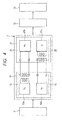
- Fig. 3 is a block diagram showing one example of a circuit block of a transmission reception part of the semiconductor device shown in Fig. 1
- Fig. 4 is a diagram showing one example of a system block using the semiconductor device shown in Fig. 1
- Fig. 5 is a penetration plan view showing one example of an inductor arrangement in each semiconductor chip of the semiconductor device shows in Fig. 1 , Fig.
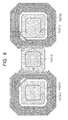
- FIG. 6 is a plan view enlarging and showing one example of the inductor arrangement shown in Fig. 5
- Fig. 7 is a conceptual diagram showing one example of pad heights in two semiconductor chips of the semiconductor device of Fig. 1
- Fig. 8 is a withstand voltage conceptual diagram showing one example of a relationship between a withstand voltage and a distance of sealing resin in the semiconductor device of Fig. 1 .
- the semiconductor device (semiconductor package) shown in Fig. 1 and Fig. 2 is one over which two semiconductor chips are mounted and integrated into a single package.
- a transmission part and a reception part for transmitting and receiving a signal between the both chips are formed, the semiconductor chips are electrically coupled with each other using wires, respectively.
- two inductors (coils) are arranged and the electric signal is transmitted between the inductors without contact between the inductors by bringing the two inductors into inductive coupling in each chip.
- power supply voltages between the inductors that are brought into the inductive coupling are, for example, about several volts on the low voltage side and about several hundred volts to several thousand volts, which are different largely from each other.
- the above-mentioned inductors transmit an electric signal in a non-contact state therebetween through an insulating layer.
- a semiconductor chip (a first semiconductor chip) 11 that has a surface 11a over which multiple pads 11c, 11d, 11e, and 11f are arranged and a semiconductor chip (a second semiconductor chip) 21 that has a surface 21a over which multiple pads 21c, 21d, 21e, and 21f are arranged are incorporated therein.
- the semiconductor chip 11 is mounted over an upper surface (a first upper surface) 14a that a thin-plated die pad (a first chip mounting part) 14 has, and on the other hand the semiconductor chip 21 is mounted over an upper surface (a second upper surface) 24a that a thin-plated die pad (a second chip mounting part) 24 has.
- a back surface 11b of the semiconductor chip 11 is bonded to the die pad 14 with a medium of a die bonding material 2 (an adhesive) interposed therebetween, and a back surface 21b of the semiconductor chip 21 is bonded to the die pad 24 with a medium of the die bonding material 2 interposed therebetween.
- the semiconductor chip 11 includes a transmission part (a first transmission part) 12 for transmitting a signal to the outside and a reception part (a first reception part) 13 for receiving a signal from the outside, and on the other hand the semiconductor chip 21 also includes a transmission part (a second transmission part) 22 for transmitting a signal to the outside and a reception part (a second reception part) 23 for receiving a signal from the outside.
- the SOP1 includes multiple inner leads (first leads) 16 that are arranged adjacent to the die pad 14, multiple inner leads (second leads) 26 that are arranged adjacent to the die pad 24, a suspension lead (a first suspension lead) 15 for supporting the die pad 14, and a suspension lead (a second suspension lead) 25 for supporting the die pad 24.
- the SOP1 includes a wire group (a first wire group) 6 that electrically couples the semiconductor chip 11 and the semiconductor chip 21 and includes multiple wires (first wires) 6a, and a wire group (a second wire group) 7 that electrically couples the semiconductor chip 11 and the semiconductor chip 21 and includes multiple wires (second wires) 7a.
- the SOP1 includes a wire group (a third wire group) 18 that electrically couples the semiconductor chip 11 and the multiple inner leads 16 and includes multiple wires (third wires) 18a, and a wire group (a fourth wire group) 28 that electrically couples the semiconductor chip 11 and the multiple inner leads 26 and includes multiple wires (fourth wires) 28a.
- the SOP1 includes a sealing body 3 that is formed with a resin and seals respective parts of the semiconductor chips 11, 21, the die pads 14, 24, and the suspension leads 15, 25, parts of the multiple first and second leads (the inner leads 16, 26), and the multiple wires 6a, 7a, 18a, and 28a, respectively.
- the sealing body 3 has: a first side 3a extending along a first direction 4; a second side 3b extending along a second direction 5 that is substantially perpendicular to the first direction 4; a third side 3c that faces the first side 3a and extends along the first direction 4; and a fourth side 3d that faces the second side 3b and extends along the second direction 5.
- each of the multiple first leads are arranged along the first side 3a of the sealing body 3, and on the other hand the multiple second leads are arranged along the third side 3c of the sealing body 3.
- each of the multiple first leads is comprised of the inner lead 16 arranged inside the sealing body 3 and the outer lead 17 that links to the inner lead 16 and is arranged outside the sealing body 3 to serve an external terminal of the SOP1.
- each of the multiple outer leads 17 is bent and formed into a shape of a gull wing and is furnished with exterior plating 8 over each surface.
- each of the multiple second leads is comprised of the inner lead 26 arranged inside the sealing body 3 and the outer lead 27 that links to the inner lead 26 and is arranged outside the sealing body 3 to serve an external terminal of the SOP1, and each of the multiple outer leads 27 is bent and formed into the shape of a gull wing and is furnished with the exterior plating 8 over each surface.
- the semiconductor chip 11 and the semiconductor chip 21 are the same semiconductor chip, and as shown in Fig. 1 , the semiconductor chip 21 is mounted over the die pad 24 being rotated to a mounting direction of semiconductor chip 11 by 180 degrees.
- the multiple pads 11c electrically coupled with the transmission part 12 and multiple pads 11d electrically coupled with the reception part 13 are arranged.
- the multiple pads 21c electrically coupled with the transmission part 22 and the multiple pads 21d electrically coupled with the reception part 23 are arranged.
- the multiple pads 11c of the semiconductor chip 11 and the multiple pads 21d of the semiconductor chip 21 are electrically coupled with one another through the wires 6a of the wire group 6, and on the other hand the multiple pads 11d of the semiconductor chip 11 and the multiple pads 21c of the semiconductor chip 21 are electrically coupled with one another through the wires 7a of the wire group 7.
- the transmission part 12 in the semiconductor chip 11 includes a transmission circuit 12a, a coil (a first coil) 12b electrically coupled with the transmission circuit 12a, and a coil (a second coil) 12c that is arranged over the coil 12b, and is insulated (separated) from the coil 12b, further is electrically coupled with some pads 11c among the multiple pads 11c.
- the reception part 13 in the semiconductor chip 11 includes the reception circuit 13a that is coupled with some pads 11d among the multiple pads 11d.
- the transmission part 22 in the semiconductor chip 21 includes a transmission circuit 22a, a coil (a fourth coil) 22c electrically coupled with the transmission circuit 22a, and a coil (a third coil) 22b that is arranged over the coil 22c, is electrically insulated (separated) from the coil 22c, and is coupled with some pads 21c among the multiple pads 21c.
- the reception part 23 in the semiconductor chip 21 includes a reception circuit 23a electrically coupled with some pads 21d among the multiple pads 21d.
- the SOP1 of this embodiment is a two-channel version semiconductor package that has a pair of coils and over which the transmission part and the reception part (the communication parts) are provided, respectively.
- some pads 11c coupled with the coils 12c in the semiconductor chip 11 in plan view are arranged so as to be enclosed by the coils 12c on their peripheries. That is, as shown in an enlarged view of Fig. 6 , the some pads 11c are arranged inside the spirals of the coils 12c. Moreover, the pad 11c for the GND (or the power supply) is arranged between the two coils 12c. Incidentally, in the two coils 12c, winding directions of the spirals are reverse directions.
- the coils 12c are formed over the surface 11a of the semiconductor chip 11 with a medium of an insulating layer 11m interposed therebetween, and are made of copper (Cu) wiring, for example (the insulating layer 11m is made of polyimide, for example).
- the coils 22b formed in the semiconductor chip 21 have also the same arrangement as that of the coils 12c, and are made of the same copper (Cu) wiring as that of the coils 12c.
- the coil 12b of the semiconductor chip 11 and the coil 22c of the semiconductor chip 21 shown in Fig. 3 have the same arrangement.
- a system including the transmission part 12 and the reception part 13 of the semiconductor chip 11 is designated as a first power supply system 9
- a system including the transmission part 22 and the reception part 23 of the semiconductor chip 21 is designated as a second power supply system 10.
- a power supply voltage of the first power supply system 9 is a low voltage (about several volts), and on the other hand a power supply voltage of the second power supply system 10 is a high voltage (about several hundred volts to several thousand volts).
- the inter-wire distance L (L in Fig. 3 ) between the wire 6a and the wire 7a is made larger than any inter-wire distances in the wire group 6 and in the wire group 7.
- the inter-wire distance L (L in Fig. 3 ) of the wires that are closest to each other is made larger than any inter-wire distances in the wire group 6 and in the wire group 7.
- the inter-wire distance L is 0.4 mm or more.
- the withstand voltage can be secured.
- a voltage value differs largely between the first communication part to which the power supply voltage (low voltage) of the first power supply system 9 is supplied and the second communication part to which the power supply voltage (high voltage) of the second power supply system 10 is supplied, by setting (securing) the inter-wire distance between the above-mentioned first communication part and the above-mentioned second communication part wide open, it is possible to secure the withstand voltage. This can prevent electric short circuit between the wire of the above-mentioned first communication part and the wire of the above-mentioned second communication part from occurring, and as a result, improvement of the reliability of the SOP1 can be attained.
- the reliability can be improved while attaining further miniaturization of the SOP1 compared to a configuration using a photocoupler by having adopted inductor coupling.
- a configuration using the inductor since a configuration using the inductor has higher followability to a fast signal than the configuration using the photocoupler, it can support fast signal transmission (transmission of a high-frequency signal).
- the SOP1 of this embodiment is applicable, for example, to automobiles (EV: electric vehicle, HV: hybrid vehicle), motor control systems of electrical household appliances such as a washing machine, a switching regulator, an illumination controller, a solar photovoltaic generation controller, a cellular phone, a mobile communication device, or the like.
- EV electric vehicle
- HV hybrid vehicle
- motor control systems of electrical household appliances such as a washing machine, a switching regulator, an illumination controller, a solar photovoltaic generation controller, a cellular phone, a mobile communication device, or the like.
- the SOP1 can be electrically coupled with loads such as a control circuit 31, a drive circuit 32, and a motor 33.
- the semiconductor chip 11 has the semiconductor chip 11 controlled by the control circuit 31, performs signal transmission by the inductor coupling between the semiconductor chip 11 and the semiconductor chip 21, further, transmits a signal to the drive circuit 32 through the semiconductor chip 21, and makes the drive circuit 32 drive the motor 33, etc.
- the semiconductor chip 11 is a low voltage chip to which the power supply voltage of the first power supply system 9 is supplied and the power supply voltage at that time is about 5 V, for example; on the other hand, the semiconductor chip 21 is a high voltage chip to which the power supply voltage of the second power supply system 10 is supplied, and the power supply voltage at that time is 600 V to 1000 V or a voltage exceeding those voltages, for example.
- a distance (inter-die pad distance) M between the die pad 14 and the die pad 24 is made larger than both a distance N between the die pad 14 and multiple inner leads 16 and a distance P between the die pad 24 and the multiple inner leads 26 (M > N, M > P).
- coupling (ground bonding) with a wire is made between the die pad 14 and the semiconductor chip 11 through multiple wires (fifth wires) 19a, and on the other hand the coupling (the ground bonding) with a wire is also made between the die pad 24 and the semiconductor chip 21 through multiple wires (sixth wires) 29a; therefore, a potential difference arises also between the both die pads.
- the withstand voltage is securable by making large a distance M between the die pad 14 and the die pad 24.
- the semiconductor chip 11 has on its surface 11a: a side (a first chip side) 11g extending in the first direction 4; a side (a second chip side) 11h facing the side 11g and extending in the first direction 4; a side (a third chip side) 11i intersecting the side 11g and extending in the second direction 5; and a side (a fourth chip side) 11j facing the side 11i and extending in the second direction 5.
- the side 11g of the semiconductor chip 11 faces the die pad 24, and on the other hand the side 11 h of the semiconductor chip 11 faces a tip of multiple inner leads 16.
- the multiple pads 11d are arranged so as to be closer to the side 11g of the semiconductor chip 11 than the multiple pads 11c are. That is, the multiple pads 11d are arranged in positions closer to the side 11g than positions of an imaginary line C1 that is formed by the multiple pads 11c in a line. That is, since the coil 12c is arranged in a region peripheral to the pad 11c, the pad 11d is arranged away from the pad 11c.
- the semiconductor chip 21 has also a side 21g (a first chip side) extending in the first direction 4, a side (a second chip side) 21h facing the side 21g and extending in the first direction 4, a side (a third chip side) 21i intersecting the side 21h and extending in the second direction 5, and a side 21j (a fourth chip side) facing the side 21i and extending in the second direction 5.
- the side 21g of the semiconductor chip faces the die pad 14, and on the other hand the side 21h of the semiconductor chip 21 h faces tips of the multiple inner leads 26.
- the multiple pads 21d are arranged so as to be closer to the side 21g of the semiconductor chip 21 than the multiple pads 21c are. That is, the multiple pads 21d are arranged in positions closer to the side 21g than positions of an imaginary line C2 that is formed by the multiple pads 21c in a line. That is, since the semiconductor chip 21 is the same chip as the semiconductor chip 11 and since the coil 22b is arranged on the periphery of the pad 21c, the pad 21d is arranged away from the pad 21c.
- the multiple pads (the fifth pads) 11e are arranged along the side 11i, and some pads 11e among the multiple pads 11e are electrically coupled with the upper surface 14a of the die pad 14 through the wires (the fifth wires) 19a of a wire group 19 (a fifth wire group) 19.
- a long and narrow through hole 14b is provided in a region of the upper surface 14a between the semiconductor chip 11 and a portion where the wire 19a is coupled with the upper surface 14a of the die pad 14.
- the multiple pads (the seventh pads) 21e are arranged along the side 21i over its surface 21a, and some pads 21e among the multiple pads 21e are electrically coupled with the upper surface 24a of the die pad 24 through the wires (the sixth wires) 29a of a wire group (a sixth wire group) 29.
- a long and narrow through hole 24b is provided in a region of the upper surface 24a between the semiconductor chip 21 and a portion where the wire 29a is coupled with the upper surface 24a of the die pad 24.
- the through holes 14b, 24b are formed in the die pads 14, 24, it can be prevented that the wires 19a, 29a cannot be coupled thereto due to outflow of the die bond material (the adhesive) 2. That is, even if the die bonding material 2 flows out, the die bonding material 2 can be accumulated in the through holes 14b, 24b, and it is possible to prevent an outflow of the die bonding material 2 to a region where the wires 19a, 29a are coupled.
- the through holes 14b, 24b may be concave slots as far as they are in a shape capable of accumulating the die bonding material 2 that flowed out, and also in that case, the same effect can be obtained.
- a resin that forms the sealing body 3 can be filled in the through holes 14b, 24b, which can enhance a resin lock effect (an effect of increasing adhesion of the resin and the die pads) of the resin and the die pads 14, 24.
- a resin lock effect an effect of increasing adhesion of the resin and the die pads
- areas of the die pads 14, 24 in plan view that occupies an area of the sealing body 3 in plan view are high as compared with areas of the inner leads 16, 26 in plan view, increasing the resin lock effect is effective in enhancing resistance at the time of reflow.
- the suspension lead 15 of the SOP1 is arranged along the first side 3a of the sealing body 3, the outer leads 17 that are respective parts of the multiple first leads and also a part of the suspension lead 15 are exposed from the first side 3a of the sealing body 3 as external terminals.
- the suspension leads 15 are leads to which the ground voltage can be supplied from the outside, and the pads 11e to each of which the wire is not coupled among the multiple pads 11e are pads to which power supply voltage can be supplied from the outside.
- the suspension lead 25 is arranged along the third side 3c of the sealing body 3, and the outer leads 27 that are parts of the multiple second leads and a part of the suspension lead 25 (the outer lead 27) are exposed from the third side 3c of the sealing body 3 as external terminals.
- the suspension lead 25 is a lead to which the ground voltage can be supplied from the outside, and the pads 21e to each of which the wire is not coupled among the multiple pads 21e are pads to which power supply voltage can be supplied from the outside.
- the semiconductor chip 21 is the same chip as the semiconductor chip 11, even when the semiconductor chip 21 is mounted being rotated to the semiconductor chip 11 by 180 degrees, it is possible to easily supply the ground voltage and the power supply voltage thereto from the outside.
- the multiple pads (the sixth pads) 11f are arranged along the side (the fourth chip side) 11j, some pads 11f of the multiple pads 11f are electrically coupled with some inner leads 16 of the multiple inner leads 16 through some wires 18a in the wire group (the third wire group) 18. Furthermore, leads that are coupled with some pads 11f among the multiple pads 11f are exposed from the first side 3a of the sealing body 3 as the outer leads 17, and are leads to which the power supply voltage can be supplied from the outside. Incidentally, the pads 11f to each of which the wire is not coupled among the multiple pads 11f are pads to which the ground voltage can be supplied from the outside.
- the multiple pads (the eighth pads) 21f are arranged along the side (the fourth chip side) 21j over its surface 21a, and some pads 21f of the multiple pads 21f are electrically coupled with some inner leads 26 of the multiple inner leads 26 through some wires 28a in the wire group (the fourth wire group) 28. Furthermore, leads coupled with the some pads 21f of the multiple pads 21f are exposed from the third side 3c of the sealing body 3 as the outer leads 27, and are leads to which the power supply voltage can be supplied from the outside. Incidentally, the pads 21f to which the wires are not coupled among the multiple pads 21f are pads to which the ground voltage can be supplied from the outside.
- the coils 12c are arranged on the peripheries of the multiple pads 11c over the surface 11a of the semiconductor chip 11, these multiple pads 11c are arranged more inside the semiconductor chip 11 than the multiple pads 11d in plan view. That is, the pads 11c of the transmission part 12 are arranged in positions more inside the semiconductor chip 11 than the pads 11d of the reception part 13.
- the semiconductor chip 11 and the semiconductor chip 21 are the same chip. Therefore, similarly, since the coils 22b are arranged on the peripheries of the multiple pads 21c over the surface 21a of the semiconductor chip 21, the multiple pads are arranged more inside of the semiconductor chip 21 than the multiple pads 21d in plan view. That is, the pads 21c of the transmission part 22 are arranged in positions more inside the semiconductor chip 21 than the pads 21d of the reception part 23.
- an insulating layer 11k provided in the chip and the insulating layer 11m further layered over this insulating layer 11k over its surface 11a are arranged, and these layers secure the withstand voltage between the coils.
- the insulating layer 11m over the surface 11a contains a layer comprised of a polyimide system, a larger withstand voltages can be secured.
- the semiconductor chip 11 and the semiconductor chip 21 are the same chip, also in the coil (the fourth coil) 22c and the coil (the third coil) 22b of the semiconductor chip 21, the insulating layer 11k and the insulating layer 11m (an insulating layer 21m shown in Fig. 5 ) are formed between the both coils like the semiconductor chip 11, and a large withstand voltage is secured.
- a distance Q from wire peaks of the respective wires 6a, 7a of the wire group (the first wire group) 6 and the wire group (the second wire group) 7 to an upper surface 3e of the sealing body 3 be set to be equal to or more than a chip thickness T of the semiconductor chip 11 (semiconductor chip 21) (Q ⁇ T).
- the chip thickness T is 200 ⁇ m to 300 ⁇ m, for example, when considering a package thickness (the miniaturization) of the SOP1, preferably it should be equal to or less than 200 ⁇ m, and it is possible to realize both the miniaturization and securing of the withstand voltage of the SOP1 by setting the above-mentioned distance Q at this time to be equal to or more than 0.2 mm.
- Fig. 8 shows a relationship between the withstand voltage of the sealing resin and the distance (being measured in conformity to ASTM-D149).
- a target withstand voltage is set to be equal to or more than 3.5 kV.
- the distance should be larger than about 0.2 mm, as is clear from Fig. 8 .
- the safety factor was expected to be about 2 times (Min 6.8 kV), and the inter-wire distance L and inter-die pad distance M were set to be equal to or more than 0.4 mm, respectively.
- This calculated value corresponds to the target withstand voltage 3.5 kV or more, exceeding 3.5 kV considerably, and therefore, the distance Q from the wire peak to the sealing body upper surface (resin thickness) is set to be equal to or more than 0.2 mm.
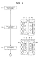
- Fig. 9 is a flowchart and a plan view showing one example of a principal process in an assembly of the semiconductor device
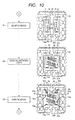
- Fig. 10 is a flowchart and a plan view showing one example of the principal process in the assembly of the semiconductor device of Fig. 1
- Fig. 11 is a flowchart and a plan view showing one example of the principal process in the assembly of the semiconductor device of Fig. 1
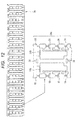
- Fig. 12 is a plan view and enlarged local plan view showing one example of a structure of a lead frame used in the assembly of the semiconductor device of Fig. 1
- Fig. 13 is a sectional view showing one example of a structure of a device region of the lead frame shown in Fig. 12 , Fig.
- Fig. 14 is a sectional view showing one example of a structure after paste coating of the assembly of the semiconductor device of Fig. 1
- Fig. 15 is a sectional view showing one example of a structure after die bonding of the assembly of the semiconductor device of Fig. 1
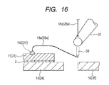
- Fig. 16 is a conceptual diagram showing one example of tools used in wire bonding of the assembly of the semiconductor device of Fig. 1
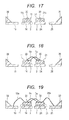
- Fig. 17 is a sectional view showing one example of a structure after bump bonding of the assembly of the semiconductor device of Fig. 1
- Fig. 18 is a sectional view showing one example of a structure after inter-chip bonding of the assembly of the semiconductor device of Fig. 1 , Fig.
- FIG. 19 is a sectional view showing one example of a structure after the wire bonding of the assembly of the semiconductor device of Fig. 1
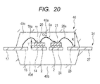
- Fig. 20 is a local sectional view showing one example of a structure after clamping with a mold in an encapsulation process of the assembly of the semiconductor device of Fig. 1 .
- Fig. 21 is a local plan view showing one example of a resin injection direction after clamping with the mold in Fig. 20
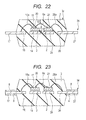
- Fig. 22 is a sectional view showing one example of a structure after encapsulation of the assembly of the semiconductor device of Fig. 1
- Fig. 23 is a sectional view showing one example of a structure after exterior plating formation of the assembly of the semiconductor device of Fig. 1
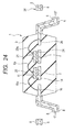
- Fig. 24 is a local sectional view showing one example of a structure after cutting and forming of the assembly of the semiconductor device of Fig. 1 .
- a lead frame 34 is prepared that has the die pad 14 supported by the suspension lead 15, the die pad 24 supported by the suspension lead 25, the multiple inner leads 16 arranged adjacent to the die pad 14, and the multiple inner leads 26 arranged adjacent to the die pad 24.
- many device regions 34a in each of which a single package is formed are formed in a matrix array in the lead frame 34, which is a so-called multiple metallic lead frame (for example, made of a copper alloy, a steel-nickel alloy, etc.) in a thin plate shape.
- the lead frame 34 which is a so-called multiple metallic lead frame (for example, made of a copper alloy, a steel-nickel alloy, etc.) in a thin plate shape.
- Step S2 of Fig. 9 Ag paste application shown in Step S2 of Fig. 9 is performed.
- Ag paste is applied over each of the die pad 14 and the die pad 24 as the die bonding material (the adhesive) 2.
- Step S3 of Fig. 9 is performed.
- the semiconductor chip 11 is mounted over the die pad 14 through the die bonding material 2
- the semiconductor chip 21 is mounted over the die pad 24 through the die bonding material 2.
- the semiconductor chip 11 and the semiconductor chip 21 are the same semiconductor chip, and in a die bonding process, the semiconductor chip 21 is mounted over the die pad 24 after being rotated to the mounting direction of the semiconductor chip 11 by 180 degrees as shown in plan view of Step S3 of Fig. 9 .
- the long and narrow through holes 14b, 24b are formed on sides of respective one ends of the die pad 14 and the die pad 24. Since the through holes 14b, 24b are formed in the die pads 14, 24, even when flowing out (bleeding) of the die bonding material occurs, the die bonding material 2 that flowed out can be accumulated in the through holes 14b, 24b.
- the die bonding material 2 can be accumulated in the through holes 14b, 24b, and it is possible to prevent the outflow of the die bonding material 2 to a region where down bonding is performed.
- the through holes 14b, 24b is just to be in a shape that can stop the die bonding material 2 that flowed out, for example, they may be in a shape of a concave slot, etc., and also in that case, the same effect can be obtained.
- the wire bonding is performed.
- a case of adopting an ultrasonic wire bonding system that applies an ultrasonic wave to each of multiple wires through bonding tools such as an ultrasonic horn 37 and a capillary 38 at the time of the wire bonding, as shown in Fig. 16 will be explained. That is, while a wire is drawn out by the capillary 38 provided near a tip of the ultrasonic horn 37, the wire bonding is performed with an ultrasonic wave applied to the wire by the ultrasonic horn 37 and the capillary 38.
- the wire bonding is performed with respective second ends 14d, 24d of the die pad 14 and the die pad 24 pressed down by a clamper 39.
- the die pads 14, 24 have first ends 14c, 24c and the second ends 14d, 24d that face the first ends 14c, 24c in the first direction 4, respectively, further, the suspension leads 15, 25 are coupled to the first ends 14c, 24c of the die pads 14, 24, respectively, and the second ends 14d, 24d are configured to be open ends 14e, 24e, respectively.
- the die pads are easy to flap at the time of the wire bonding. Therefore, at the time of the wire bonding as shown in Fig. 10 , by pressing the second ends 14d, 24d on the side that are not supported by suspension leads of the die pads 14, 24 with the clamper 39, it is possible to suppress flapping of the respective leads, and as a result, to reduce wire bonding defect caused by flapping of the die pads 14, 24.
- respective open ends 14e, 24e of the second end 14d of the die pad 14 and the second end 24d of the die pad 24 are in a free state where they are not coupled with anything at all including suspension leads. Moreover, a reason why the second ends 14d, 24d of the die pads 14, 24 are in a free state where they are not coupled with anything at all is to secure the withstand voltage.
- a letter T lead 36 is arranged in the vicinity of the second ends 14d, 24d of the die pads 14, 24. If suspension leads are coupled, the withstand voltage cannot be secured between them and the letter T lead 36. Therefore, the second ends 14d, 24d are configured to be open ends (single suspension) 14e, 24e, respectively, without being coupled with suspension leads etc.
- the wire bonding is performed while the second ends 14d, 24d on the sides that are not supported by the suspension leads of the die pads 14, 24 are pressed down by the clamper 39.
- the bump bonding shown in Step S4 of Fig. 10 is performed.
- the multiple pads 11c electrically coupled with the transmission part 12 of Fig. 3 and the multiple pads 11d electrically coupled with the reception part 13 are arranged.
- the multiple pads 21c electrically coupled with the transmission part 22 of Fig. 3 and the multiple pads 21d electrically coupled with the reception part 23 are arranged.
- a first stud bump 20 is formed over one pad 11c among the multiple pads 11c of the semiconductor chip 11.
- a second stud bump 30 is formed over one pad 21c among the multiple pads 21c of the semiconductor chip 21.
- Step S5 of Fig. 10 bonding between chips shown in Step S5 of Fig. 10 is performed. That is, as shown in Fig. 1 , some (pads 11c, 11d) of the multiple pads of the semiconductor chip 11 and some (pads 21c, 21d) of the multiple pads of the semiconductor chip 21 are electrically coupled with one another with the multiple wires 6a, 7a, respectively.
- one end of the wire 6a is coupled onto one pad 21d among the multiple pads 21d of the semiconductor 21 of Fig. 1 , and subsequently the other end of the wire 6a is couple onto the first stud bump 20.
- one end of the wire 7a is coupled onto one pad 11d among the multiple pads 11d of the semiconductor 11, subsequently the other end of the wire 7a is couple onto the second stud bump 30, and the bonding between chips is completed as shown in Fig. 18 .
- this process is one that secures a height at which the second bonding is intended to be performed by having forming the stud bump on a second bonding side, whereby the semiconductor chip can be prevented from being damaged.
- the second side is a pad whose insulating layer under the pad is thicker, and the second bonding is performed to it. That is, since two times of the wire bonding are performed on the second side, i.e., the bump bonding and the second bonding, it is desirable that a pad having a thick insulating layer under the pad be selected as the second side. Therefore, in this embodiment, the pads 11c, 21c formed on the insulating layers 11m, 21m shown in Fig. 5 and Fig. 7 are selected as the second side.
- the insulating layers 11m, 21m are configured to be arranged both under the pad over which the first stud bump 20 is formed among the multiple pads 11c of the semiconductor chip 11 and under the pad over which the second stud bump 30 is formed among the multiple pads 21c of the semiconductor chip 21.
- the insulating layers 11m, 21m each contain a layer comprised of a polyimide.
- the multiple pads 11c of the semiconductor chip 11 and the multiple pads 21d of the semiconductor chip 21 are coupled with one another with multiple wires 6a included in the wire group 6, respectively. Furthermore, the multiple pads 11d of the semiconductor chip 11 and the multiple pads 21c of the semiconductor chip 21 are coupled with one another with the multiple wires 7a included in the wire group 7, respectively.
- the wire bonding is performed so that the inter-wire distance L between the wire 6a that is closest to the wire group 7 in the wire group 6 and the wire 7a that is closest to the wire group 6 in the wire group 7 may become larger than any inter-wire distances in the wire group 6 and in the wire group 7.
- the inter-wire distance L is 0.4 mm or more.
- the assembly of the SOP1 of this embodiment by making the inter-wire distance L between the wire 6a that is closest to the wire group 7 in the wire group 6 and the wire 7a that is closest to the wire group 6 in the wire group 7 larger than any inter-wire distances in the wire group 6 and in the wire group 7, it is possible to secure the withstand voltage of the SOP1.
- the semiconductor chip 11 and the semiconductor chip 21 in the case where voltage values differ largely between the first communication part to which the power supply voltage (low voltage) of the first power supply system 9 of Fig. 3 is supplied and the second communication part to which the power supply voltage (high voltage) of the second power supply system 10 is supplied, it is possible to secure the withstand voltage by making the inter-wire distance in the above-mentioned first communication part and the above-mentioned second communication part wide open. This can prevent the electric short circuit between the wire of the above-mentioned first communication part and the wire of the above-mentioned second communication part from occurring, and as a result, the improvement of the reliability of the SOP1 can be attained.
- Step S6 of Fig. 10 is performed.
- the wire bonding between the chip and the lead is performed. That is, as shown in Fig. 1 and Fig. 19 , some (the pad 11f) of the multiple pads of the semiconductor chip 11 and the multiple inner leads 16 are electrically coupled with one another with multiple wires 18a, respectively. Moreover, some (pad 21f) of the multiple pads of the semiconductor chip 21 and the multiple inner leads 26 are electrically coupled with one another with the multiple wires 28a, respectively.
- some (the pad 11e) of the multiple pads of the semiconductor chip 11 and the suspension lead 15 are electrically coupled with the wire 19a
- some (the pad 21e) of the multiple pads of the semiconductor chip 21 and the suspension lead 25 are electrically coupled with the wire 29a.
- the ground bonding is performed to the die pads 14, 24 from the semiconductor chip 11 and the semiconductor chip 21, respectively.
- the ground bonding is performed so as to make coupling to the sides of the first ends 14c, 24c (sides that are not pressed down by the clamper 39) that are opposite sides to the second ends 14d, 24d.
- the ground bonding can be performed with the die pads 14, 24 firmly pressed down on the sides of the second ends 14d, 24d of the open ends 14e, 24e.
- the wire bonding is performed so that the wire may jump over the through holes 14b, 24b provided in the die pads 14, 24. Since the sides of the first ends 14c, 24c of the die pads 14, 24 have comparatively large areas, exfoliation takes place easily between the die pads 14, 24 and the resin. Then, since the through holes 14b, 24b are formed in the areas of the die pads 14, 24 with large areas, adhesion of the die pads 14, 24 and the resin in this areas can be improved, so that exfoliation between the die pads 14, 24 and the resin at the time of reflow can be reduced.
- the wire bonding process is ended by the above.
- the encapsulation (sealing) shown in Step S7 of Fig. 11 is performed after completion of the wire bonding.
- the semiconductor chips 11, 21, respective parts of the suspension leads 15, 25, the die pads 14, 24, some of the multiple first and second leads (the inner leads 16, 26), and the multiple wires 6a, 7a, 18a, 28a, 19a, and 29a are sealed by sealing resin 41 (insulating resin) shown in Fig. 21 . That is, using the sealing resin 41, the sealing body 3 is formed that has the first side 3a and the third side 3c that extend in the first direction 4 shown in Fig. 1 and the second side 3b and the fourth side 3d that extend in the second direction 5 substantially perpendicular to the first direction 4.
- the sealing resin 41 of Fig. 21 is poured toward the fourth side 3d from the second side 3b of the sealing body 3 shown in Fig. 1 to form the sealing body 3.
- the suspension leads 15, 25 are provided so as to be closer to the second side 3b than the fourth side 3d of the sealing body 3 are in plan view, and as shown in Fig. 21 , by arranging a gate 40e for molding on the suspension lead side and injecting the sealing resin 41 from the suspension lead side, it is possible to suppress the flapping of the die pads 14, 24 at the time of resin injection.
- the sealing resin 41 comes out from a side opposite to the gate 40e, and flows into the next cavity.
- a resin forming mold 40 of Fig. 20 used in this embodiment includes a pair of an upper mold (a first mold) 40a and a lower mold (a second mold) 40b; a cavity (a first cavity) 40c is formed in the upper mold 40a, and on the other hand a cavity (a second cavity) 40d is formed in the lower mold 40b.
- a depth R of the cavity 40c of the upper mold 40a is a depth capable of forming a relationship so that the distance Q from the wire peak of the wire 6a (the wire 7a) of the wire group 6 (the wire group 7) to the upper surface 3e of the sealing body 3 may become equal to or more than the chip thickness T of the semiconductor chip 11 (Q ⁇ T).
- the resin forming mold 40 that includes the upper mold 40a having the cavity 40c as shown in Fig. 20 and a lower mold 40b making a pair with the upper mold 40a and facing the upper mold 40a is prepared.
- the lead frame 34 is positioned so that the semiconductor chips 11, 21 may be located within the cavity 40c of the upper mold 40a. Furthermore, after holding the lead frame 34 with the upper mold 40a and the lower mold 40b, the sealing resin 41 is poured into the cavity 40c from the gate 40e linking to the cavity 40c.
- the sealing resin 41 is injected (supplied) into the cavity 40c from the gate 40e that is arranged on the suspension lead side.
- the sealing body 3 can be formed so that the distance Q from the wire peak to the sealing body upper surface may become equal to or more than the chip thickness T of the semiconductor chip 11 (Q ⁇ T).
- the sealing resin 41 can be embedded into each of the through holes 14b, 24b at the time of the resin injection, and the resin lock effect of the resin 41 for sealing (the sealing body 3) and the die pads 14, 24 can be enhanced.
- the SOP1 since the areas of the die pads 14, 24 in plan view are large as compared with the area of the sealing body 3 in plan view, it is very effective to enhance the resin lock effect.
- Step S8 of Fig. 11 exterior plating shown in Step S8 of Fig. 11 is performed. That is, as shown in Fig. 23 , the exterior plating 8 comprised of solder, etc. is performed over respective surfaces of the multiple outer leads 17, 27 exposed from side faces of the sealing body 3.
- Step S9 of Fig. 11 After that, cutting and forming shown in Step S9 of Fig. 11 are performed. That is, the outer leads 17, 27 that link to respective leads 15, 25 shown in Fig. 1 and the outer leads 17, 27 that link to respective multiple leads 16, 26 shown in Fig. 24 are cut off from the lead frame 34, and each of the multiple outer leads 17, 27 is formed and bent into the shape of a gull wing.
- the letter T leads 35, 36 are provided being linking to the lead frame 34, and at a stage where the sealing body 3 is formed, the letter T leads 35, 36 are in a state where their tips are embedded in the inside of the sealing body 3.
- the package body (the SOP body) is in a state of being supported by the lead frame 34 with the letter T leads 35, 36, and does not come off from the lead frame 34.
- Fig. 25 is a plan view showing a structure of a semiconductor device of a modification of the embodiment with the sealing body penetrated.
- Fig. 25 shows a 16-pin SOP42 of a four-channel version as a modification of the above-mentioned semiconductor device. That is, even if the number of channels increases to four channels, it is possible to secure the withstand voltage, like the SOP1 of the above-mentioned embodiment, by making larger the inter-wire distance L between the wire 6a that is closest to the wire group 7 in the wire group 6 that performs coupling between the transmission part and the reception part (communication parts) and the wire 7a that is closest to the wire group 6 in the wire group 7 than any inter-wire distances in the wire group 6 and in the wire group 7.
- the semiconductor chip 11 and the semiconductor chip 21 are not necessarily required to be the same chip.
- the semiconductor device is a semiconductor device such that the semiconductor chips have communication functions, respectively, and perform communication therebetween through wires and also by the inductor coupling, and the voltage values are different between the communication parts, the multiple semiconductor chips that are mounted thereon are not required to be the same chip.
Landscapes
- Engineering & Computer Science (AREA)
- Power Engineering (AREA)
- Computer Networks & Wireless Communication (AREA)
- Signal Processing (AREA)
- Wire Bonding (AREA)
- Semiconductor Integrated Circuits (AREA)
- Lead Frames For Integrated Circuits (AREA)
Applications Claiming Priority (1)
| Application Number | Priority Date | Filing Date | Title |
|---|---|---|---|
| JP2013133174A JP6129659B2 (ja) | 2013-06-25 | 2013-06-25 | 半導体装置およびその製造方法 |
Publications (2)
| Publication Number | Publication Date |
|---|---|
| EP2822031A2 true EP2822031A2 (fr) | 2015-01-07 |
| EP2822031A3 EP2822031A3 (fr) | 2015-06-10 |
Family
ID=50842161
Family Applications (1)
| Application Number | Title | Priority Date | Filing Date |
|---|---|---|---|
| EP14170909.7A Ceased EP2822031A3 (fr) | 2013-06-25 | 2014-06-03 | Dispositif semi-conducteur et son procédé de fabrication |
Country Status (6)
| Country | Link |
|---|---|
| US (2) | US9754865B2 (fr) |
| EP (1) | EP2822031A3 (fr) |
| JP (1) | JP6129659B2 (fr) |
| KR (1) | KR20150000831A (fr) |
| CN (1) | CN104253102B (fr) |
| HK (1) | HK1205357A1 (fr) |
Families Citing this family (35)
| Publication number | Priority date | Publication date | Assignee | Title |
|---|---|---|---|---|
| JP2014220439A (ja) | 2013-05-10 | 2014-11-20 | ルネサスエレクトロニクス株式会社 | 半導体装置の製造方法および半導体装置 |
| JP6522402B2 (ja) * | 2015-04-16 | 2019-05-29 | ローム株式会社 | 半導体装置 |
| US10304806B2 (en) | 2015-07-16 | 2019-05-28 | Pezy Computing K.K. | Semiconductor device |
| JP6503264B2 (ja) * | 2015-08-27 | 2019-04-17 | ルネサスエレクトロニクス株式会社 | 半導体装置 |
| JP2017098334A (ja) * | 2015-11-19 | 2017-06-01 | ルネサスエレクトロニクス株式会社 | 半導体装置 |
| JP2017112327A (ja) * | 2015-12-18 | 2017-06-22 | ルネサスエレクトロニクス株式会社 | 半導体装置 |
| CN105575941B (zh) * | 2016-02-03 | 2018-01-02 | 中芯集成电路(宁波)有限公司 | 一种双芯片封装实现的大功率谐振电源控制芯片 |
| US10833595B2 (en) * | 2016-07-01 | 2020-11-10 | Rohm Co., Ltd. | Semiconductor device with upper and lower switching devices and isolation transformer |
| JP2018041956A (ja) * | 2016-09-06 | 2018-03-15 | エイブリック株式会社 | 半導体装置の製造方法 |
| CN107799498A (zh) * | 2016-09-06 | 2018-03-13 | 精工半导体有限公司 | 半导体装置的制造方法 |
| JP6768569B2 (ja) * | 2017-03-21 | 2020-10-14 | ルネサスエレクトロニクス株式会社 | 半導体装置の製造方法および半導体装置 |
| JP6909995B2 (ja) * | 2017-06-27 | 2021-07-28 | パナソニックIpマネジメント株式会社 | アイソレータ |
| US10734331B2 (en) * | 2017-08-16 | 2020-08-04 | Texas Instruments Incorporated | Integrated circuit with an embedded inductor or transformer |
| US10312185B2 (en) * | 2017-10-05 | 2019-06-04 | Texas Instrument Incorporated | Inductively coupled microelectromechanical system resonator |
| DE112018004478B4 (de) | 2017-10-13 | 2025-03-27 | Rohm Co., Ltd. | Elektronikkomponente |
| CN109872869B (zh) * | 2017-12-04 | 2021-12-28 | 万国半导体(开曼)股份有限公司 | 一种隔离耦合结构 |
| CN108133926B (zh) * | 2017-12-14 | 2024-05-24 | 常州星海电子股份有限公司 | 一种整流桥 |
| CN110010509B (zh) * | 2018-01-05 | 2023-10-20 | 光宝新加坡有限公司 | 双引线架磁耦合封装结构及其制造方法 |
| JP2020017692A (ja) * | 2018-07-27 | 2020-01-30 | Tdk株式会社 | 電子部品パッケージ |
| KR102564605B1 (ko) * | 2018-12-21 | 2023-08-14 | 에스케이하이닉스 주식회사 | 반도체 장치 및 반도체 장치의 제조 방법 |
| JP6718540B2 (ja) * | 2019-04-24 | 2020-07-08 | ローム株式会社 | 半導体装置 |
| US11538740B2 (en) * | 2019-07-15 | 2022-12-27 | Texas Instruments Incorporated | Leads for semiconductor package |
| US20210043466A1 (en) * | 2019-08-06 | 2021-02-11 | Texas Instruments Incorporated | Universal semiconductor package molds |
| JP7035117B2 (ja) * | 2020-06-12 | 2022-03-14 | ローム株式会社 | 半導体装置 |
| JP7541456B2 (ja) * | 2020-09-10 | 2024-08-28 | ローム株式会社 | 半導体装置 |
| JP7527906B2 (ja) * | 2020-09-10 | 2024-08-05 | ローム株式会社 | 半導体装置 |
| JP7603400B2 (ja) | 2020-09-10 | 2024-12-20 | ローム株式会社 | 半導体装置 |
| JP7541455B2 (ja) * | 2020-09-10 | 2024-08-28 | ローム株式会社 | 半導体装置 |
| JPWO2022176690A1 (fr) * | 2021-02-16 | 2022-08-25 | ||
| JP7685924B2 (ja) * | 2021-10-08 | 2025-05-30 | ルネサスエレクトロニクス株式会社 | 半導体装置およびその製造方法 |
| US20240038439A1 (en) * | 2022-07-28 | 2024-02-01 | Qualcomm Incorporated | Inductor packages employing wire bonds over a lead frame to form integrated inductor(s), and related integrated circuit (ic) packages and fabrication methods |
| JP2024083816A (ja) * | 2022-12-12 | 2024-06-24 | キオクシア株式会社 | 半導体装置及び半導体装置の製造方法 |
| CN116072663B (zh) * | 2023-02-28 | 2024-02-02 | 海信家电集团股份有限公司 | 功率模块及具有其的电子设备 |
| JPWO2024195480A1 (fr) * | 2023-03-22 | 2024-09-26 | ||
| DE112024001400T5 (de) * | 2023-03-24 | 2026-01-15 | Rohm Co., Ltd. | Halbleiterbauteil |
Citations (3)
| Publication number | Priority date | Publication date | Assignee | Title |
|---|---|---|---|---|
| JPH04223364A (ja) * | 1990-12-25 | 1992-08-13 | Mitsubishi Electric Corp | 半導体装置 |
| JP2009302418A (ja) | 2008-06-17 | 2009-12-24 | Nec Electronics Corp | 回路装置及びその製造方法 |
| US20100052826A1 (en) * | 2004-06-03 | 2010-03-04 | Silicon Laboratories Inc. | Isolator with complementary configurable memory |
Family Cites Families (13)
| Publication number | Priority date | Publication date | Assignee | Title |
|---|---|---|---|---|
| JPH04199559A (ja) * | 1990-11-28 | 1992-07-20 | Mitsubishi Electric Corp | 半導体装置 |
| JPH04258157A (ja) * | 1991-02-12 | 1992-09-14 | Mitsubishi Electric Corp | リ−ドフレ−ム |
| JP4489485B2 (ja) * | 2004-03-31 | 2010-06-23 | 株式会社ルネサステクノロジ | 半導体装置 |
| US7737871B2 (en) * | 2004-06-03 | 2010-06-15 | Silicon Laboratories Inc. | MCU with integrated voltage isolator to provide a galvanic isolation between input and output |
| JP4426955B2 (ja) * | 2004-11-30 | 2010-03-03 | 株式会社ルネサステクノロジ | 半導体装置 |
| JP4551255B2 (ja) * | 2005-03-31 | 2010-09-22 | ルネサスエレクトロニクス株式会社 | 半導体装置 |
| JP2007250891A (ja) * | 2006-03-16 | 2007-09-27 | Fuji Electric Device Technology Co Ltd | パワーエレクトロニクス機器 |
| JP5238562B2 (ja) * | 2009-03-13 | 2013-07-17 | ルネサスエレクトロニクス株式会社 | 半導体装置 |
| JP5390246B2 (ja) * | 2009-04-20 | 2014-01-15 | ルネサスエレクトロニクス株式会社 | 半導体装置 |
| US8283212B2 (en) * | 2010-12-28 | 2012-10-09 | Alpha & Omega Semiconductor, Inc. | Method of making a copper wire bond package |
| JP5514134B2 (ja) | 2011-02-14 | 2014-06-04 | ルネサスエレクトロニクス株式会社 | 半導体装置の製造方法 |
| JP5618873B2 (ja) * | 2011-03-15 | 2014-11-05 | ルネサスエレクトロニクス株式会社 | 半導体装置の製造方法 |
| JP5823798B2 (ja) * | 2011-09-29 | 2015-11-25 | ルネサスエレクトロニクス株式会社 | 半導体装置 |
-
2013
- 2013-06-25 JP JP2013133174A patent/JP6129659B2/ja active Active
-
2014
- 2014-06-03 EP EP14170909.7A patent/EP2822031A3/fr not_active Ceased
- 2014-06-15 US US14/304,949 patent/US9754865B2/en active Active
- 2014-06-20 KR KR20140075826A patent/KR20150000831A/ko not_active Withdrawn
- 2014-06-24 CN CN201410286956.2A patent/CN104253102B/zh active Active
-
2015
- 2015-06-23 HK HK15105948.5A patent/HK1205357A1/xx unknown
-
2017
- 2017-07-27 US US15/662,058 patent/US20170323848A1/en not_active Abandoned
Patent Citations (3)
| Publication number | Priority date | Publication date | Assignee | Title |
|---|---|---|---|---|
| JPH04223364A (ja) * | 1990-12-25 | 1992-08-13 | Mitsubishi Electric Corp | 半導体装置 |
| US20100052826A1 (en) * | 2004-06-03 | 2010-03-04 | Silicon Laboratories Inc. | Isolator with complementary configurable memory |
| JP2009302418A (ja) | 2008-06-17 | 2009-12-24 | Nec Electronics Corp | 回路装置及びその製造方法 |
Also Published As
| Publication number | Publication date |
|---|---|
| JP6129659B2 (ja) | 2017-05-17 |
| US20170323848A1 (en) | 2017-11-09 |
| HK1205357A1 (en) | 2015-12-11 |
| EP2822031A3 (fr) | 2015-06-10 |
| CN104253102B (zh) | 2018-12-28 |
| US9754865B2 (en) | 2017-09-05 |
| JP2015008229A (ja) | 2015-01-15 |
| KR20150000831A (ko) | 2015-01-05 |
| CN104253102A (zh) | 2014-12-31 |
| US20140374890A1 (en) | 2014-12-25 |
Similar Documents
| Publication | Publication Date | Title |
|---|---|---|
| US9754865B2 (en) | Semiconductor device and method for manufacturing the same | |
| US10109565B2 (en) | Semiconductor device | |
| US7981788B2 (en) | Semiconductor device and a manufacturing method of the same | |
| US7923851B2 (en) | Microelectronic assembly with impedance controlled wirebond and conductive reference element | |
| EP2802064B1 (fr) | Module d'alimentation et son procédé d'encapsulation | |
| CN1231765A (zh) | 特别用于置入芯片卡体的芯片模块 | |
| CN103579153A (zh) | 芯片卡模块 | |
| CN100413043C (zh) | 半导体器件的制造方法 | |
| US20110210432A1 (en) | Semiconductor device and method of manufacturing the same | |
| CN103022014A (zh) | 具有天线的封装模块构造及其制造方法 | |
| JP2009094189A (ja) | コネクタ付き半導体パッケージ | |
| JP2017045878A (ja) | 半導体装置 | |
| JPH01132142A (ja) | 半導体装置のパツケージ構造 | |
| EP2846355A1 (fr) | Substrat électrique et procédé de fabrication de celui-ci | |
| JP2008177424A (ja) | 半導体装置 | |
| JP5048627B2 (ja) | リードフレーム及び半導体装置 | |
| KR102617704B1 (ko) | 파워 모듈 및 그의 패키징 방법 | |
| CN116314121A (zh) | 功率模块及其制造方法 | |
| KR200211272Y1 (ko) | 칩 사이즈 패키지 | |
| KR101491258B1 (ko) | 리드 프레임의 제조방법 | |
| KR20230044528A (ko) | 적어도 하나의 안테나를 포함하는 카드용 전자 모듈 및 그 제조 방법 | |
| WO2014182239A1 (fr) | Modules de cartes à puce ultra-minces ayant des bosses de connexion disposées dans des vias d'un substrat et procédés de fabrications de ceux-ci | |
| JP2010102544A (ja) | Icモジュールの製造方法、icカードの製造方法、icモジュール、及びicカード | |
| JP2009218690A (ja) | 信号伝送装置および信号伝送装置の製造方法 |
Legal Events
| Date | Code | Title | Description |
|---|---|---|---|
| PUAI | Public reference made under article 153(3) epc to a published international application that has entered the european phase |
Free format text: ORIGINAL CODE: 0009012 |
|
| 17P | Request for examination filed |
Effective date: 20140603 |
|
| AK | Designated contracting states |
Kind code of ref document: A2 Designated state(s): AL AT BE BG CH CY CZ DE DK EE ES FI FR GB GR HR HU IE IS IT LI LT LU LV MC MK MT NL NO PL PT RO RS SE SI SK SM TR |
|
| AX | Request for extension of the european patent |
Extension state: BA ME |
|
| PUAL | Search report despatched |
Free format text: ORIGINAL CODE: 0009013 |
|
| AK | Designated contracting states |
Kind code of ref document: A3 Designated state(s): AL AT BE BG CH CY CZ DE DK EE ES FI FR GB GR HR HU IE IS IT LI LT LU LV MC MK MT NL NO PL PT RO RS SE SI SK SM TR |
|
| AX | Request for extension of the european patent |
Extension state: BA ME |
|
| RIC1 | Information provided on ipc code assigned before grant |
Ipc: H01L 23/49 20060101AFI20150506BHEP Ipc: H04L 25/02 20060101ALI20150506BHEP Ipc: H01L 23/495 20060101ALN20150506BHEP Ipc: H01F 19/04 20060101ALI20150506BHEP |
|
| RAP1 | Party data changed (applicant data changed or rights of an application transferred) |
Owner name: RENESAS ELECTRONICS CORPORATION |
|
| R17P | Request for examination filed (corrected) |
Effective date: 20151204 |
|
| RBV | Designated contracting states (corrected) |
Designated state(s): AL AT BE BG CH CY CZ DE DK EE ES FI FR GB GR HR HU IE IS IT LI LT LU LV MC MK MT NL NO PL PT RO RS SE SI SK SM TR |
|
| STAA | Information on the status of an ep patent application or granted ep patent |
Free format text: STATUS: EXAMINATION IS IN PROGRESS |
|
| 17Q | First examination report despatched |
Effective date: 20190624 |
|
| STAA | Information on the status of an ep patent application or granted ep patent |
Free format text: STATUS: THE APPLICATION HAS BEEN REFUSED |
|
| 18R | Application refused |
Effective date: 20240914 |