EP2927954B1 - Système de fixation pour un module de puissance - Google Patents
Système de fixation pour un module de puissance Download PDFInfo
- Publication number
- EP2927954B1 EP2927954B1 EP14163131.7A EP14163131A EP2927954B1 EP 2927954 B1 EP2927954 B1 EP 2927954B1 EP 14163131 A EP14163131 A EP 14163131A EP 2927954 B1 EP2927954 B1 EP 2927954B1
- Authority
- EP
- European Patent Office
- Prior art keywords
- power module
- contact
- pressure element
- contact pressure
- molded body
- Prior art date
- Legal status (The legal status is an assumption and is not a legal conclusion. Google has not performed a legal analysis and makes no representation as to the accuracy of the status listed.)
- Active
Links
Images


Classifications
-
- H—ELECTRICITY
- H05—ELECTRIC TECHNIQUES NOT OTHERWISE PROVIDED FOR
- H05K—PRINTED CIRCUITS; CASINGS OR CONSTRUCTIONAL DETAILS OF ELECTRIC APPARATUS; MANUFACTURE OF ASSEMBLAGES OF ELECTRICAL COMPONENTS
- H05K7/00—Constructional details common to different types of electric apparatus
- H05K7/02—Arrangements of circuit components or wiring on supporting structure
-
- H—ELECTRICITY
- H10—SEMICONDUCTOR DEVICES; ELECTRIC SOLID-STATE DEVICES NOT OTHERWISE PROVIDED FOR
- H10W—GENERIC PACKAGES, INTERCONNECTIONS, CONNECTORS OR OTHER CONSTRUCTIONAL DETAILS OF DEVICES COVERED BY CLASS H10
- H10W40/00—Arrangements for thermal protection or thermal control
- H10W40/60—Securing means for detachable heating or cooling arrangements, e.g. clamps
- H10W40/611—Bolts or screws
-
- H—ELECTRICITY
- H10—SEMICONDUCTOR DEVICES; ELECTRIC SOLID-STATE DEVICES NOT OTHERWISE PROVIDED FOR
- H10W—GENERIC PACKAGES, INTERCONNECTIONS, CONNECTORS OR OTHER CONSTRUCTIONAL DETAILS OF DEVICES COVERED BY CLASS H10
- H10W74/00—Encapsulations, e.g. protective coatings
- H10W74/10—Encapsulations, e.g. protective coatings characterised by their shape or disposition
- H10W74/111—Encapsulations, e.g. protective coatings characterised by their shape or disposition the semiconductor body being completely enclosed
- H10W74/114—Encapsulations, e.g. protective coatings characterised by their shape or disposition the semiconductor body being completely enclosed by a substrate and the encapsulations
-
- H—ELECTRICITY
- H10—SEMICONDUCTOR DEVICES; ELECTRIC SOLID-STATE DEVICES NOT OTHERWISE PROVIDED FOR
- H10W—GENERIC PACKAGES, INTERCONNECTIONS, CONNECTORS OR OTHER CONSTRUCTIONAL DETAILS OF DEVICES COVERED BY CLASS H10
- H10W90/00—Package configurations
-
- H—ELECTRICITY
- H10—SEMICONDUCTOR DEVICES; ELECTRIC SOLID-STATE DEVICES NOT OTHERWISE PROVIDED FOR
- H10W—GENERIC PACKAGES, INTERCONNECTIONS, CONNECTORS OR OTHER CONSTRUCTIONAL DETAILS OF DEVICES COVERED BY CLASS H10
- H10W40/00—Arrangements for thermal protection or thermal control
- H10W40/20—Arrangements for cooling
- H10W40/231—Arrangements for cooling characterised by their places of attachment or cooling paths
- H10W40/233—Arrangements for cooling characterised by their places of attachment or cooling paths attached to chips
-
- H—ELECTRICITY
- H10—SEMICONDUCTOR DEVICES; ELECTRIC SOLID-STATE DEVICES NOT OTHERWISE PROVIDED FOR
- H10W—GENERIC PACKAGES, INTERCONNECTIONS, CONNECTORS OR OTHER CONSTRUCTIONAL DETAILS OF DEVICES COVERED BY CLASS H10
- H10W40/00—Arrangements for thermal protection or thermal control
- H10W40/20—Arrangements for cooling
- H10W40/231—Arrangements for cooling characterised by their places of attachment or cooling paths
- H10W40/235—Arrangements for cooling characterised by their places of attachment or cooling paths attached to package parts
-
- H—ELECTRICITY
- H10—SEMICONDUCTOR DEVICES; ELECTRIC SOLID-STATE DEVICES NOT OTHERWISE PROVIDED FOR
- H10W—GENERIC PACKAGES, INTERCONNECTIONS, CONNECTORS OR OTHER CONSTRUCTIONAL DETAILS OF DEVICES COVERED BY CLASS H10
- H10W40/00—Arrangements for thermal protection or thermal control
- H10W40/60—Securing means for detachable heating or cooling arrangements, e.g. clamps
-
- H—ELECTRICITY
- H10—SEMICONDUCTOR DEVICES; ELECTRIC SOLID-STATE DEVICES NOT OTHERWISE PROVIDED FOR
- H10W—GENERIC PACKAGES, INTERCONNECTIONS, CONNECTORS OR OTHER CONSTRUCTIONAL DETAILS OF DEVICES COVERED BY CLASS H10
- H10W74/00—Encapsulations, e.g. protective coatings
- H10W74/10—Encapsulations, e.g. protective coatings characterised by their shape or disposition
-
- H—ELECTRICITY
- H10—SEMICONDUCTOR DEVICES; ELECTRIC SOLID-STATE DEVICES NOT OTHERWISE PROVIDED FOR
- H10W—GENERIC PACKAGES, INTERCONNECTIONS, CONNECTORS OR OTHER CONSTRUCTIONAL DETAILS OF DEVICES COVERED BY CLASS H10
- H10W90/00—Package configurations
- H10W90/701—Package configurations characterised by the relative positions of pads or connectors relative to package parts
- H10W90/751—Package configurations characterised by the relative positions of pads or connectors relative to package parts of bond wires
- H10W90/756—Package configurations characterised by the relative positions of pads or connectors relative to package parts of bond wires between a chip and a stacked lead frame, conducting package substrate or heat sink
Definitions
- the invention relates to a pressing element for a power module according to the preamble of claim 1. Furthermore, the invention relates to such a fastening system according to the preamble of claim 5.
- a power module is a special type of integrated circuit (IC) in which appropriately large housings, transistors and diodes are used to control large currents and voltages. It typically consists of a molded body with an essentially flat surface for bearing against a support structure and a plurality of contact pins protruding from the molded body. Due to the often high heat generation, such power modules are typically installed in such a way that the heat is transferred to the support structure and / or to a heat sink via a contact surface that is metallized over the entire surface, for example, and the connections of the power substrate and, depending on the design and location, possibly via a thermally conductive intermediate layer. With foils or thermally conductive pastes, the smallest unevenness between the power module and the support structure or heat sink can be compensated or the thermal resistance can be reduced.
- IC integrated circuit
- the semiconductor chips in power modules are wired with bonding wires.
- the semiconductor chips and bonding wires are molded with a soft silicone compound.
- Technically more advanced power modules designed as mold modules are hard-potted like conventional ICs. Due to the manufacturing process, the back of the mold module is now not perfectly flat, but is slightly curved from the center outwards. This curvature can no longer be compensated for by foils, pastes or the like, so that the power modules are often pressed against the support structure or the heat sink by pressing elements.
- These pressing elements are typically rigid, mostly elongated plates, with the aim of distributing the pressure and avoiding local Pressure peaks foam mats have to be inserted between the pressure element and the power module, which considerably increases the cost of the components as well as the production.
- the FR2931523A1 a clamp for pressing electronic components on, which has a fastening section which is located next to the components to be fastened, in particular between two. Tabs emanating from this lateral fastening area act on the central areas of the components in order to press them against the base or its seat.
- the EP0785575A2 discloses such a fastening element, the fastening section of which lies on one side next to the electronic component and, in the fastened position, lies directly on the support structure. Only one elongated tab is sufficient to reach a central area of the component and exerts a pressing force solely on its central area.
- the US2009 / 0168358A1 a pressing element with a tab protruding over the component to be fastened. The end piece of this bracket is provided with a plate spring, which again acts centrally on the electronic component.
- EP1536467 discloses a holder and thermal conductor for an electronic component.
- JP2011035265A a variant for a pressing element is disclosed, the fastening element of which is passed through the electronic component to be fastened.
- the pressure element in the form of a circular disc spring does not cover the majority of the edge areas due to the design.
- the US2010012739A1 finally, discloses a fastening element in the form of a tape spanning the electronic component with fastening sections bent towards the support structure. These sections lying on both sides of the component lie directly on the supporting structure in the attached state. The exact position of the introduction of force into the component and thus its contact pressure on the base is not defined.
- the object of the present invention is therefore to provide a pressing element for one or more power modules which, while avoiding the above-mentioned disadvantages, ensures secure, simple fastening that is optimized in terms of heat transfer from the power module to the support structure.
- Another object of the invention is a fastening system using this optimized pressing element.
- the first object is achieved by the features of independent claim 1.
- the further object is achieved by the features of independent claim 5.
- Advantageous further developments are presented in the figures and in the dependent claims.
- the outer sections of the pressure element for a power module extend in the form of a tongue or tab, preferably from a central area of the pressure element, the outer edge areas of which act elastically on edge areas of the power module when the power module and pressure element are in the attached position. A contact force is applied to the power module by means of these edge areas.
- the power module is only subjected to the hold-down or pressing force at the sections that are most curved out of the ideal plane of the housing, namely the corner areas. In the remaining areas, the module remains free and is not touched by the pressure element, so that no protective spacers, mats or the like have to be provided.
- the pressing element also offers a sufficient pretensioning force on the housing of the module, so that from this point of view, too, mats for pressure compensation - as with rigid plates as pressing elements - are not required.
- the housing of the power or molding module between its support structure and the pressure element is brought into a flat shape in which it rests evenly over the entire surface on the support structure. On the one hand it is secured against undesired movements and on the other hand there is heat transfer to the supporting structure and / or a heat sink ensured over the maximum available area.
- a pressure element according to the invention is characterized in that the sections formed on the pressure element are designed as edge strips extending along an edge region of the power module. These edge strips are preferably located on two opposite sides of the pressing element in order to achieve a uniformly distributed introduction of force into the molded body of the power module.
- the sections of the pressing element are preferably located in an edge region with contact pins. As a result, these contact pins are held securely, immovably and in a precisely defined position.
- fastening sections are designed as tabs projecting beyond the power module with bores for receiving connecting elements, preferably in the form of screws, on the pressing element.
- This type of fastening is easy to manufacture, assemble and dismantle, for example when it is necessary to replace the power module.
- At least the edge regions of a further embodiment of the pressing element according to the invention that come into contact with the power module are curved towards the power module. As a result, the achievable contact pressure can be increased if necessary.
- An advantageous embodiment of the fastening system according to the invention in a variant for several power modules is characterized in that the pressing element has a length to overlap several power modules, with at least one fastening section being formed in a region of the pressing element between two adjacent power modules. So that is also for one Arrangement of several power modules arranged in a row one behind the other, the advantageous, secure attachment to a support structure and / or a heat sink, pressing the power modules into a flat shape, is possible. Through the attachment and thus also the possibility of applying the contact pressure between two adjacent power modules, the same contact pressure can be guaranteed for all power modules without individual power modules being subjected to excessive pressure and thus possibly being damaged. On the other hand, this also avoids too little pressure on individual power modules, in particular those in the middle of the row.
- a fastening system for a power module is designed according to the present invention with a pressing element according to one of the preceding paragraphs, the outer sections and their outer edge areas in the fastened position of the power module and pressing element acting elastically on edge areas of the power module and applying a pressing force to these edge areas.
- the pressing action and the pressing direction can be decoupled to a certain extent from the fastening of the pressing element and, above all, the points of application of the pressing force can be selected independently of the fastening points.
- Fastening sections are preferably provided for at least one connecting element each on two opposite edge regions of the pressing element, which when the power module and pressing element are in the fastened position come to lie in the region of a contact pin-free edge region of the power module.
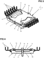
- Fig. 1 shows a power module 1 with a molded body 2 and from the circuit typically encapsulated in the molded body 2 to the outside and preferably of the same size contact pins 3.
- two or more contact pins 3 can also be connected in parallel, or contact pins 3 can be omitted to increase the clearances and creepage distances.
- the semiconductor chips are wired with bonding wires and either with a soft one Cast silicone compound or, in the case of technically more advanced power modules 1 designed as mold modules, hard cast. Due to the hard potting, the bond wires can no longer wobble, so there are no fatigue breaks and the vibration problem is eliminated.
- the contact pins 3 are preferably designed as press-fit pins, with which no tin penetration problems whatsoever as with high-current, lead-free soldered pins occur.
- the contact pins 3 are preferably in two offset rows in order to be able to achieve sufficient distances despite the compact design (pin spacing, for example, only 3 mm).
- the power module 1 can also be used for higher voltages (for example up to 1000VDC)
- Such power modules have a significantly increased reliability and service life compared to conventional power modules. Due to the reduced complexity of the internal structure and manufacturing process, such power modules are also easier and cheaper to manufacture.
- the design of the molded body 2 and the arrangement of the contact pins 3 are preferably the same for all variants of the power module 1, so that a type of “generic housing” is created.
- the design and position of the connections is always the same and the interior can be adapted depending on the task and intended use.
- a power module 1 to be used with the fastening system according to the invention is provided with a molded body 2 which is designed with an essentially flat contact surface 2a for contact with a support structure.
- a molded body 2 which is designed with an essentially flat contact surface 2a for contact with a support structure.
- receptacles 4 are preferably arranged at corners of the power module 1 that are at least symmetrically distributed around the center of the molded body 2.
- the receptacles 4 are preferably arranged in an elevated manner with respect to the central region of the molded body 2. If necessary, a further elevation 6 is preferably arranged in the central area of the shaped body. In relation to the central area of the molded body 2, this preferably reaches a maximum of the height of the receptacles 4. In order not to negatively influence the symmetry of the force introduction into the molded body 2 by the pressing element 5, the further elevation 5 is typically arranged centrally on the molded body 2 .
- the molded body 2 can also be provided with at least one recess 7 on the outer contact pin-free edge area, for example in the form of a semicircular groove or cutout that is open to the outside.
- a through opening with a preferably circular cross-section for the passage of preferably fastening elements or the like could also be present.
- Fig. 2 shows a pressing element 5 according to the invention for use in a fastening system for power modules 1 as described above. It has outer sections 9 starting from a central area 8. These sections 9 merge into outer edge areas 10, which are present in such a geometric arrangement - preferably mirror-symmetrically or point-symmetrically about an axis or the center of the pressure element 5 - that they are in the receptacles 4 when the pressure element 5 is placed on the power module 1 of the shaped body 2 come to rest. If the pressure element 5 is then replaced by suitable connecting elements 11 (see Fig.
- the edge areas 10 are pressed against the receptacles 4 and cause a pressing force on the power module directed through the receptacles 4 towards the supporting structure 1.
- the force is applied in an elastic manner. Due to the exact shape and orientation of the Outwardly facing sections 9 and the outer edge areas 10 of the pressing element 5, the pressing action and the pressing direction can be decoupled to a certain extent from the fastening of the pressing element 5 and the points of application of the pressing force can be selected independently of the fastening points.
- the mode of operation of the fastening system according to the invention is from the Figs. 3 and 4 easy to remove.
- These outer sections 10 are preferably at least partially received in a form-fitting manner and, after the pressing element 5 has been fastened, act elastically on the edge regions of the power module 1 with the receptacles 4.
- the pressing element 5 acts exclusively on the sections of the shaped body 2 that are most curved out of the ideal plane or the contact plane with the support structure or a cooling body, namely on the Corner areas.
- a pressure element 5a that spans several or even all of the lined up power modules 1 can be provided.
- At least one fastening section 13 with a bore 12 for a connecting element 11 is provided in an area between two adjacent power modules 1. In this way, the pressing effect can be transferred evenly to the power modules 1.
- the power modules 1 are configured with the recesses 7 or through openings for the connecting elements 11, the molded bodies 2 can be positioned very close to one another.
- At least the edge regions 9, 10 of the pressing element 5 coming into contact with the power module 1 could be curved towards the power module 1 in order to increase the pressing force if necessary.
- the pressing element 5 is completely flat and has, if at all, a curvature in the form of a bend towards the molded body 2 of the power module 1 only after being braced with the support structure.
- the central elevation 6 on the molded body 2 can be used as a spacer element and / or stop element, as in Fig. 4 can be seen.
- the sections formed on the pressure element 5 can be used as themselves be formed along an edge region of the power module 1, preferably an edge region with contact pins 3, extending edge strips. These edge strips are preferably located on two opposite sides of the pressing element 5 and thus also of the power module 1.
Landscapes
- Engineering & Computer Science (AREA)
- Microelectronics & Electronic Packaging (AREA)
- Cooling Or The Like Of Semiconductors Or Solid State Devices (AREA)
- Inverter Devices (AREA)
Claims (6)
- Élément de pression (5) adapté pour un module de puissance (1), le module de puissance (1) consistant dans un corps moulé (2) pourvu d'une surface d'appui (2a) sensiblement plane, destinée à s'appuyer sur une structure porteuse et dans une multiplicité de broches de contact (3) saillant hors du corps moulé (2), l'élément de pression (5) étant apte à venir en prise sur le corps moulé (2) du module de puissance (1), l'élément de pression (5) pouvant être prévu sur la face du module de puissance (1) qui est opposée à la surface d'appui (2a) et pouvant se fixer sur la structure porteuse du module de puissance (1) à l'aide d'au moins un élément de liaison (11) et pouvant également être soumis à une force de pression en direction de la surface d'appui (2a),
caractérisé en ce que par module de puissance (1), quatre segments (9) extérieurs dont les zones marginales (10) extérieures peuvent agir de manière élastique sur des zones marginales du module de puissance (1), lorsque le module de puissance (1) et l'élément de pression (5) se trouvent en position fixée partent en forme de languettes ou de pattes d'une zone centrale (8) de l'élément de pression (5), les segments extérieurs (9) formés sur l'élément de pression (5) étant conçus sous la forme de bandes marginales s'étendant le long d'une zone marginale du module de puissance (1) avec des broches de contact (3) sur deux faces opposées de l'élément de pression (5) . - Élément de pression selon la revendication 1, caractérisé en ce que des segments de fixation (13) sont conçus sur l'élément de pression (5) sous la forme de pattes saillant par-dessus le module de puissance (1), pourvues de perçages (12) destinés à recevoir des éléments de liaison (11), de préférence des vis.
- Élément de pression selon l'une quelconque des revendications 1 à 2, caractérisé en ce qu'au moins les segments (9, 10) qui viennent en contact avec le module de puissance (1) sont recourbés en direction du module de puissance (1).
- Élément de pression selon l'une quelconque des revendications 1 à 3, caractérisé en ce que l'élément de pression (5a) présente une longueur permettant de venir en prise sur plusieurs modules de puissance (1), au moins un segment de liaison (13) pour au moins un élément de liaison (11) étant conçu dans une zone de l'élément de pression (5) entre deux modules de puissance (1) voisins.
- Système de fixation destiné à un module de puissance (1), consistant dans un corps moulé (2) pourvu d'une surface d'appui (2a) sensiblement plane, destinée à s'appuyer sur une structure porteuse et dans une multiplicité de broches de contact (3) saillant hors du corps moulé (2), avec un élément de pression (5) pour le module de puissance (1), qui vient en prise sur le corps moulé (2) qui est prévu sur une face du module de puissance (1) qui est opposée à la surface d'appui (2a), et avec au moins un élément de liaison (11), destiné à fixer l'élément de pression (5) avec une force de pression en direction de la surface d'appui (2a), caractérisé en ce que l'élément de pression (5) est conçu selon l'une quelconque des revendications 1 à 4, les segments (9) et leurs zones marginales (10) extérieures agissant de manière élastique sur des zones margines du module de puissance (1) et soumettant lesdites zones marginales à une force de pression, lorsque le module de puissance (1) et l'élément de pression (5) se trouvent en position fixée.
- Système de fixation selon la revendication 5, caractérisé en ce que des segments de liaison (13) pour chaque fois au moins un élément de liaison (11) sont prévus sur deux zones marginales opposées de l'élément de pression (5) qui viennent se placer dans la zone d'une zone marginale exempte de broches de contact du module de puissance (1), lorsque le module de puissance (1) et l'élément de pression (5) se trouvent en position fixée.
Priority Applications (2)
| Application Number | Priority Date | Filing Date | Title |
|---|---|---|---|
| EP14163131.7A EP2927954B1 (fr) | 2014-04-02 | 2014-04-02 | Système de fixation pour un module de puissance |
| US14/676,858 US9497876B2 (en) | 2014-04-02 | 2015-04-02 | Fastening systems for power modules |
Applications Claiming Priority (1)
| Application Number | Priority Date | Filing Date | Title |
|---|---|---|---|
| EP14163131.7A EP2927954B1 (fr) | 2014-04-02 | 2014-04-02 | Système de fixation pour un module de puissance |
Publications (2)
| Publication Number | Publication Date |
|---|---|
| EP2927954A1 EP2927954A1 (fr) | 2015-10-07 |
| EP2927954B1 true EP2927954B1 (fr) | 2021-06-09 |
Family
ID=50792349
Family Applications (1)
| Application Number | Title | Priority Date | Filing Date |
|---|---|---|---|
| EP14163131.7A Active EP2927954B1 (fr) | 2014-04-02 | 2014-04-02 | Système de fixation pour un module de puissance |
Country Status (2)
| Country | Link |
|---|---|
| US (1) | US9497876B2 (fr) |
| EP (1) | EP2927954B1 (fr) |
Families Citing this family (2)
| Publication number | Priority date | Publication date | Assignee | Title |
|---|---|---|---|---|
| EP2927954B1 (fr) | 2014-04-02 | 2021-06-09 | Brusa Elektronik AG | Système de fixation pour un module de puissance |
| CN106572621B (zh) * | 2016-11-10 | 2018-12-21 | 广东高标电子科技有限公司 | 控制器以及具有该控制器的电动车 |
Citations (1)
| Publication number | Priority date | Publication date | Assignee | Title |
|---|---|---|---|---|
| US20100127391A1 (en) * | 2008-11-21 | 2010-05-27 | Tsuyoshi Hasegawa | Fixture for semiconductor device and assembly of semiconductor device |
Family Cites Families (12)
| Publication number | Priority date | Publication date | Assignee | Title |
|---|---|---|---|---|
| JPS5963735A (ja) | 1982-10-05 | 1984-04-11 | Rohm Co Ltd | 半導体装置の製造方法 |
| JPS5999743A (ja) * | 1982-11-30 | 1984-06-08 | Nissan Motor Co Ltd | 集積回路パツケ−ジ |
| DE59406013D1 (de) * | 1993-06-07 | 1998-06-25 | Melcher Ag | Befestigungsvorrichtung für halbleiter-schaltelemente |
| JPH09199645A (ja) | 1996-01-17 | 1997-07-31 | Mitsubishi Electric Corp | 半導体装置および半導体モジュール |
| JP3725103B2 (ja) * | 2002-08-23 | 2005-12-07 | 三菱電機株式会社 | 半導体装置 |
| JP4387777B2 (ja) * | 2003-11-28 | 2009-12-24 | 株式会社東芝 | 電子機器 |
| US20060139890A1 (en) * | 2004-12-23 | 2006-06-29 | A-Sheng Liu | Fastening device II |
| DE102007020618B8 (de) | 2007-04-30 | 2009-03-12 | Danfoss Silicon Power Gmbh | Verfahren zum Herstellen eines festen Leistungsmoduls und damit hergestelltes Transistormodul |
| US8120171B2 (en) * | 2007-12-26 | 2012-02-21 | Keihin Corporation | Power drive unit including a heat sink and a fastener |
| FR2931523B1 (fr) * | 2008-05-21 | 2013-01-04 | Fagorbrandt Sas | Dispositif de fixation de composants et appareil electromenager associe |
| JP2011035265A (ja) * | 2009-08-04 | 2011-02-17 | Mitsubishi Electric Corp | 半導体装置 |
| EP2927954B1 (fr) | 2014-04-02 | 2021-06-09 | Brusa Elektronik AG | Système de fixation pour un module de puissance |
-
2014
- 2014-04-02 EP EP14163131.7A patent/EP2927954B1/fr active Active
-
2015
- 2015-04-02 US US14/676,858 patent/US9497876B2/en active Active
Patent Citations (1)
| Publication number | Priority date | Publication date | Assignee | Title |
|---|---|---|---|---|
| US20100127391A1 (en) * | 2008-11-21 | 2010-05-27 | Tsuyoshi Hasegawa | Fixture for semiconductor device and assembly of semiconductor device |
Also Published As
| Publication number | Publication date |
|---|---|
| US9497876B2 (en) | 2016-11-15 |
| US20150289404A1 (en) | 2015-10-08 |
| EP2927954A1 (fr) | 2015-10-07 |
Similar Documents
| Publication | Publication Date | Title |
|---|---|---|
| DE112007002446B4 (de) | Elektronische Schaltungsvorrichtung und Verfahren zu ihrer Herstellung | |
| DE102011089539B3 (de) | Vorrichtung zur Ansteuerung einer elektrischen Heizung für Fahrzeuge und elektrische Heizung mit einer derartigen Vorrichtung | |
| DE102009002992B4 (de) | Leistungshalbleitermodulanordnung mit eindeutig und verdrehsicher auf einem Kühlkörper montierbarem Leistungshalbleitermodul und Montageverfahren | |
| DE10149886A1 (de) | Leistunghalbleitermodul | |
| DE112011105738B4 (de) | Halbleitermodul | |
| DE102011075921B4 (de) | Mittels Klemmkeil und Gegenkeil elektrisch anschließbares Leistungshalbeiitermodul und Leistungshalbleitermodulsystem mit einem solchen Leistungshalbleitermodul | |
| DE10324909A1 (de) | Gehäuse für ein strahlungsemittierendes Bauelement, Verfahren zu dessen Herstellung und strahlungsemittierendes Bauelement | |
| DE112016005240B4 (de) | Schaltungsanordnung und elektrischer Verteilerkasten | |
| DE102014217266B4 (de) | Halbleitervorrichtung | |
| DE112011105754B4 (de) | Halbleitermodul | |
| EP2927954B1 (fr) | Système de fixation pour un module de puissance | |
| EP1787325B1 (fr) | Construction modulaire | |
| EP2305010B1 (fr) | Montage de circuits électriques | |
| DE102016106180A1 (de) | Kühlvorrichtung für die Kühlung wenigstens einer elektrischen Komponente eines Fahrzeugs | |
| EP3499563B1 (fr) | Module semi-conducteur de puissance et procédé de positionnement en force d'un module semi-conducteur de puissance | |
| DE202014003171U1 (de) | Leistungshalbleitermodul | |
| DE102012101666B3 (de) | Leistungshalbleitermodulsystem mit Hinterschneidungsverbindung | |
| DE102010003466A1 (de) | Verbindungselement, elektrischer Verbinder und Verbindungsanordnung für Solarzellenmodule | |
| DE29511775U1 (de) | Anordnung mit einer Leiterplatte | |
| DE112019002508T5 (de) | Schaltungseinrichtung | |
| DE102017218875A1 (de) | Leistungsmodul mit Merkmalen zum Klemmen und Leistungsmodul-Baugruppe | |
| WO2012113584A1 (fr) | Module à semi-conducteur de puissance | |
| DE102011075515B4 (de) | Verbessertes Leistungshalbleiterbauelementmodul | |
| EP1921909B1 (fr) | Module de puissance | |
| DE102012206407B4 (de) | Druckkontaktanordnung und verfahren zur herstellung und zum betrieb einer druckkontaktanordnung |
Legal Events
| Date | Code | Title | Description |
|---|---|---|---|
| PUAI | Public reference made under article 153(3) epc to a published international application that has entered the european phase |
Free format text: ORIGINAL CODE: 0009012 |
|
| AK | Designated contracting states |
Kind code of ref document: A1 Designated state(s): AL AT BE BG CH CY CZ DE DK EE ES FI FR GB GR HR HU IE IS IT LI LT LU LV MC MK MT NL NO PL PT RO RS SE SI SK SM TR |
|
| AX | Request for extension of the european patent |
Extension state: BA ME |
|
| 17P | Request for examination filed |
Effective date: 20160316 |
|
| RBV | Designated contracting states (corrected) |
Designated state(s): AL AT BE BG CH CY CZ DE DK EE ES FI FR GB GR HR HU IE IS IT LI LT LU LV MC MK MT NL NO PL PT RO RS SE SI SK SM TR |
|
| STAA | Information on the status of an ep patent application or granted ep patent |
Free format text: STATUS: EXAMINATION IS IN PROGRESS |
|
| 17Q | First examination report despatched |
Effective date: 20161115 |
|
| REG | Reference to a national code |
Ref country code: DE Ref legal event code: R079 Ref document number: 502014015649 Country of ref document: DE Free format text: PREVIOUS MAIN CLASS: H01L0023400000 Ipc: H01L0023000000 |
|
| RIC1 | Information provided on ipc code assigned before grant |
Ipc: H01L 23/40 20060101ALI20191126BHEP Ipc: H01L 23/00 20060101AFI20191126BHEP Ipc: H05K 7/02 20060101ALI20191126BHEP Ipc: H01L 25/065 20060101ALI20191126BHEP Ipc: H01L 25/11 20060101ALI20191126BHEP Ipc: H01L 23/31 20060101ALI20191126BHEP |
|
| GRAP | Despatch of communication of intention to grant a patent |
Free format text: ORIGINAL CODE: EPIDOSNIGR1 |
|
| STAA | Information on the status of an ep patent application or granted ep patent |
Free format text: STATUS: GRANT OF PATENT IS INTENDED |
|
| INTG | Intention to grant announced |
Effective date: 20210122 |
|
| GRAS | Grant fee paid |
Free format text: ORIGINAL CODE: EPIDOSNIGR3 |
|
| GRAA | (expected) grant |
Free format text: ORIGINAL CODE: 0009210 |
|
| STAA | Information on the status of an ep patent application or granted ep patent |
Free format text: STATUS: THE PATENT HAS BEEN GRANTED |
|
| AK | Designated contracting states |
Kind code of ref document: B1 Designated state(s): AL AT BE BG CH CY CZ DE DK EE ES FI FR GB GR HR HU IE IS IT LI LT LU LV MC MK MT NL NO PL PT RO RS SE SI SK SM TR |
|
| REG | Reference to a national code |
Ref country code: GB Ref legal event code: FG4D Free format text: NOT ENGLISH |
|
| REG | Reference to a national code |
Ref country code: CH Ref legal event code: EP Ref country code: AT Ref legal event code: REF Ref document number: 1401188 Country of ref document: AT Kind code of ref document: T Effective date: 20210615 |
|
| REG | Reference to a national code |
Ref country code: DE Ref legal event code: R096 Ref document number: 502014015649 Country of ref document: DE |
|
| REG | Reference to a national code |
Ref country code: IE Ref legal event code: FG4D Free format text: LANGUAGE OF EP DOCUMENT: GERMAN |
|
| REG | Reference to a national code |
Ref country code: LT Ref legal event code: MG9D |
|
| PG25 | Lapsed in a contracting state [announced via postgrant information from national office to epo] |
Ref country code: LT Free format text: LAPSE BECAUSE OF FAILURE TO SUBMIT A TRANSLATION OF THE DESCRIPTION OR TO PAY THE FEE WITHIN THE PRESCRIBED TIME-LIMIT Effective date: 20210609 Ref country code: FI Free format text: LAPSE BECAUSE OF FAILURE TO SUBMIT A TRANSLATION OF THE DESCRIPTION OR TO PAY THE FEE WITHIN THE PRESCRIBED TIME-LIMIT Effective date: 20210609 Ref country code: BG Free format text: LAPSE BECAUSE OF FAILURE TO SUBMIT A TRANSLATION OF THE DESCRIPTION OR TO PAY THE FEE WITHIN THE PRESCRIBED TIME-LIMIT Effective date: 20210909 Ref country code: HR Free format text: LAPSE BECAUSE OF FAILURE TO SUBMIT A TRANSLATION OF THE DESCRIPTION OR TO PAY THE FEE WITHIN THE PRESCRIBED TIME-LIMIT Effective date: 20210609 |
|
| REG | Reference to a national code |
Ref country code: NL Ref legal event code: MP Effective date: 20210609 |
|
| PG25 | Lapsed in a contracting state [announced via postgrant information from national office to epo] |
Ref country code: NO Free format text: LAPSE BECAUSE OF FAILURE TO SUBMIT A TRANSLATION OF THE DESCRIPTION OR TO PAY THE FEE WITHIN THE PRESCRIBED TIME-LIMIT Effective date: 20210909 Ref country code: RS Free format text: LAPSE BECAUSE OF FAILURE TO SUBMIT A TRANSLATION OF THE DESCRIPTION OR TO PAY THE FEE WITHIN THE PRESCRIBED TIME-LIMIT Effective date: 20210609 Ref country code: SE Free format text: LAPSE BECAUSE OF FAILURE TO SUBMIT A TRANSLATION OF THE DESCRIPTION OR TO PAY THE FEE WITHIN THE PRESCRIBED TIME-LIMIT Effective date: 20210609 Ref country code: LV Free format text: LAPSE BECAUSE OF FAILURE TO SUBMIT A TRANSLATION OF THE DESCRIPTION OR TO PAY THE FEE WITHIN THE PRESCRIBED TIME-LIMIT Effective date: 20210609 Ref country code: GR Free format text: LAPSE BECAUSE OF FAILURE TO SUBMIT A TRANSLATION OF THE DESCRIPTION OR TO PAY THE FEE WITHIN THE PRESCRIBED TIME-LIMIT Effective date: 20210910 |
|
| PG25 | Lapsed in a contracting state [announced via postgrant information from national office to epo] |
Ref country code: SK Free format text: LAPSE BECAUSE OF FAILURE TO SUBMIT A TRANSLATION OF THE DESCRIPTION OR TO PAY THE FEE WITHIN THE PRESCRIBED TIME-LIMIT Effective date: 20210609 Ref country code: SM Free format text: LAPSE BECAUSE OF FAILURE TO SUBMIT A TRANSLATION OF THE DESCRIPTION OR TO PAY THE FEE WITHIN THE PRESCRIBED TIME-LIMIT Effective date: 20210609 Ref country code: CZ Free format text: LAPSE BECAUSE OF FAILURE TO SUBMIT A TRANSLATION OF THE DESCRIPTION OR TO PAY THE FEE WITHIN THE PRESCRIBED TIME-LIMIT Effective date: 20210609 Ref country code: EE Free format text: LAPSE BECAUSE OF FAILURE TO SUBMIT A TRANSLATION OF THE DESCRIPTION OR TO PAY THE FEE WITHIN THE PRESCRIBED TIME-LIMIT Effective date: 20210609 Ref country code: RO Free format text: LAPSE BECAUSE OF FAILURE TO SUBMIT A TRANSLATION OF THE DESCRIPTION OR TO PAY THE FEE WITHIN THE PRESCRIBED TIME-LIMIT Effective date: 20210609 Ref country code: NL Free format text: LAPSE BECAUSE OF FAILURE TO SUBMIT A TRANSLATION OF THE DESCRIPTION OR TO PAY THE FEE WITHIN THE PRESCRIBED TIME-LIMIT Effective date: 20210609 Ref country code: PT Free format text: LAPSE BECAUSE OF FAILURE TO SUBMIT A TRANSLATION OF THE DESCRIPTION OR TO PAY THE FEE WITHIN THE PRESCRIBED TIME-LIMIT Effective date: 20211011 Ref country code: ES Free format text: LAPSE BECAUSE OF FAILURE TO SUBMIT A TRANSLATION OF THE DESCRIPTION OR TO PAY THE FEE WITHIN THE PRESCRIBED TIME-LIMIT Effective date: 20210609 |
|
| PG25 | Lapsed in a contracting state [announced via postgrant information from national office to epo] |
Ref country code: PL Free format text: LAPSE BECAUSE OF FAILURE TO SUBMIT A TRANSLATION OF THE DESCRIPTION OR TO PAY THE FEE WITHIN THE PRESCRIBED TIME-LIMIT Effective date: 20210609 |
|
| REG | Reference to a national code |
Ref country code: DE Ref legal event code: R097 Ref document number: 502014015649 Country of ref document: DE |
|
| PLBE | No opposition filed within time limit |
Free format text: ORIGINAL CODE: 0009261 |
|
| STAA | Information on the status of an ep patent application or granted ep patent |
Free format text: STATUS: NO OPPOSITION FILED WITHIN TIME LIMIT |
|
| PG25 | Lapsed in a contracting state [announced via postgrant information from national office to epo] |
Ref country code: DK Free format text: LAPSE BECAUSE OF FAILURE TO SUBMIT A TRANSLATION OF THE DESCRIPTION OR TO PAY THE FEE WITHIN THE PRESCRIBED TIME-LIMIT Effective date: 20210609 |
|
| 26N | No opposition filed |
Effective date: 20220310 |
|
| PG25 | Lapsed in a contracting state [announced via postgrant information from national office to epo] |
Ref country code: AL Free format text: LAPSE BECAUSE OF FAILURE TO SUBMIT A TRANSLATION OF THE DESCRIPTION OR TO PAY THE FEE WITHIN THE PRESCRIBED TIME-LIMIT Effective date: 20210609 |
|
| REG | Reference to a national code |
Ref country code: CH Ref legal event code: PL |
|
| REG | Reference to a national code |
Ref country code: BE Ref legal event code: MM Effective date: 20220430 |
|
| PG25 | Lapsed in a contracting state [announced via postgrant information from national office to epo] |
Ref country code: MC Free format text: LAPSE BECAUSE OF FAILURE TO SUBMIT A TRANSLATION OF THE DESCRIPTION OR TO PAY THE FEE WITHIN THE PRESCRIBED TIME-LIMIT Effective date: 20210609 Ref country code: LU Free format text: LAPSE BECAUSE OF NON-PAYMENT OF DUE FEES Effective date: 20220402 Ref country code: LI Free format text: LAPSE BECAUSE OF NON-PAYMENT OF DUE FEES Effective date: 20220430 Ref country code: CH Free format text: LAPSE BECAUSE OF NON-PAYMENT OF DUE FEES Effective date: 20220430 |
|
| PG25 | Lapsed in a contracting state [announced via postgrant information from national office to epo] |
Ref country code: BE Free format text: LAPSE BECAUSE OF NON-PAYMENT OF DUE FEES Effective date: 20220430 |
|
| PG25 | Lapsed in a contracting state [announced via postgrant information from national office to epo] |
Ref country code: IE Free format text: LAPSE BECAUSE OF NON-PAYMENT OF DUE FEES Effective date: 20220402 |
|
| REG | Reference to a national code |
Ref country code: AT Ref legal event code: MM01 Ref document number: 1401188 Country of ref document: AT Kind code of ref document: T Effective date: 20220402 |
|
| PG25 | Lapsed in a contracting state [announced via postgrant information from national office to epo] |
Ref country code: AT Free format text: LAPSE BECAUSE OF NON-PAYMENT OF DUE FEES Effective date: 20220402 |
|
| REG | Reference to a national code |
Ref country code: DE Ref legal event code: R081 Ref document number: 502014015649 Country of ref document: DE Owner name: BRUSA TECHNOLOGY AG, CH Free format text: FORMER OWNER: BRUSA ELEKTRONIK AG, SENNWALD, CH |
|
| REG | Reference to a national code |
Ref country code: GB Ref legal event code: 732E Free format text: REGISTERED BETWEEN 20231102 AND 20231108 |
|
| PG25 | Lapsed in a contracting state [announced via postgrant information from national office to epo] |
Ref country code: HU Free format text: LAPSE BECAUSE OF FAILURE TO SUBMIT A TRANSLATION OF THE DESCRIPTION OR TO PAY THE FEE WITHIN THE PRESCRIBED TIME-LIMIT; INVALID AB INITIO Effective date: 20140402 |
|
| PG25 | Lapsed in a contracting state [announced via postgrant information from national office to epo] |
Ref country code: MK Free format text: LAPSE BECAUSE OF FAILURE TO SUBMIT A TRANSLATION OF THE DESCRIPTION OR TO PAY THE FEE WITHIN THE PRESCRIBED TIME-LIMIT Effective date: 20210609 Ref country code: CY Free format text: LAPSE BECAUSE OF FAILURE TO SUBMIT A TRANSLATION OF THE DESCRIPTION OR TO PAY THE FEE WITHIN THE PRESCRIBED TIME-LIMIT Effective date: 20210609 |
|
| PG25 | Lapsed in a contracting state [announced via postgrant information from national office to epo] |
Ref country code: MT Free format text: LAPSE BECAUSE OF FAILURE TO SUBMIT A TRANSLATION OF THE DESCRIPTION OR TO PAY THE FEE WITHIN THE PRESCRIBED TIME-LIMIT Effective date: 20210609 |
|
| PGFP | Annual fee paid to national office [announced via postgrant information from national office to epo] |
Ref country code: DE Payment date: 20250423 Year of fee payment: 12 |
|
| PGFP | Annual fee paid to national office [announced via postgrant information from national office to epo] |
Ref country code: GB Payment date: 20250423 Year of fee payment: 12 |
|
| PGFP | Annual fee paid to national office [announced via postgrant information from national office to epo] |
Ref country code: IT Payment date: 20250430 Year of fee payment: 12 |
|
| PGFP | Annual fee paid to national office [announced via postgrant information from national office to epo] |
Ref country code: FR Payment date: 20250422 Year of fee payment: 12 |
|
| REG | Reference to a national code |
Ref country code: DE Ref legal event code: R079 Ref document number: 502014015649 Country of ref document: DE Free format text: PREVIOUS MAIN CLASS: H01L0023000000 Ipc: H10W0099000000 |
|
| PG25 | Lapsed in a contracting state [announced via postgrant information from national office to epo] |
Ref country code: TR Free format text: LAPSE BECAUSE OF FAILURE TO SUBMIT A TRANSLATION OF THE DESCRIPTION OR TO PAY THE FEE WITHIN THE PRESCRIBED TIME-LIMIT Effective date: 20210609 |