EP2980048A1 - Appareil et procédé de production de stratifié (plaque métallique)-(plaque céramique) et appareil et procédé de production de substrat pour des modules de puissance - Google Patents
Appareil et procédé de production de stratifié (plaque métallique)-(plaque céramique) et appareil et procédé de production de substrat pour des modules de puissance Download PDFInfo
- Publication number
- EP2980048A1 EP2980048A1 EP14774133.4A EP14774133A EP2980048A1 EP 2980048 A1 EP2980048 A1 EP 2980048A1 EP 14774133 A EP14774133 A EP 14774133A EP 2980048 A1 EP2980048 A1 EP 2980048A1
- Authority
- EP
- European Patent Office
- Prior art keywords
- ceramic board
- metal plate
- plate
- bonding
- temporary
- Prior art date
- Legal status (The legal status is an assumption and is not a legal conclusion. Google has not performed a legal analysis and makes no representation as to the accuracy of the status listed.)
- Granted
Links
Images


Classifications
-
- C—CHEMISTRY; METALLURGY
- C04—CEMENTS; CONCRETE; ARTIFICIAL STONE; CERAMICS; REFRACTORIES
- C04B—LIME, MAGNESIA; SLAG; CEMENTS; COMPOSITIONS THEREOF, e.g. MORTARS, CONCRETE OR LIKE BUILDING MATERIALS; ARTIFICIAL STONE; CERAMICS; REFRACTORIES; TREATMENT OF NATURAL STONE
- C04B37/00—Joining burned ceramic articles with other burned ceramic articles or other articles by heating
- C04B37/02—Joining burned ceramic articles with other burned ceramic articles or other articles by heating with metallic articles
- C04B37/023—Joining burned ceramic articles with other burned ceramic articles or other articles by heating with metallic articles characterised by the interlayer used
- C04B37/026—Joining burned ceramic articles with other burned ceramic articles or other articles by heating with metallic articles characterised by the interlayer used consisting of metals or metal salts
-
- B—PERFORMING OPERATIONS; TRANSPORTING
- B23—MACHINE TOOLS; METAL-WORKING NOT OTHERWISE PROVIDED FOR
- B23K—SOLDERING OR UNSOLDERING; WELDING; CLADDING OR PLATING BY SOLDERING OR WELDING; CUTTING BY APPLYING HEAT LOCALLY, e.g. FLAME CUTTING; WORKING BY LASER BEAM
- B23K1/00—Soldering, e.g. brazing, or unsoldering
- B23K1/0008—Soldering, e.g. brazing, or unsoldering specially adapted for particular articles or work
- B23K1/0016—Soldering of electronic components
-
- B—PERFORMING OPERATIONS; TRANSPORTING
- B23—MACHINE TOOLS; METAL-WORKING NOT OTHERWISE PROVIDED FOR
- B23K—SOLDERING OR UNSOLDERING; WELDING; CLADDING OR PLATING BY SOLDERING OR WELDING; CUTTING BY APPLYING HEAT LOCALLY, e.g. FLAME CUTTING; WORKING BY LASER BEAM
- B23K1/00—Soldering, e.g. brazing, or unsoldering
- B23K1/19—Soldering, e.g. brazing, or unsoldering taking account of the properties of the materials to be soldered
-
- H—ELECTRICITY
- H05—ELECTRIC TECHNIQUES NOT OTHERWISE PROVIDED FOR
- H05K—PRINTED CIRCUITS; CASINGS OR CONSTRUCTIONAL DETAILS OF ELECTRIC APPARATUS; MANUFACTURE OF ASSEMBLAGES OF ELECTRICAL COMPONENTS
- H05K3/00—Apparatus or processes for manufacturing printed circuits
- H05K3/0058—Laminating printed circuit boards onto other substrates, e.g. metallic substrates
- H05K3/0061—Laminating printed circuit boards onto other substrates, e.g. metallic substrates onto a metallic substrate, e.g. a heat sink
-
- H—ELECTRICITY
- H05—ELECTRIC TECHNIQUES NOT OTHERWISE PROVIDED FOR
- H05K—PRINTED CIRCUITS; CASINGS OR CONSTRUCTIONAL DETAILS OF ELECTRIC APPARATUS; MANUFACTURE OF ASSEMBLAGES OF ELECTRICAL COMPONENTS
- H05K3/00—Apparatus or processes for manufacturing printed circuits
- H05K3/02—Apparatus or processes for manufacturing printed circuits in which the conductive material is applied to the surface of the insulating support and is thereafter removed from such areas of the surface which are not intended for current conducting or shielding
- H05K3/022—Processes for manufacturing precursors of printed circuits, i.e. copper-clad substrates
-
- H—ELECTRICITY
- H10—SEMICONDUCTOR DEVICES; ELECTRIC SOLID-STATE DEVICES NOT OTHERWISE PROVIDED FOR
- H10P—GENERIC PROCESSES OR APPARATUS FOR THE MANUFACTURE OR TREATMENT OF DEVICES COVERED BY CLASS H10
- H10P72/00—Handling or holding of wafers, substrates or devices during manufacture or treatment thereof
- H10P72/04—Apparatus for manufacture or treatment
- H10P72/0431—Apparatus for thermal treatment
- H10P72/0434—Apparatus for thermal treatment mainly by convection
-
- H—ELECTRICITY
- H10—SEMICONDUCTOR DEVICES; ELECTRIC SOLID-STATE DEVICES NOT OTHERWISE PROVIDED FOR
- H10P—GENERIC PROCESSES OR APPARATUS FOR THE MANUFACTURE OR TREATMENT OF DEVICES COVERED BY CLASS H10
- H10P72/00—Handling or holding of wafers, substrates or devices during manufacture or treatment thereof
- H10P72/04—Apparatus for manufacture or treatment
- H10P72/0446—Apparatus for mounting on conductive members, e.g. leadframes or conductors on insulating substrates
-
- H—ELECTRICITY
- H10—SEMICONDUCTOR DEVICES; ELECTRIC SOLID-STATE DEVICES NOT OTHERWISE PROVIDED FOR
- H10P—GENERIC PROCESSES OR APPARATUS FOR THE MANUFACTURE OR TREATMENT OF DEVICES COVERED BY CLASS H10
- H10P72/00—Handling or holding of wafers, substrates or devices during manufacture or treatment thereof
- H10P72/06—Apparatus for monitoring, sorting, marking, testing or measuring
- H10P72/0602—Temperature monitoring
-
- H—ELECTRICITY
- H10—SEMICONDUCTOR DEVICES; ELECTRIC SOLID-STATE DEVICES NOT OTHERWISE PROVIDED FOR
- H10P—GENERIC PROCESSES OR APPARATUS FOR THE MANUFACTURE OR TREATMENT OF DEVICES COVERED BY CLASS H10
- H10P72/00—Handling or holding of wafers, substrates or devices during manufacture or treatment thereof
- H10P72/30—Handling or holding of wafers, substrates or devices during manufacture or treatment thereof for conveying, e.g. between different workstations
-
- H—ELECTRICITY
- H10—SEMICONDUCTOR DEVICES; ELECTRIC SOLID-STATE DEVICES NOT OTHERWISE PROVIDED FOR
- H10W—GENERIC PACKAGES, INTERCONNECTIONS, CONNECTORS OR OTHER CONSTRUCTIONAL DETAILS OF DEVICES COVERED BY CLASS H10
- H10W40/00—Arrangements for thermal protection or thermal control
- H10W40/01—Manufacture or treatment
- H10W40/03—Manufacture or treatment of arrangements for cooling
- H10W40/037—Assembling together parts thereof
-
- H—ELECTRICITY
- H10—SEMICONDUCTOR DEVICES; ELECTRIC SOLID-STATE DEVICES NOT OTHERWISE PROVIDED FOR
- H10W—GENERIC PACKAGES, INTERCONNECTIONS, CONNECTORS OR OTHER CONSTRUCTIONAL DETAILS OF DEVICES COVERED BY CLASS H10
- H10W40/00—Arrangements for thermal protection or thermal control
- H10W40/20—Arrangements for cooling
- H10W40/25—Arrangements for cooling characterised by their materials
- H10W40/255—Arrangements for cooling characterised by their materials having a laminate or multilayered structure, e.g. direct bond copper [DBC] ceramic substrates
-
- C—CHEMISTRY; METALLURGY
- C04—CEMENTS; CONCRETE; ARTIFICIAL STONE; CERAMICS; REFRACTORIES
- C04B—LIME, MAGNESIA; SLAG; CEMENTS; COMPOSITIONS THEREOF, e.g. MORTARS, CONCRETE OR LIKE BUILDING MATERIALS; ARTIFICIAL STONE; CERAMICS; REFRACTORIES; TREATMENT OF NATURAL STONE
- C04B2237/00—Aspects relating to ceramic laminates or to joining of ceramic articles with other articles by heating
- C04B2237/02—Aspects relating to interlayers, e.g. used to join ceramic articles with other articles by heating
- C04B2237/12—Metallic interlayers
- C04B2237/121—Metallic interlayers based on aluminium
-
- C—CHEMISTRY; METALLURGY
- C04—CEMENTS; CONCRETE; ARTIFICIAL STONE; CERAMICS; REFRACTORIES
- C04B—LIME, MAGNESIA; SLAG; CEMENTS; COMPOSITIONS THEREOF, e.g. MORTARS, CONCRETE OR LIKE BUILDING MATERIALS; ARTIFICIAL STONE; CERAMICS; REFRACTORIES; TREATMENT OF NATURAL STONE
- C04B2237/00—Aspects relating to ceramic laminates or to joining of ceramic articles with other articles by heating
- C04B2237/02—Aspects relating to interlayers, e.g. used to join ceramic articles with other articles by heating
- C04B2237/12—Metallic interlayers
- C04B2237/125—Metallic interlayers based on noble metals, e.g. silver
-
- C—CHEMISTRY; METALLURGY
- C04—CEMENTS; CONCRETE; ARTIFICIAL STONE; CERAMICS; REFRACTORIES
- C04B—LIME, MAGNESIA; SLAG; CEMENTS; COMPOSITIONS THEREOF, e.g. MORTARS, CONCRETE OR LIKE BUILDING MATERIALS; ARTIFICIAL STONE; CERAMICS; REFRACTORIES; TREATMENT OF NATURAL STONE
- C04B2237/00—Aspects relating to ceramic laminates or to joining of ceramic articles with other articles by heating
- C04B2237/02—Aspects relating to interlayers, e.g. used to join ceramic articles with other articles by heating
- C04B2237/12—Metallic interlayers
- C04B2237/126—Metallic interlayers wherein the active component for bonding is not the largest fraction of the interlayer
- C04B2237/127—The active component for bonding being a refractory metal
-
- C—CHEMISTRY; METALLURGY
- C04—CEMENTS; CONCRETE; ARTIFICIAL STONE; CERAMICS; REFRACTORIES
- C04B—LIME, MAGNESIA; SLAG; CEMENTS; COMPOSITIONS THEREOF, e.g. MORTARS, CONCRETE OR LIKE BUILDING MATERIALS; ARTIFICIAL STONE; CERAMICS; REFRACTORIES; TREATMENT OF NATURAL STONE
- C04B2237/00—Aspects relating to ceramic laminates or to joining of ceramic articles with other articles by heating
- C04B2237/02—Aspects relating to interlayers, e.g. used to join ceramic articles with other articles by heating
- C04B2237/12—Metallic interlayers
- C04B2237/126—Metallic interlayers wherein the active component for bonding is not the largest fraction of the interlayer
- C04B2237/128—The active component for bonding being silicon
-
- C—CHEMISTRY; METALLURGY
- C04—CEMENTS; CONCRETE; ARTIFICIAL STONE; CERAMICS; REFRACTORIES
- C04B—LIME, MAGNESIA; SLAG; CEMENTS; COMPOSITIONS THEREOF, e.g. MORTARS, CONCRETE OR LIKE BUILDING MATERIALS; ARTIFICIAL STONE; CERAMICS; REFRACTORIES; TREATMENT OF NATURAL STONE
- C04B2237/00—Aspects relating to ceramic laminates or to joining of ceramic articles with other articles by heating
- C04B2237/30—Composition of layers of ceramic laminates or of ceramic or metallic articles to be joined by heating, e.g. Si substrates
- C04B2237/32—Ceramic
- C04B2237/34—Oxidic
- C04B2237/343—Alumina or aluminates
-
- C—CHEMISTRY; METALLURGY
- C04—CEMENTS; CONCRETE; ARTIFICIAL STONE; CERAMICS; REFRACTORIES
- C04B—LIME, MAGNESIA; SLAG; CEMENTS; COMPOSITIONS THEREOF, e.g. MORTARS, CONCRETE OR LIKE BUILDING MATERIALS; ARTIFICIAL STONE; CERAMICS; REFRACTORIES; TREATMENT OF NATURAL STONE
- C04B2237/00—Aspects relating to ceramic laminates or to joining of ceramic articles with other articles by heating
- C04B2237/30—Composition of layers of ceramic laminates or of ceramic or metallic articles to be joined by heating, e.g. Si substrates
- C04B2237/32—Ceramic
- C04B2237/36—Non-oxidic
- C04B2237/366—Aluminium nitride
-
- C—CHEMISTRY; METALLURGY
- C04—CEMENTS; CONCRETE; ARTIFICIAL STONE; CERAMICS; REFRACTORIES
- C04B—LIME, MAGNESIA; SLAG; CEMENTS; COMPOSITIONS THEREOF, e.g. MORTARS, CONCRETE OR LIKE BUILDING MATERIALS; ARTIFICIAL STONE; CERAMICS; REFRACTORIES; TREATMENT OF NATURAL STONE
- C04B2237/00—Aspects relating to ceramic laminates or to joining of ceramic articles with other articles by heating
- C04B2237/30—Composition of layers of ceramic laminates or of ceramic or metallic articles to be joined by heating, e.g. Si substrates
- C04B2237/32—Ceramic
- C04B2237/36—Non-oxidic
- C04B2237/368—Silicon nitride
-
- C—CHEMISTRY; METALLURGY
- C04—CEMENTS; CONCRETE; ARTIFICIAL STONE; CERAMICS; REFRACTORIES
- C04B—LIME, MAGNESIA; SLAG; CEMENTS; COMPOSITIONS THEREOF, e.g. MORTARS, CONCRETE OR LIKE BUILDING MATERIALS; ARTIFICIAL STONE; CERAMICS; REFRACTORIES; TREATMENT OF NATURAL STONE
- C04B2237/00—Aspects relating to ceramic laminates or to joining of ceramic articles with other articles by heating
- C04B2237/30—Composition of layers of ceramic laminates or of ceramic or metallic articles to be joined by heating, e.g. Si substrates
- C04B2237/40—Metallic
- C04B2237/402—Aluminium
-
- C—CHEMISTRY; METALLURGY
- C04—CEMENTS; CONCRETE; ARTIFICIAL STONE; CERAMICS; REFRACTORIES
- C04B—LIME, MAGNESIA; SLAG; CEMENTS; COMPOSITIONS THEREOF, e.g. MORTARS, CONCRETE OR LIKE BUILDING MATERIALS; ARTIFICIAL STONE; CERAMICS; REFRACTORIES; TREATMENT OF NATURAL STONE
- C04B2237/00—Aspects relating to ceramic laminates or to joining of ceramic articles with other articles by heating
- C04B2237/30—Composition of layers of ceramic laminates or of ceramic or metallic articles to be joined by heating, e.g. Si substrates
- C04B2237/40—Metallic
- C04B2237/407—Copper
-
- C—CHEMISTRY; METALLURGY
- C04—CEMENTS; CONCRETE; ARTIFICIAL STONE; CERAMICS; REFRACTORIES
- C04B—LIME, MAGNESIA; SLAG; CEMENTS; COMPOSITIONS THEREOF, e.g. MORTARS, CONCRETE OR LIKE BUILDING MATERIALS; ARTIFICIAL STONE; CERAMICS; REFRACTORIES; TREATMENT OF NATURAL STONE
- C04B2237/00—Aspects relating to ceramic laminates or to joining of ceramic articles with other articles by heating
- C04B2237/50—Processing aspects relating to ceramic laminates or to the joining of ceramic articles with other articles by heating
- C04B2237/70—Forming laminates or joined articles comprising layers of a specific, unusual thickness
- C04B2237/704—Forming laminates or joined articles comprising layers of a specific, unusual thickness of one or more of the ceramic layers or articles
-
- C—CHEMISTRY; METALLURGY
- C04—CEMENTS; CONCRETE; ARTIFICIAL STONE; CERAMICS; REFRACTORIES
- C04B—LIME, MAGNESIA; SLAG; CEMENTS; COMPOSITIONS THEREOF, e.g. MORTARS, CONCRETE OR LIKE BUILDING MATERIALS; ARTIFICIAL STONE; CERAMICS; REFRACTORIES; TREATMENT OF NATURAL STONE
- C04B2237/00—Aspects relating to ceramic laminates or to joining of ceramic articles with other articles by heating
- C04B2237/50—Processing aspects relating to ceramic laminates or to the joining of ceramic articles with other articles by heating
- C04B2237/70—Forming laminates or joined articles comprising layers of a specific, unusual thickness
- C04B2237/706—Forming laminates or joined articles comprising layers of a specific, unusual thickness of one or more of the metallic layers or articles
-
- C—CHEMISTRY; METALLURGY
- C04—CEMENTS; CONCRETE; ARTIFICIAL STONE; CERAMICS; REFRACTORIES
- C04B—LIME, MAGNESIA; SLAG; CEMENTS; COMPOSITIONS THEREOF, e.g. MORTARS, CONCRETE OR LIKE BUILDING MATERIALS; ARTIFICIAL STONE; CERAMICS; REFRACTORIES; TREATMENT OF NATURAL STONE
- C04B2237/00—Aspects relating to ceramic laminates or to joining of ceramic articles with other articles by heating
- C04B2237/50—Processing aspects relating to ceramic laminates or to the joining of ceramic articles with other articles by heating
- C04B2237/86—Joining of two substrates at their largest surfaces, one surface being complete joined and covered, the other surface not, e.g. a small plate joined at it's largest surface on top of a larger plate
-
- H—ELECTRICITY
- H05—ELECTRIC TECHNIQUES NOT OTHERWISE PROVIDED FOR
- H05K—PRINTED CIRCUITS; CASINGS OR CONSTRUCTIONAL DETAILS OF ELECTRIC APPARATUS; MANUFACTURE OF ASSEMBLAGES OF ELECTRICAL COMPONENTS
- H05K1/00—Printed circuits
- H05K1/02—Details
- H05K1/03—Use of materials for the substrate
- H05K1/0306—Inorganic insulating substrates, e.g. ceramic, glass
-
- H—ELECTRICITY
- H05—ELECTRIC TECHNIQUES NOT OTHERWISE PROVIDED FOR
- H05K—PRINTED CIRCUITS; CASINGS OR CONSTRUCTIONAL DETAILS OF ELECTRIC APPARATUS; MANUFACTURE OF ASSEMBLAGES OF ELECTRICAL COMPONENTS
- H05K2203/00—Indexing scheme relating to apparatus or processes for manufacturing printed circuits covered by H05K3/00
- H05K2203/06—Lamination
- H05K2203/068—Features of the lamination press or of the lamination process, e.g. using special separator sheets
-
- H—ELECTRICITY
- H05—ELECTRIC TECHNIQUES NOT OTHERWISE PROVIDED FOR
- H05K—PRINTED CIRCUITS; CASINGS OR CONSTRUCTIONAL DETAILS OF ELECTRIC APPARATUS; MANUFACTURE OF ASSEMBLAGES OF ELECTRICAL COMPONENTS
- H05K2203/00—Indexing scheme relating to apparatus or processes for manufacturing printed circuits covered by H05K3/00
- H05K2203/16—Inspection; Monitoring; Aligning
- H05K2203/163—Monitoring a manufacturing process
Definitions
- the present invention relates to an apparatus and method for producing a (metal plate)-(ceramic board) laminated assembly, and an apparatus and method for producing a power-module substrate, used for producing a power-module substrate for a semiconductor device controlling large electric current and high voltage.
- Patent Document 1 For such a power-module substrate, there is technics described in Patent Document 1 or Patent Document 2, for example, as a method of bonding metal plates to be a circuit board or a heat-radiation plate on a ceramic substrate in a laminated state.
- Patent Document 1 it is disclosed that: a copper-circuit assembly is coordinated in a state in which circuit elements are connected to each other by thin bridge portions; bonding material such as Ag-Cu-Ti including active metal such as Ti is printed on a ceramic substrate in advance with a shape pattern of the copper-circuit assembly; these are laminated and heated so as to be bonded; and then the bridge portions are removed by an etching process.
- bonding material such as Ag-Cu-Ti including active metal such as Ti is printed on a ceramic substrate in advance with a shape pattern of the copper-circuit assembly; these are laminated and heated so as to be bonded; and then the bridge portions are removed by an etching process.
- Patent Document 2 a method is disclosed for producing substrates for power modules by: laminating a ceramic base-material and a metal plate with a brazing-material foil therebetween and bonding them; then etching the metal plate so as to form a circuit pattern; forming grooves between the circuit pattern on the ceramic base-material; and separating the ceramic base-material along the grooves.
- Patent Document 3 it is performed that: a brazing-material foil is pasted on one surface of a metal flat -plate with a resin-coating layer (including octanediol as an organic resin) therebetween in advance; these overlapped metal flat-plate and brazing-material foil are punched and formed into an outer shape of a circuit layer; the brazing-material foil pasted on the circuit layer is laminated on a ceramic flat-plate; and then the circuit layer and the ceramic flat-plate are laminated and bonded by the brazing-material foil therebetween.
- a resin-coating layer including octanediol as an organic resin
- a metal plate is divided into pieces in advance, and brazing material having a shape pattern conforming a shape of the pieces of metal plate are used, as described in Patent Document 3. Moreover, technique preventing a misalignment is desired when laminating, pressurizing and heating these.
- the present invention is achieved in consideration of the above circumstances, and has an object to provide an apparatus and method for producing a (metal plate)-(ceramic board) laminated assembly preventing a misalignment of a ceramic board, a bonding-material layer and a metal plate when bonding the metal plate and the ceramic board with the bonding-material layer there between so that a laminated assembly of these can be produced efficiently, and provide an apparatus and method for producing a power-module substrate adapted for a substrate of power modules.
- An apparatus for producing (metal plate)-(ceramic board) laminated assembly of the present invention is an apparatus in which a bonding-material layer is formed on one of a ceramic board or a metal plate, temporary-bonding material is formed on one plate of the ceramic board or the metal plate, the ceramic board and the metal plate are temporarily stuck together in a piled state with the bonding-material layer therebetween by the temporary-bonding material, so that the ceramic board and the metal plate are laminated, the apparatus including: a conveying device conveying the one plate of the ceramic board or the metal plate on the other plate and laminating the ceramic board and the metal plate; and a heating device provided at a middle of a conveying path of the one plate by the conveying device and melting the temporary-bonding material on the one plate.
- the temporary-bonding material By heating the temporary-bonding material by the heating device on the way of conveying the one plate, the temporary-bonding material can be melted. Then, by laminating the one plate on the other plate in a state in which the temporary-bonding material is melted, the metal plate and the ceramic board can be temporarily tacked with the bonding-material layer therebetween.
- the heating device is provided on the conveying path of the one plate, the metal plate and the ceramic board can be instantly laminated in the state in which the temporary-bonding material is melted, so that the metal plate and the ceramic board can be reliably bonded with the bonding-material layer therebetween.
- thermoelectric device measuring temperature of the temporary-bonding material or the one plate.
- the ceramic board and the metal plate can be correctly bonded with the bonding-material layer therebetween without poor quality of the temporal tacking.
- the temperature-measuring device be provided at the conveying device.
- the temperature-measuring device is provided at the conveying device conveying the one plate, the melted states of the temporary-bonding material can be confirmed by the one temperature-measuring device at timings of: when the one plate is heated; when the one plate is laminated on the other plate; and after laminating the one plate and the other plate. Accordingly, the metal plate and the ceramic board can be laminated in a state in which the temporary-bonding material is thoroughly melted, and it is possible to handle the laminated assembly after laminating in a state in which the metal plate and the ceramic board are temporarily tacked. As a result, the misalignment of the ceramic board and the metal plate can be reliably prevented.
- the apparatus for producing (metal plate)-(ceramic board) laminated assembly of the present invention it is preferable to include a cooling device cooling the temporary-bonding material after laminating the metal plate and the ceramic board.
- the ceramic board and the metal plate with the bonding-material layer therebetween can be made into a bonded state. Furthermore, by actively cooling by the cooling device, it can be immediately made into a state of positioning the metal plate on the ceramic board.
- the present invention is an apparatus for producing power-module substrate in which a bonding-material layer is formed on one of a ceramic board or a metal plate, temporary-bonding material is formed on one plate of the ceramic board or the metal plate, the ceramic board and the metal plate are temporarily stuck together in a piled state with the bonding-material layer therebetween by the temporary-bonding material, so that the ceramic board and the metal plate are bonded
- the apparatus including: a conveying device conveying the one plate of the ceramic board or the metal plate on the other plate and laminating the ceramic board and the metal plate; a bonding device bonding the ceramic board and the metal plate by pressurizing along a laminating direction and heating the laminated assembly thereof; and a heating device provided at a middle of a conveying path of the one plate by the conveying device and melting the temporary-bonding material on the one plate.
- This apparatus for producing power-module substrate may have the similar structure to the apparatus for producing (metal plate)-(ceramic board) laminated assembly.
- thermoelectric device measuring temperature of the temporary-bonding material or the one plate.
- the temperature-measuring device be provided at the conveying device.
- a cooling device cooling the temporary-bonding material after laminating the metal plate and the ceramic board be provided.
- the present invention is a method for producing (metal plate)-(ceramic board) laminated assembly in which a bonding-material layer is formed on one of a ceramic board or a metal plate, temporary-bonding material is formed on one plate of the ceramic board or the metal plate, the ceramic board and the metal plate are temporarily tacked together in a piled state with the bonding-material layer therebetween by the temporary-bonding material, so that the ceramic board and the metal plate are laminated, the method including a laminating step of conveying the one plate on the other plate of the ceramic board or the metal plate and laminating the ceramic board and the metal plate, the method in which in the laminating step, when the ceramic board and the metal plate are laminated, the temporary-bonding material is melted.
- a method for producing power-module substrate of the present invention is a method in which the ceramic board and the metal plate are bonded by pressurizing in a laminating direction and heating a (metal plate)-(ceramic board) laminated assembly obtained by the above-mentioned method for producing (metal plate)-(ceramic board) laminated assembly of the invention.
- a misalignment among the ceramic board, the bonding-material layer and the metal plate can be prevented while bonding the metal plate to the ceramic board by the bonding-material layer, so that the bonded assembly of these can be efficiently produced.
- FIG. 12 shows a power-module substrate 10 produced from a (metal plate)-(ceramic board) laminated assembly 11 produced by the present invention.
- This power-module substrate 10 is provided with: a ceramic substrate 20; a copper-circuit plate (i.e., a metal plate of the present invention) 30 bonded on one surface of the ceramic substrate 20; and a heat-radiation plate 40 bonded on an opposite surface of the ceramic substrate 20.
- the ceramic substrate 20 and the heat-radiation plate 40 are formed to have a square-flat board shape; on the other hand, the copper-circuit plate 30 is formed to have a desired circuit pattern.
- a heat sink 50 is bonded on a surface of the heat-radiation plate 40 at an opposite side to the ceramic substrate 20; an electronic component 60 such as a semiconductor chip or the like is bonded by a soldering layer 61 on the copper-circuit plate 30; and the electronic component 60 and the copper-circuit plate 30 are connected by a bonding wire or the like (not illustrated), so that a power module is configured.
- the soldering layer 61 is made of solder, such as Sn-Cu based solder, Sn-Ag-Cu based solder, Zn-Al based solder or Pb-Sn based solder.
- the ceramic substrate 20 is made of, for example, nitride ceramic such as AlN (aluminum nitride), Si 3 N 4 (silicon nitride) or the like, oxide ceramic such as Al 2 O 3 (alumina) or the like as a base material, and formed to have a square shape.
- a thickness of the ceramic substrate 20 is set to 0.125 mm to 1.0 mm.
- the copper-circuit plate 30 is made of pure copper such as oxygen-free copper, tough-pitch copper or the like or copper alloy (in this invention, simply called copper) and formed to have a desired circuit pattern by punching out a plate material by a press. A thickness of the copper-circuit plate 30 is set to 0.3 mm to 4 mm. As described below, the copper-circuit plate 30 is bonded on the ceramic substrate 20 by bonding material made from active-metal brazing material such as Ag-Ti, Ag-Ti-Cu or the like including active metal such as Ti or the like.
- active-metal brazing material such as Ag-Ti, Ag-Ti-Cu or the like including active metal such as Ti or the like.
- the heat-radiation plate 40 is made of pure aluminum with purity of 99.90% or higher or aluminum alloy (simply called aluminum), having a thickness of 0.2 mm to 2 mm, and ordinary formed to have a smaller square-flat board shape than the ceramic substrate 20.
- the heat-radiation plate 40 is bonded to the ceramic substrate 20 by bonding material of brazing material such as Al-Si based, Al-Ge based, Al-Cu based, Al-Mg based or Al-Mn based or the like.
- a producing apparatus 100 of (metal plate)-(ceramic board) laminated assembly shown in FIG. 1 to FIG. 3 can produce the (metal plate)-(ceramic board) laminated assembly 11 as shown in FIG. 13 by aligning and temporarily tacking copper-circuit plates (one plates) 30 on which temporary-bonding material 72 including polyethylene glycol as a major ingredient is plastered on one surface of a ceramic board (the other plate) 21 in which a bonding-material layer 71 made of active-metal brazing material is formed.
- the ceramic board 21 is formed to have size in which the ceramic substrates 20 configuring the power-module substrate 10 can be produced in an arranged state.
- Pieces of the substrates 10 for power modules can be produced by: bonding the (metal plate)-(ceramic board) laminated assembly 11 with pressurizing and heating; then bonding the heat-radiation plate 40 on an opposite surface of the ceramic board 21; and then dividing the ceramic board 21.
- the copper-circuit plate 30 and the heat-radiation plate 40 having a product shape used for each of the substrates 10 for power modules are used.
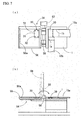
- the producing apparatus 100 of (metal plate)-(ceramic board) laminated assembly of this embodiment is provided with: a mounting table 1 on which the copper-circuit plate 30 on which the temporary-bonding material 72 is plastered is mounted (refer to FIG. 4 ); a base table 2 on which the ceramic board 21 on which the bonding-material layer 71 having a same shape as an outer shape of the copper-circuit plate 30 is formed (refer to FIG.
- a conveying device 3 conveying the copper-circuit plate 30 from the mounting table 1 to the base table 2 and aligning with the ceramic board 21, and laminating the copper-circuit plate 30 and the ceramic board 21 with the bonding-material layer 71 and the temporary-bonding material 72 therebetween; and a heating device 4 provided on a conveying path of the copper-circuit plate 30 by the conveying device 3 so as to melt the temporary-bonding material 72 on the copper-circuit plate 30.
- the producing apparatus 100 is provided with a supplying device 5 arranging the copper-circuit plate 30 on the mounting table 1.
- the supplying device 5 is provided with: a supplying stage 52 moving a tray 51 in which copper-circuit plates 30 are held to a prescribed position in a state in which applied surfaces 31 of the temporary-bonding material 72 are upward; a receiving-pickup cylinder 53 picking pieces of the copper-circuit plates 30 up from the tray 51 on the supplying stage 52; and an inverting device 54 supplying the copper-circuit plates 30 received from the receiving-pickup cylinder 53, in a state in which the applied surfaces 31 of the temporary-bonding material are downward by inverting, onto the mounting table 1.
- the supplying stage 52 is configured to movable between a position in which an operator can mount the tray 51 (a position denoted by the two-dotted chain line) and a position in which the copper-circuit plate 30 can be picked up by the receiving-pickup cylinder 53, so as to convey the tray 51 mounted on the supplying stage 52 by the operator to an operational position of the receiving-pickup cylinder 53.
- an alignment device 55 holding the supplying stage 52 at the position in which the copper-circuit plate 30 can be picked up by the receiving-pickup cylinder 53 is provided.
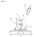
- the receiving-pickup cylinder 53 picks up the copper-circuit plates 30 one by one from the tray 51, and moves them to a turning stage 56 of the inverting device 54, and is held movably along xyz-axes direction by a driving mechanism 6 mentioned below, used for the conveying device 3.
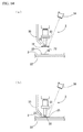
- the inverting device 54 is configured from the turning stage 56 held by a rotary actuator 57 so as to be possible to pivot on a spindle 58 by 180° as shown in FIG. 7 and FIG. 8 .
- a recessed portion 56a is formed to have a smaller depth than the thickness of the copper-circuit plate 30.
- guide walls 1a and 1b which are orthogonally arranged to each other, and pusher portions 15a and 15b which are held movably back and forth toward the guide walls 1a and 1b are provided in order to align the copper-circuit plate 30.
- the copper-circuit plate 30 is positioned at a prescribed position on the mounting table 1.
- the conveying device 3 is configured form a laminating-pickup cylinder 33 provided moveably along xyz-axes direction by the driving mechanism 6.
- the driving mechanism 6 is provided with the movable receiving-pickup cylinder 53 other than the laminating-pickup cylinder 33.
- This conveying device 3 conveys the copper-circuit plate 30 mounted on the mounting table 1 in a state in which the applied surface 31 is downward to the base table 2 on which the ceramic board 21 is mounted in a state in which the applied surface 31 is downward, and laminates the applied surface 31 of the copper-circuit plate 30 on the ceramic board 21 on the base table 2; so that the copper-circuit plate 30 and the ceramic board 21 are laminated.
- the copper-circuit plate 30 is conveyed by air suction of the laminating-pickup cylinder 33 on an upper surface of the copper-circuit plate 30 that is opposite to the applied surface 31.
- the base table 2 is installed on a supplying stage 22 which is movable between a position in which the operator can mount the ceramic board 21 (a position shown by the two-dotted chain line in FIG. 1 ) and a laminating position of the copper-circuit plate 30 (a position shown by the solid line in FIG. 1 ).
- a supplying stage 22 which is movable between a position in which the operator can mount the ceramic board 21 (a position shown by the two-dotted chain line in FIG. 1 ) and a laminating position of the copper-circuit plate 30 (a position shown by the solid line in FIG. 1 ).
- guide pins 23 are stood with intervals around a side surface of the ceramic board 21. Mounting the ceramic board 21 in an area surrounded by the guide pins 23, the ceramic board 21 is positioned on the mounting table 2.
- the heating device 4 melting the temporary-bonding material 72 of the copper-circuit plate 30 is provided.
- the heating device 4 is configured from a rubber heater 41. Arranging the copper-circuit plate 30 so that the applied surface 31 faces the rubber heater 41, the temporary-bonding material 72 on the applied surface 31 is heated and melted.
- the conveying device 3 is provided with a temperature-measuring device 34 which can observe a melted state of the temporary-bonding material 72 while conveying the copper-circuit plate 30. Accordingly, it is possible to confirm melted states of the temporary-bonding material 72 at the time: when the copper-circuit plate 30 is heated by the heating device 4, when the copper-circuit plate 30 is laminated on the ceramic board 21, and after the copper-circuit plate 30 and the ceramic board 21 are laminated each other.
- the temperature-measuring device 34 for example, an infrared thermometer or the like may be used, and it is configured to measure temperature of the copper-circuit plate 30 held by the laminating-pickup cylinder 33 in this embodiment.
- the producing apparatus 100 is provided with a cooling device 35 cooling the copper-circuit plate 30 and the ceramic board 21 after laminating.
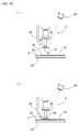
- the cooling device 35 is configured from a cooling nozzle which blows air, as shown in the part (b) of FIG. 10 , and installed at the conveying device 3.
- the bonding-material layer 71 is formed in advance by applying paste of active-metal brazing material.
- the active-metal brazing material is made into a paste by mixing: metal powder including Ag and active metal (e.g., Ti); organic binder such as ethyl cellulose, methyl cellulose, polymethyl methacrylate, acrylic resin, alkyd resin or the like; a solvent such as toluene, cyclohexanone, diacetone alcohol, methyl cellosolve, ethyl cellosolve, terpineol, texanol, triethyl citrate or the like; a dispersing agent, plasticizer, a reducing agent, and the like.
- active metal e.g., Ti
- organic binder such as ethyl cellulose, methyl cellulose, polymethyl methacrylate, acrylic resin, alkyd resin or the like
- solvent such as toluene, cyclohexanone, diacetone alcohol, methyl cell
- the metal powder Ag-8.8 mass% Ti or Ag-27.4 mass% Cu-2.0 mass% Ti may be suitably used.
- this active-metal brazing material applying this active-metal brazing material on positions in which the copper-circuit plates 30 are intended to be bonded at a surface of the ceramic board 21 by screen printing, and then drying it, the bonding-material layer 71 having the same shape pattern as an outer shape of the copper-circuit plate 30 is formed on the surface of the ceramic board 21.
- the active-metal brazing material is turned into porous material when dried. Therefore, the bonding-material layer 71 is porous material having vacant holes.
- the temporary-bonding material 72 including polyethylene glycol (PEG) as major ingredient is applied.
- Polyethylene glycol is solid at normal temperature (25°C), and a phase thereof is transformed to liquid with comparative low melting point.
- Weight-average molecular of 800 to 20000 is suitable for usage. If the weight-average molecular is less than 800, it is liquid at normal temperature, so it is hard to handle. If the weight-average molecular is more than 20000, since melting point is high, applying workability on the copper-circuit plate 30 is poor. If the weight-average molecular is 800 to 1000, the melting point is about 40°C; even though the weight-average molecular is 6000, the melting point is about 60°C.
- the temporary-bonding material 72 By heating and melting the temporary-bonding material 72, and dropping at some positions such as corner portions at the surface of the copper-circuit plate 30, for example, so that the temporary-bonding material 72 is applied on the surface of the copper-circuit plate 30. Then, by cooling to the normal temperature and solidifying the temporary-bonding material 72 dropped on the copper-circuit plate 30, the copper-circuit plate 30 with the temporary-bonding material 72 is made.
- the copper-circuit plates 30 on which the temporary-bonding material 72 is applied are disposed in the recessed portions in the tray 51 in a state in which the temporary-bonding material 72 upward, and conveyed onto the supplying stage 52.
- the temporary-bonding material 72 may be applied on the copper-circuit plate 30 by dropping the temporary-bonding material 72 on the copper-circuit plate 30 disposed in the tray 51.
- the tray 51 is disposed on the supplying stage 52, and then moved to a pickup position for the copper-circuit plate 30 by the receiving-pickup cylinder 53. Then, each of pieces of the copper-circuit plates 30 in the tray 51 is picked up one by one by the receiving-pickup cylinder 53, moved to the turning stage 56, and arranged on the mounting table 1 in a state in which the applied surface 31 of the temporary-bonding material 72 is inverted downward from upward.
- the copper-circuit plate 30 on the mounting table 1 is conveyed by the laminating-pickup cylinder 33 in a state in which the applied surface 31 is downward. While conveying the copper-circuit plate 30 from the mounting table 1 to the base table 2, the applied surface 31 of the copper-circuit plate 30 is faced to the rubber heater 41 so as to be heated. The temporary-bonding material 72 is melted by being heated by the rubber heater 41. At this time, the melting state of the temporary-bonding material 72 can be observed by the temperature-measuring device 34.
- the copper-circuit plate 30 is conveyed to the base table 2 on which the ceramic board 21 is arranged, the applied surface 31 of the copper-circuit plate 30 is laminated on the ceramic board 21.
- the temporary-bonding material 72 adhered on the copper-circuit plate 30 is thinly spread and layered between the copper-circuit plate 30 and the bonding-material layer 71, filled into the vacant holes of the bonding-material layer 71 which is porous material, and bonds them. Since the bonding-material layer 71 and the copper-circuit plate 30 are formed to have the same external shape, these are laminated at accurate position without being misaligned.
- the temporary-bonding material 72 is, as shown in the part (b) of FIG. 10 , solidified by being cooled to normal temperature immediately by the cooling device 35, so that the copper-circuit plate 30 and the ceramic board 21 are held in a positioned state.
- the (metal plate)-(ceramic board) laminated assembly 11 in which the copper-circuit plate 30 and the ceramic board 21 are temporarily tacked with the bonding-material layer 71 therebetween is produced.
- the temporary-bonding material 72 applied on the copper-circuit plate 30 is solidified when conveying, the temporary-bonding material 72 can be melted by heating by the heating device 4 while conveying the copper-circuit plate 30 from the mounting table 1 to the base plate 2. Then, the copper-circuit plate 30 can be laminated on the ceramic board 21 in a state in which the temporary-bonding material 72 is melted.
- the copper-circuit plate 20 is temporarily tacked on the bonding-material layer 71 on the ceramic board 21 by the temporary-bonding material 72, so that the copper-circuit plate 30 and the bonding-material layer 71 on the ceramic board 21 is prevented from being misaligned while bonding operations or the like in the subsequent bonding process; accordingly, the copper-circuit plate 30 can be bonded on the prescribed position of the ceramic board 21 with an accurately positioned state.
- the ceramic board 21 and the copper-circuit plate 30 can be bonded by the bonding-material layer 71 therebetween by heating in vacuum remaining the pressurizing state in the laminating direction.
- the bonding material includes active metal, being heated in vacuum, Ti which is active metal reacts to N or O included in the ceramic board 21 and forms nitride, oxide and the like on the surface of the ceramic plate 21; and Ag forms a melted-metal layer by reacting to Cu of the copper-circuit plate 30: and by cooling and solidifying it, the copper-circuit plate 30 and the ceramic board 21 are bonded with an Ag-Cu eutectic layer therebetween.
- the temporary-bonding material 72 is decomposed and disappeared in an initial stage of this heating.
- the heat-radiation plate 40 is bonded to the ceramic board 21 by bonding material such as Al-Si based brazing material, Al-Ge based brazing material, Al-Cu based brazing material, Al-Mg based brazing material, Al-Mn based brazing material or the like.
- such methods can be adopted like: laminating the heat-radiation plate 40 and the ceramic board 21 with the bonding material (a brazing-material foil) therebetween; or temporarily tacking the bonding material on an aluminum plate for forming the heat-radiation plate 40 by welding or the like, and then punching out it so as to make the heat-radiation plate 40 on which the bonding material is temporarily tacked, and laminating the bonding material side of the heat-radiation plate 40 on the ceramic board 21.
- the producing apparatus 100 of the (metal plate)-(ceramic board) laminated assembly of the present embodiment can also be used.
- the heat-radiation plates 40 each are laminated one by one corresponding to a bonding position of each of the copper-circuit plates 30 on the ceramic board 21 at an opposite surface to the bonding surface for the copper-circuit plate 30. Similar to the above-mentioned bonding process of the copper-circuit plate 30, the bonding material (brazing material) and a part of aluminum in the heat-radiation plate 40 are melted by laminating the laminated assemblies laminating heat-radiation plate 40 and heating them in a vacuum heating furnace in a state of being pressurized in the laminating direction: and then the heat-radiation plate 40 is bonded on the ceramic board 21 by cooling and solidifying.
- the respective power-module substrates 10 in which the copper-circuit plate 30 is bonded on one surface of the ceramic board 20 and the heat-radiation plate 40 is bonded on the opposite surface of the ceramic board 20 are made as shown in FIG. 12 .
- the grooves of the ceramic board 21 may be made before bonding the copper-circuit plates 30.
- the heating device 4 is provided in the conveying path of the copper-circuit plate 30. Therefore, it is possible to laminate the copper-circuit plate 30 and the ceramic board 21 immediately in the state in which the temporary-bonding material 72 is melted, so that the copper-circuit plate 30 and the ceramic board 21 can be reliably bonded together with the bonding-material layer 71 therebetween.
- the (metal plate)-(ceramic board) laminated assembly 11 is subsequently heated so that the ceramic board 21 and the copper-circuit plate 30 are bonded by the bonding material.
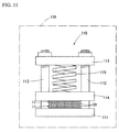
- a pressurizing tool 110 shown in FIG. 11 is used.
- the pressurizing tool 110 is provided with: a base plate 111; guide posts 112 vertically installed at four corners on an upper surface of the base plate 111; a fixed plate 113 fixed on upper parts of the guide posts 112; a pressurizing plate 114 held by the guide posts 112 with being vertically movable between the base plate 111 and the fixed plate 113; and an energizing device 115 such as a spring or the like, arranged between the fixed plate 113 and the pressurizing plate 114, energizing the pressurizing plate 114 downward.
- the (metal plate)-(ceramic board) laminated assemblies 11 are disposed between the base plate 111 and the pressurizing plate 114.
- the (metal plate)-(ceramic board) laminated assemblies 11 are arranged in a heating furnace 120 together with the pressurizing tool 110 in a state in which the pressurizing tool 110 presses the (metal plate)-(ceramic board) laminated assemblies 11, and heated in vacuum at temperature of 800°C or higher and 930°C or lower for 1 minute to 60 minutes; so that the ceramic board 21 and the copper-circuit plate 30 are brazed.
- the bonding device of the present invention is configured from the pressurizing tool 110 and the heating furnace 120 in this embodiment.
- the temporary-bonding material 72 including polyethylene glycol as major ingredient is immediately decomposed before rising up to bonding temperature in the bonding process, so that bonded surfaces are not influenced.
- the copper-circuit plate 30 can be conveyed by the supplying device 5 in the state in which the applied surface 31 of the temporary-bonding material 72 is downward; so that the copper-circuit plate 30 can be arranged on the ceramic board 21 immediately after melting the temporary-bonding material 72.
- the cooling device 35 is provided so as to actively cool the copper-circuit plate 30 and the ceramic board 21 after laminating, it can be immediately made into the state of positioning the copper-circuit plate 30 on the ceramic board 21. Accordingly, it is possible to improve efficiency of the producing process of the power-module substrate 10.
- the temperature-measuring device 34 By the temperature-measuring device 34, the melting state of the temporary-bonding material 72 can be confirmed. Therefore, it is possible to precisely bond the ceramic board 21 and the copper-circuit plate 30 with the bonding-material layer 71 therebetween without poor-quality of temporal-tacking.
- the temperature-measuring device 34 at the conveying device 3 conveying the copper-circuit plate 30, it is possible to confirm the melting state of the temporary-bonding material 72 by the one temperature-measuring device 34 at timings of: heating the copper-circuit plate 30; laminating the copper-circuit plate 30 on the ceramic board 21; and after laminating the copper-circuit plate 30 and the ceramic board 21. Therefore, it is possible to laminate the ceramic board 21 in a state in which the temporary-bonding material 72 is melted altogether; and the (metal plate)-(ceramic board) laminated assembly 11 can be treated in the temporal-tacking state of the copper-circuit plate 30 and the ceramic board 21 after laminating. Accordingly, it is reliably possible to prevent the misalignment of the ceramic board 21 and the copper-circuit plate 30.
- the temporary-bonding material is applied on the copper-circuit plate, and the copper-circuit plate is conveyed and laminated on the ceramic board.
- the ceramic board may be conveyed and laminated on the copper-circuit plate after applying the temporary-bonding material on the bonding-material layer of the ceramic board.
- FIG. 14 shows a process in which the temporary-bonding material 72 is applied on the ceramic board 25 (the bonding-material layer is omitted) and a ceramic board 25 is laminated on the copper-circuit plate 30.
- the ceramic board 25 is illustrated so as to have an area in which a ceramic substrate for a power-module substrate can be formed.
- the ceramic board 25 on which the temporary-bonding material 72 is applied is held by suction by the laminating-pickup cylinder 35, and then conveyed on the base table 2 on which the copper-circuit plate 30 is arranged after heating the temporary-bonding material 72 into a melting state by the heating device (not illustrated), so that the ceramic board 21 is laminated on the copper-circuit plate 30.
- the copper-circuit plate 30 and the ceramic board 25 are fixed by cooling and solidifying the temporary-bonding material 72 by the cooling device 35.
- the ceramic board 25 is the one plate of the present invention
- the copper-circuit plate 30 is the other plate of the present invention.
- the embodiments of cases of producing a power-module substrate in which a copper-circuit plate and a ceramic board are bonded are explained.
- the present invention may be used for a power-module substrate using a metal plate other than a copper-circuit plate (e.g., aluminum, aluminum alloy or the like), for bonding the metal plate and a ceramic board.
- a metal plate other than a copper-circuit plate e.g., aluminum, aluminum alloy or the like
- the present invention is not limited to a power-module substrate: but the present invention can further be used for cases of producing a bonded assembly of a ceramic board and a metal plate for other use than a power module. In those cases, it is applicable to bond these laminated assemblies ((metal plate)-(ceramic board) laminated assemblies) in bonding conditions other than a condition including both pressurizing and heating.
- the temporary-bonding material including polyethylene glycol as major ingredient
- the temporary-bonding material is not limited to this.
- liquid paraffin, wax and the like can be used.
- the bonding-material layer configured from active-metal brazing material is formed on the ceramic board in the embodiments, the bonding-material layer may be formed on the copper-circuit plate. Moreover, the temporary-bonding material may be formed on the bonding-material layer instead of a surface of the ceramic board or the copper-circuit plate.
- the bonding-material layer 71 of the above-described embodiment may be formed by using a foil of active-metal brazing material.
- the present invention enables to prevent a misalignment of the ceramic board, the bonding-material layer, and the metal plate when bonding the metal plate and the ceramic board with the bonding-material layer therebetween, and is applicable suitably for producing a power-module substrate.
Landscapes
- Engineering & Computer Science (AREA)
- Chemical & Material Sciences (AREA)
- Ceramic Engineering (AREA)
- Materials Engineering (AREA)
- Microelectronics & Electronic Packaging (AREA)
- Manufacturing & Machinery (AREA)
- Mechanical Engineering (AREA)
- Structural Engineering (AREA)
- Organic Chemistry (AREA)
- Ceramic Products (AREA)
- Laminated Bodies (AREA)
- Inorganic Chemistry (AREA)
- Manufacturing Of Printed Wiring (AREA)
Applications Claiming Priority (2)
| Application Number | Priority Date | Filing Date | Title |
|---|---|---|---|
| JP2013072421 | 2013-03-29 | ||
| PCT/JP2014/057336 WO2014156835A1 (fr) | 2013-03-29 | 2014-03-18 | Appareil et procédé de production de stratifié (plaque métallique)-(plaque céramique) et appareil et procédé de production de substrat pour des modules de puissance |
Publications (3)
| Publication Number | Publication Date |
|---|---|
| EP2980048A1 true EP2980048A1 (fr) | 2016-02-03 |
| EP2980048A4 EP2980048A4 (fr) | 2016-11-30 |
| EP2980048B1 EP2980048B1 (fr) | 2018-08-08 |
Family
ID=51623815
Family Applications (1)
| Application Number | Title | Priority Date | Filing Date |
|---|---|---|---|
| EP14774133.4A Not-in-force EP2980048B1 (fr) | 2013-03-29 | 2014-03-18 | Appareil et procédé de production d'un assemblage stratifié (plaque métallique)-(plaque céramique) et appareil et procédé de production de substrat pour des modules de puissance |
Country Status (7)
| Country | Link |
|---|---|
| US (1) | US9725367B2 (fr) |
| EP (1) | EP2980048B1 (fr) |
| JP (1) | JP6314567B2 (fr) |
| KR (1) | KR102163533B1 (fr) |
| CN (1) | CN105189409B (fr) |
| TW (2) | TWI608577B (fr) |
| WO (1) | WO2014156835A1 (fr) |
Families Citing this family (11)
| Publication number | Priority date | Publication date | Assignee | Title |
|---|---|---|---|---|
| CN106696475B (zh) * | 2015-11-13 | 2019-06-18 | 富泰华工业(深圳)有限公司 | 打印机及利用打印机打印电路板的方法 |
| JP6700119B2 (ja) * | 2016-06-24 | 2020-05-27 | 三菱電機株式会社 | 電力用半導体装置および電力用半導体装置の製造方法 |
| EP3340287B1 (fr) * | 2016-12-23 | 2020-10-28 | Huawei Technologies Co., Ltd. | Mesure de température basée sur un motif pour un dispositif de collage et un système de collage |
| JP6717245B2 (ja) | 2017-03-17 | 2020-07-01 | 三菱マテリアル株式会社 | 接合体の製造方法、絶縁回路基板の製造方法、及び、ヒートシンク付き絶縁回路基板の製造方法 |
| JP2019009333A (ja) * | 2017-06-27 | 2019-01-17 | 三菱マテリアル株式会社 | セラミックス−金属接合体の製造方法、セラミックス回路基板の製造方法及びセラミックス−金属接合体 |
| JP6939596B2 (ja) * | 2018-01-24 | 2021-09-22 | 三菱マテリアル株式会社 | パワーモジュール用基板の製造方法及びセラミックス‐銅接合体 |
| TWI755906B (zh) * | 2020-10-23 | 2022-02-21 | 尚城科技股份有限公司 | 雙對稱結構交互式影像自動疊板機 |
| CN112312645B (zh) * | 2020-10-28 | 2023-06-02 | 江苏贺鸿智能科技有限公司 | 一种陶瓷散热线路板及其制作方法 |
| WO2023100917A1 (fr) | 2021-11-30 | 2023-06-08 | 三菱マテリアル株式会社 | Pâte métallique pour assemblage, et procédé de fabrication de corps assemblé et procédé de fabrication de carte de circuit imprimé isolée |
| WO2023100939A1 (fr) | 2021-11-30 | 2023-06-08 | 三菱マテリアル株式会社 | Matériau de fixation temporaire, et procédé de fabrication de corps assemblé |
| CN118721414B (zh) * | 2024-06-27 | 2024-12-31 | 湖南旗滨医药材料科技有限公司 | 一种用于制备旋转管的工具及旋转管 |
Family Cites Families (40)
| Publication number | Priority date | Publication date | Assignee | Title |
|---|---|---|---|---|
| US3859399A (en) * | 1971-04-19 | 1975-01-07 | Carborundum Co | Dense composite ceramic bodies and method for their production |
| US4353957A (en) * | 1973-09-24 | 1982-10-12 | Tam Ceramics Inc. | Ceramic matrices for electronic devices and process for forming same |
| DE3204167A1 (de) | 1982-02-06 | 1983-08-11 | Brown, Boveri & Cie Ag, 6800 Mannheim | Verfahren zum direkten verbinden von metallstuecken mit oxidkeramiksubstraten |
| JPH01282285A (ja) * | 1988-05-10 | 1989-11-14 | Tdk Corp | 接着剤による部材相互の接合方法 |
| US4943468A (en) * | 1988-10-31 | 1990-07-24 | Texas Instruments Incorporated | Ceramic based substrate for electronic circuit system modules |
| JPH0394130A (ja) * | 1989-09-06 | 1991-04-18 | Matsushita Electric Ind Co Ltd | リフロー装置 |
| JPH0492485A (ja) * | 1990-08-08 | 1992-03-25 | Mitsubishi Gas Chem Co Inc | 保護箔付きプリント配線材料 |
| JPH0669324A (ja) * | 1992-08-21 | 1994-03-11 | Hitachi Electron Eng Co Ltd | 薄膜部品の仮固定方法 |
| JPH06216499A (ja) * | 1993-01-19 | 1994-08-05 | Toshiba Corp | 銅回路基板の製造方法 |
| JP3185010B2 (ja) * | 1995-01-20 | 2001-07-09 | 同和鉱業株式会社 | 金属−セラミックス複合部材の製造装置 |
| JP4077888B2 (ja) * | 1995-07-21 | 2008-04-23 | 株式会社東芝 | セラミックス回路基板 |
| JPH09153568A (ja) | 1995-09-28 | 1997-06-10 | Toshiba Corp | 窒化珪素セラミック回路基板および半導体装置 |
| JPH09110562A (ja) * | 1995-10-06 | 1997-04-28 | Dowa Mining Co Ltd | 金属−セラミックス複合部材の製造装置 |
| JPH11238961A (ja) | 1998-02-19 | 1999-08-31 | Matsushita Electric Ind Co Ltd | 電子部品の半田付け方法 |
| JP2000036501A (ja) * | 1998-05-12 | 2000-02-02 | Sharp Corp | ダイボンド装置 |
| US6743395B2 (en) * | 2000-03-22 | 2004-06-01 | Ebara Corporation | Composite metallic ultrafine particles and process for producing the same |
| US6799712B1 (en) * | 2001-02-21 | 2004-10-05 | Electronic Controls Design, Inc. | Conveyor oven profiling system |
| US7326274B2 (en) * | 2001-10-18 | 2008-02-05 | Praxis Powder Technology, Inc. | Binder compositions and methods for binder assisted forming |
| US6793120B2 (en) * | 2002-01-17 | 2004-09-21 | Donnelly Corporation | Apparatus and method for mounting an electrical connector to a glass sheet of a vehicle window |
| JP4311303B2 (ja) | 2004-08-17 | 2009-08-12 | 三菱マテリアル株式会社 | パワーモジュール用基板の製造方法 |
| EP1791176B1 (fr) | 2004-08-17 | 2019-07-03 | Mitsubishi Materials Corporation | Procede de fabrication d'un substrat pour module de puissance |
| JP5098165B2 (ja) * | 2005-12-08 | 2012-12-12 | 株式会社ニコン | ウェハの接合方法、接合装置及び積層型半導体装置の製造方法 |
| TWI268189B (en) * | 2006-02-03 | 2006-12-11 | Quanta Comp Inc | Wave solder apparatus |
| CN101971329B (zh) * | 2008-03-17 | 2012-11-21 | 三菱综合材料株式会社 | 带散热片的功率模块用基板及其制造方法、以及带散热片的功率模块、功率模块用基板 |
| US9289142B2 (en) * | 2008-03-24 | 2016-03-22 | Neuronexus Technologies, Inc. | Implantable electrode lead system with a three dimensional arrangement and method of making the same |
| JP5077102B2 (ja) | 2008-06-30 | 2012-11-21 | 三菱マテリアル株式会社 | パワーモジュール用基板及びその製造方法 |
| US8058150B2 (en) * | 2008-07-10 | 2011-11-15 | Taiwan Semiconductor Manufacturing Company, Ltd. | Particle free wafer separation |
| JP2010050164A (ja) | 2008-08-19 | 2010-03-04 | Mitsubishi Materials Corp | パワーモジュール用基板の製造方法 |
| CH700774A1 (de) * | 2009-03-31 | 2010-10-15 | Alstom Technology Ltd | Doppellotelement, Verfahren zu dessen Herstellung und Verwendungen desselben. |
| US8546238B2 (en) * | 2009-04-22 | 2013-10-01 | Commissariat A L'energie Atomique Et Aux Energies | Method for transferring at least one micro-technological layer |
| EP2365949A2 (fr) * | 2009-07-07 | 2011-09-21 | Morgan Advanced Materials And Technology Inc. | Article hybride céramique dure non oxyde ou oxyde/composite de céramique dure non oxyde ou oxyde |
| JP5310634B2 (ja) * | 2010-04-09 | 2013-10-09 | 千住金属工業株式会社 | はんだ付け装置 |
| JP5807221B2 (ja) * | 2010-06-28 | 2015-11-10 | アユミ工業株式会社 | 接合構造体製造方法および加熱溶融処理方法ならびにこれらのシステム |
| BR112013023327A2 (pt) * | 2011-03-11 | 2016-12-13 | Ceramtec Gmbh | corpos de bobinas com núcleo de cerâmica |
| JP5821389B2 (ja) * | 2011-04-20 | 2015-11-24 | 三菱マテリアル株式会社 | パワーモジュール用基板の製造方法及びパワーモジュール用基板 |
| JP6011074B2 (ja) * | 2012-01-20 | 2016-10-19 | 富士通株式会社 | 電子装置の製造方法及び電子装置の製造装置 |
| DE102012103430B4 (de) * | 2012-04-19 | 2015-10-22 | Ev Group E. Thallner Gmbh | Verfahren zum Heften von Chips auf ein Substrat |
| US20160017184A1 (en) * | 2013-03-06 | 2016-01-21 | John Moore | Adhesive with tunable porosity and methods to support temporary bonding applications |
| JP5664679B2 (ja) | 2013-03-07 | 2015-02-04 | 三菱マテリアル株式会社 | パワーモジュール用基板の製造方法 |
| WO2014174854A1 (fr) * | 2013-04-25 | 2014-10-30 | 富士電機株式会社 | Dispositif à semi-conducteur |
-
2014
- 2014-03-18 US US14/780,779 patent/US9725367B2/en not_active Expired - Fee Related
- 2014-03-18 JP JP2014054770A patent/JP6314567B2/ja not_active Expired - Fee Related
- 2014-03-18 EP EP14774133.4A patent/EP2980048B1/fr not_active Not-in-force
- 2014-03-18 WO PCT/JP2014/057336 patent/WO2014156835A1/fr not_active Ceased
- 2014-03-18 KR KR1020157027461A patent/KR102163533B1/ko active Active
- 2014-03-18 CN CN201480013541.6A patent/CN105189409B/zh not_active Expired - Fee Related
- 2014-03-26 TW TW103111243A patent/TWI608577B/zh not_active IP Right Cessation
- 2014-03-26 TW TW106126586A patent/TWI629754B/zh not_active IP Right Cessation
Also Published As
| Publication number | Publication date |
|---|---|
| KR20150139850A (ko) | 2015-12-14 |
| TWI629754B (zh) | 2018-07-11 |
| US20160052830A1 (en) | 2016-02-25 |
| JP2014209591A (ja) | 2014-11-06 |
| US9725367B2 (en) | 2017-08-08 |
| JP6314567B2 (ja) | 2018-04-25 |
| EP2980048B1 (fr) | 2018-08-08 |
| TW201513274A (zh) | 2015-04-01 |
| KR102163533B1 (ko) | 2020-10-08 |
| CN105189409B (zh) | 2018-11-09 |
| TWI608577B (zh) | 2017-12-11 |
| CN105189409A (zh) | 2015-12-23 |
| TW201742198A (zh) | 2017-12-01 |
| WO2014156835A1 (fr) | 2014-10-02 |
| EP2980048A4 (fr) | 2016-11-30 |
Similar Documents
| Publication | Publication Date | Title |
|---|---|---|
| EP2980048B1 (fr) | Appareil et procédé de production d'un assemblage stratifié (plaque métallique)-(plaque céramique) et appareil et procédé de production de substrat pour des modules de puissance | |
| EP2966679B1 (fr) | Procédé de fabrication de substrat de module de puissance | |
| CN106471616B (zh) | 接合体和多层接合体制法、功率模块基板和带散热器功率模块基板制法及层叠体制造装置 | |
| US20190184480A1 (en) | Precise Alignment and Decal Bonding of a Pattern of Solder Preforms to a Surface | |
| JP5146296B2 (ja) | パワーモジュール用基板の製造方法 | |
| JP7814521B2 (ja) | 積層モジュールプリフォームを使用して電気部品及び機械部品を接合する方法 | |
| JP5131205B2 (ja) | パワーモジュール用基板の製造方法 | |
| JP5887907B2 (ja) | パワーモジュール用基板の製造方法および製造装置 | |
| CN107845713A (zh) | 固晶稳固方法 | |
| JP2010183013A (ja) | 回路基板の製造方法 | |
| JP5331022B2 (ja) | 配線基板の製造方法 | |
| JP7615769B2 (ja) | 絶縁回路基板の製造方法 | |
| JP2021118189A (ja) | 金属回路パターンおよび金属回路パターンの製造方法 | |
| JPH1167988A (ja) | 配線基板構造物及び配線基板 | |
| JP2010278236A (ja) | 電子部品の製造方法 | |
| JPH0228393A (ja) | 銅張積層配線板の製造方法 |
Legal Events
| Date | Code | Title | Description |
|---|---|---|---|
| PUAI | Public reference made under article 153(3) epc to a published international application that has entered the european phase |
Free format text: ORIGINAL CODE: 0009012 |
|
| 17P | Request for examination filed |
Effective date: 20151015 |
|
| AK | Designated contracting states |
Kind code of ref document: A1 Designated state(s): AL AT BE BG CH CY CZ DE DK EE ES FI FR GB GR HR HU IE IS IT LI LT LU LV MC MK MT NL NO PL PT RO RS SE SI SK SM TR |
|
| AX | Request for extension of the european patent |
Extension state: BA ME |
|
| DAX | Request for extension of the european patent (deleted) | ||
| A4 | Supplementary search report drawn up and despatched |
Effective date: 20161028 |
|
| RIC1 | Information provided on ipc code assigned before grant |
Ipc: C04B 37/02 20060101AFI20161024BHEP Ipc: H01L 23/12 20060101ALI20161024BHEP Ipc: H05K 3/38 20060101ALI20161024BHEP Ipc: B23K 1/20 20060101ALI20161024BHEP Ipc: H05K 3/34 20060101ALI20161024BHEP |
|
| GRAP | Despatch of communication of intention to grant a patent |
Free format text: ORIGINAL CODE: EPIDOSNIGR1 |
|
| STAA | Information on the status of an ep patent application or granted ep patent |
Free format text: STATUS: GRANT OF PATENT IS INTENDED |
|
| INTG | Intention to grant announced |
Effective date: 20180409 |
|
| GRAS | Grant fee paid |
Free format text: ORIGINAL CODE: EPIDOSNIGR3 |
|
| GRAA | (expected) grant |
Free format text: ORIGINAL CODE: 0009210 |
|
| STAA | Information on the status of an ep patent application or granted ep patent |
Free format text: STATUS: THE PATENT HAS BEEN GRANTED |
|
| AK | Designated contracting states |
Kind code of ref document: B1 Designated state(s): AL AT BE BG CH CY CZ DE DK EE ES FI FR GB GR HR HU IE IS IT LI LT LU LV MC MK MT NL NO PL PT RO RS SE SI SK SM TR |
|
| REG | Reference to a national code |
Ref country code: GB Ref legal event code: FG4D |
|
| REG | Reference to a national code |
Ref country code: CH Ref legal event code: EP Ref country code: AT Ref legal event code: REF Ref document number: 1026778 Country of ref document: AT Kind code of ref document: T Effective date: 20180815 |
|
| REG | Reference to a national code |
Ref country code: IE Ref legal event code: FG4D |
|
| REG | Reference to a national code |
Ref country code: DE Ref legal event code: R096 Ref document number: 602014030067 Country of ref document: DE |
|
| REG | Reference to a national code |
Ref country code: NL Ref legal event code: MP Effective date: 20180808 |
|
| REG | Reference to a national code |
Ref country code: LT Ref legal event code: MG4D |
|
| REG | Reference to a national code |
Ref country code: AT Ref legal event code: MK05 Ref document number: 1026778 Country of ref document: AT Kind code of ref document: T Effective date: 20180808 |
|
| PG25 | Lapsed in a contracting state [announced via postgrant information from national office to epo] |
Ref country code: PL Free format text: LAPSE BECAUSE OF FAILURE TO SUBMIT A TRANSLATION OF THE DESCRIPTION OR TO PAY THE FEE WITHIN THE PRESCRIBED TIME-LIMIT Effective date: 20180808 Ref country code: LT Free format text: LAPSE BECAUSE OF FAILURE TO SUBMIT A TRANSLATION OF THE DESCRIPTION OR TO PAY THE FEE WITHIN THE PRESCRIBED TIME-LIMIT Effective date: 20180808 Ref country code: SE Free format text: LAPSE BECAUSE OF FAILURE TO SUBMIT A TRANSLATION OF THE DESCRIPTION OR TO PAY THE FEE WITHIN THE PRESCRIBED TIME-LIMIT Effective date: 20180808 Ref country code: AT Free format text: LAPSE BECAUSE OF FAILURE TO SUBMIT A TRANSLATION OF THE DESCRIPTION OR TO PAY THE FEE WITHIN THE PRESCRIBED TIME-LIMIT Effective date: 20180808 Ref country code: NO Free format text: LAPSE BECAUSE OF FAILURE TO SUBMIT A TRANSLATION OF THE DESCRIPTION OR TO PAY THE FEE WITHIN THE PRESCRIBED TIME-LIMIT Effective date: 20181108 Ref country code: NL Free format text: LAPSE BECAUSE OF FAILURE TO SUBMIT A TRANSLATION OF THE DESCRIPTION OR TO PAY THE FEE WITHIN THE PRESCRIBED TIME-LIMIT Effective date: 20180808 Ref country code: BG Free format text: LAPSE BECAUSE OF FAILURE TO SUBMIT A TRANSLATION OF THE DESCRIPTION OR TO PAY THE FEE WITHIN THE PRESCRIBED TIME-LIMIT Effective date: 20181108 Ref country code: IS Free format text: LAPSE BECAUSE OF FAILURE TO SUBMIT A TRANSLATION OF THE DESCRIPTION OR TO PAY THE FEE WITHIN THE PRESCRIBED TIME-LIMIT Effective date: 20181208 Ref country code: FI Free format text: LAPSE BECAUSE OF FAILURE TO SUBMIT A TRANSLATION OF THE DESCRIPTION OR TO PAY THE FEE WITHIN THE PRESCRIBED TIME-LIMIT Effective date: 20180808 Ref country code: RS Free format text: LAPSE BECAUSE OF FAILURE TO SUBMIT A TRANSLATION OF THE DESCRIPTION OR TO PAY THE FEE WITHIN THE PRESCRIBED TIME-LIMIT Effective date: 20180808 Ref country code: GR Free format text: LAPSE BECAUSE OF FAILURE TO SUBMIT A TRANSLATION OF THE DESCRIPTION OR TO PAY THE FEE WITHIN THE PRESCRIBED TIME-LIMIT Effective date: 20181109 |
|
| PG25 | Lapsed in a contracting state [announced via postgrant information from national office to epo] |
Ref country code: HR Free format text: LAPSE BECAUSE OF FAILURE TO SUBMIT A TRANSLATION OF THE DESCRIPTION OR TO PAY THE FEE WITHIN THE PRESCRIBED TIME-LIMIT Effective date: 20180808 Ref country code: AL Free format text: LAPSE BECAUSE OF FAILURE TO SUBMIT A TRANSLATION OF THE DESCRIPTION OR TO PAY THE FEE WITHIN THE PRESCRIBED TIME-LIMIT Effective date: 20180808 Ref country code: LV Free format text: LAPSE BECAUSE OF FAILURE TO SUBMIT A TRANSLATION OF THE DESCRIPTION OR TO PAY THE FEE WITHIN THE PRESCRIBED TIME-LIMIT Effective date: 20180808 |
|
| PG25 | Lapsed in a contracting state [announced via postgrant information from national office to epo] |
Ref country code: ES Free format text: LAPSE BECAUSE OF FAILURE TO SUBMIT A TRANSLATION OF THE DESCRIPTION OR TO PAY THE FEE WITHIN THE PRESCRIBED TIME-LIMIT Effective date: 20180808 Ref country code: IT Free format text: LAPSE BECAUSE OF FAILURE TO SUBMIT A TRANSLATION OF THE DESCRIPTION OR TO PAY THE FEE WITHIN THE PRESCRIBED TIME-LIMIT Effective date: 20180808 Ref country code: RO Free format text: LAPSE BECAUSE OF FAILURE TO SUBMIT A TRANSLATION OF THE DESCRIPTION OR TO PAY THE FEE WITHIN THE PRESCRIBED TIME-LIMIT Effective date: 20180808 Ref country code: CZ Free format text: LAPSE BECAUSE OF FAILURE TO SUBMIT A TRANSLATION OF THE DESCRIPTION OR TO PAY THE FEE WITHIN THE PRESCRIBED TIME-LIMIT Effective date: 20180808 |
|
| REG | Reference to a national code |
Ref country code: DE Ref legal event code: R097 Ref document number: 602014030067 Country of ref document: DE |
|
| PG25 | Lapsed in a contracting state [announced via postgrant information from national office to epo] |
Ref country code: SK Free format text: LAPSE BECAUSE OF FAILURE TO SUBMIT A TRANSLATION OF THE DESCRIPTION OR TO PAY THE FEE WITHIN THE PRESCRIBED TIME-LIMIT Effective date: 20180808 Ref country code: SM Free format text: LAPSE BECAUSE OF FAILURE TO SUBMIT A TRANSLATION OF THE DESCRIPTION OR TO PAY THE FEE WITHIN THE PRESCRIBED TIME-LIMIT Effective date: 20180808 Ref country code: DK Free format text: LAPSE BECAUSE OF FAILURE TO SUBMIT A TRANSLATION OF THE DESCRIPTION OR TO PAY THE FEE WITHIN THE PRESCRIBED TIME-LIMIT Effective date: 20180808 |
|
| PLBE | No opposition filed within time limit |
Free format text: ORIGINAL CODE: 0009261 |
|
| STAA | Information on the status of an ep patent application or granted ep patent |
Free format text: STATUS: NO OPPOSITION FILED WITHIN TIME LIMIT |
|
| 26N | No opposition filed |
Effective date: 20190509 |
|
| PG25 | Lapsed in a contracting state [announced via postgrant information from national office to epo] |
Ref country code: EE Free format text: LAPSE BECAUSE OF FAILURE TO SUBMIT A TRANSLATION OF THE DESCRIPTION OR TO PAY THE FEE WITHIN THE PRESCRIBED TIME-LIMIT Effective date: 20180808 Ref country code: SI Free format text: LAPSE BECAUSE OF FAILURE TO SUBMIT A TRANSLATION OF THE DESCRIPTION OR TO PAY THE FEE WITHIN THE PRESCRIBED TIME-LIMIT Effective date: 20180808 |
|
| PG25 | Lapsed in a contracting state [announced via postgrant information from national office to epo] |
Ref country code: MC Free format text: LAPSE BECAUSE OF FAILURE TO SUBMIT A TRANSLATION OF THE DESCRIPTION OR TO PAY THE FEE WITHIN THE PRESCRIBED TIME-LIMIT Effective date: 20180808 |
|
| REG | Reference to a national code |
Ref country code: CH Ref legal event code: PL |
|
| PG25 | Lapsed in a contracting state [announced via postgrant information from national office to epo] |
Ref country code: LU Free format text: LAPSE BECAUSE OF NON-PAYMENT OF DUE FEES Effective date: 20190318 |
|
| REG | Reference to a national code |
Ref country code: BE Ref legal event code: MM Effective date: 20190331 |
|
| PG25 | Lapsed in a contracting state [announced via postgrant information from national office to epo] |
Ref country code: LI Free format text: LAPSE BECAUSE OF NON-PAYMENT OF DUE FEES Effective date: 20190331 Ref country code: CH Free format text: LAPSE BECAUSE OF NON-PAYMENT OF DUE FEES Effective date: 20190331 Ref country code: IE Free format text: LAPSE BECAUSE OF NON-PAYMENT OF DUE FEES Effective date: 20190318 |
|
| PG25 | Lapsed in a contracting state [announced via postgrant information from national office to epo] |
Ref country code: BE Free format text: LAPSE BECAUSE OF NON-PAYMENT OF DUE FEES Effective date: 20190331 |
|
| PG25 | Lapsed in a contracting state [announced via postgrant information from national office to epo] |
Ref country code: TR Free format text: LAPSE BECAUSE OF FAILURE TO SUBMIT A TRANSLATION OF THE DESCRIPTION OR TO PAY THE FEE WITHIN THE PRESCRIBED TIME-LIMIT Effective date: 20180808 |
|
| PG25 | Lapsed in a contracting state [announced via postgrant information from national office to epo] |
Ref country code: MT Free format text: LAPSE BECAUSE OF NON-PAYMENT OF DUE FEES Effective date: 20190318 Ref country code: PT Free format text: LAPSE BECAUSE OF FAILURE TO SUBMIT A TRANSLATION OF THE DESCRIPTION OR TO PAY THE FEE WITHIN THE PRESCRIBED TIME-LIMIT Effective date: 20181208 |
|
| PG25 | Lapsed in a contracting state [announced via postgrant information from national office to epo] |
Ref country code: CY Free format text: LAPSE BECAUSE OF FAILURE TO SUBMIT A TRANSLATION OF THE DESCRIPTION OR TO PAY THE FEE WITHIN THE PRESCRIBED TIME-LIMIT Effective date: 20180808 |
|
| PG25 | Lapsed in a contracting state [announced via postgrant information from national office to epo] |
Ref country code: HU Free format text: LAPSE BECAUSE OF FAILURE TO SUBMIT A TRANSLATION OF THE DESCRIPTION OR TO PAY THE FEE WITHIN THE PRESCRIBED TIME-LIMIT; INVALID AB INITIO Effective date: 20140318 |
|
| PG25 | Lapsed in a contracting state [announced via postgrant information from national office to epo] |
Ref country code: MK Free format text: LAPSE BECAUSE OF FAILURE TO SUBMIT A TRANSLATION OF THE DESCRIPTION OR TO PAY THE FEE WITHIN THE PRESCRIBED TIME-LIMIT Effective date: 20180808 |
|
| PGFP | Annual fee paid to national office [announced via postgrant information from national office to epo] |
Ref country code: DE Payment date: 20240320 Year of fee payment: 11 Ref country code: GB Payment date: 20240320 Year of fee payment: 11 |
|
| PGFP | Annual fee paid to national office [announced via postgrant information from national office to epo] |
Ref country code: FR Payment date: 20240328 Year of fee payment: 11 |
|
| REG | Reference to a national code |
Ref country code: DE Ref legal event code: R119 Ref document number: 602014030067 Country of ref document: DE |
|
| GBPC | Gb: european patent ceased through non-payment of renewal fee |
Effective date: 20250318 |
|
| PG25 | Lapsed in a contracting state [announced via postgrant information from national office to epo] |
Ref country code: DE Free format text: LAPSE BECAUSE OF NON-PAYMENT OF DUE FEES Effective date: 20251001 |
|
| PG25 | Lapsed in a contracting state [announced via postgrant information from national office to epo] |
Ref country code: GB Free format text: LAPSE BECAUSE OF NON-PAYMENT OF DUE FEES Effective date: 20250318 |
|
| PG25 | Lapsed in a contracting state [announced via postgrant information from national office to epo] |
Ref country code: FR Free format text: LAPSE BECAUSE OF NON-PAYMENT OF DUE FEES Effective date: 20250331 |