EP2996148B1 - Fotodiodenanordnung - Google Patents
Fotodiodenanordnung Download PDFInfo
- Publication number
- EP2996148B1 EP2996148B1 EP15192319.0A EP15192319A EP2996148B1 EP 2996148 B1 EP2996148 B1 EP 2996148B1 EP 15192319 A EP15192319 A EP 15192319A EP 2996148 B1 EP2996148 B1 EP 2996148B1
- Authority
- EP
- European Patent Office
- Prior art keywords
- photodiode array
- hole
- holes
- view
- conduction type
- Prior art date
- Legal status (The legal status is an assumption and is not a legal conclusion. Google has not performed a legal analysis and makes no representation as to the accuracy of the status listed.)
- Expired - Lifetime
Links
Images






Classifications
-
- H—ELECTRICITY
- H10—SEMICONDUCTOR DEVICES; ELECTRIC SOLID-STATE DEVICES NOT OTHERWISE PROVIDED FOR
- H10F—INORGANIC SEMICONDUCTOR DEVICES SENSITIVE TO INFRARED RADIATION, LIGHT, ELECTROMAGNETIC RADIATION OF SHORTER WAVELENGTH OR CORPUSCULAR RADIATION
- H10F99/00—Subject matter not provided for in other groups of this subclass
-
- H—ELECTRICITY
- H10—SEMICONDUCTOR DEVICES; ELECTRIC SOLID-STATE DEVICES NOT OTHERWISE PROVIDED FOR
- H10F—INORGANIC SEMICONDUCTOR DEVICES SENSITIVE TO INFRARED RADIATION, LIGHT, ELECTROMAGNETIC RADIATION OF SHORTER WAVELENGTH OR CORPUSCULAR RADIATION
- H10F39/00—Integrated devices, or assemblies of multiple devices, comprising at least one element covered by group H10F30/00, e.g. radiation detectors comprising photodiode arrays
- H10F39/011—Manufacture or treatment of image sensors covered by group H10F39/12
-
- H—ELECTRICITY
- H10—SEMICONDUCTOR DEVICES; ELECTRIC SOLID-STATE DEVICES NOT OTHERWISE PROVIDED FOR
- H10F—INORGANIC SEMICONDUCTOR DEVICES SENSITIVE TO INFRARED RADIATION, LIGHT, ELECTROMAGNETIC RADIATION OF SHORTER WAVELENGTH OR CORPUSCULAR RADIATION
- H10F39/00—Integrated devices, or assemblies of multiple devices, comprising at least one element covered by group H10F30/00, e.g. radiation detectors comprising photodiode arrays
- H10F39/10—Integrated devices
- H10F39/107—Integrated devices having multiple elements covered by H10F30/00 in a repetitive configuration, e.g. radiation detectors comprising photodiode arrays
-
- H—ELECTRICITY
- H10—SEMICONDUCTOR DEVICES; ELECTRIC SOLID-STATE DEVICES NOT OTHERWISE PROVIDED FOR
- H10F—INORGANIC SEMICONDUCTOR DEVICES SENSITIVE TO INFRARED RADIATION, LIGHT, ELECTROMAGNETIC RADIATION OF SHORTER WAVELENGTH OR CORPUSCULAR RADIATION
- H10F39/00—Integrated devices, or assemblies of multiple devices, comprising at least one element covered by group H10F30/00, e.g. radiation detectors comprising photodiode arrays
- H10F39/10—Integrated devices
- H10F39/12—Image sensors
- H10F39/18—Complementary metal-oxide-semiconductor [CMOS] image sensors; Photodiode array image sensors
-
- H—ELECTRICITY
- H10—SEMICONDUCTOR DEVICES; ELECTRIC SOLID-STATE DEVICES NOT OTHERWISE PROVIDED FOR
- H10F—INORGANIC SEMICONDUCTOR DEVICES SENSITIVE TO INFRARED RADIATION, LIGHT, ELECTROMAGNETIC RADIATION OF SHORTER WAVELENGTH OR CORPUSCULAR RADIATION
- H10F39/00—Integrated devices, or assemblies of multiple devices, comprising at least one element covered by group H10F30/00, e.g. radiation detectors comprising photodiode arrays
- H10F39/10—Integrated devices
- H10F39/12—Image sensors
- H10F39/18—Complementary metal-oxide-semiconductor [CMOS] image sensors; Photodiode array image sensors
- H10F39/189—X-ray, gamma-ray or corpuscular radiation imagers
-
- H—ELECTRICITY
- H10—SEMICONDUCTOR DEVICES; ELECTRIC SOLID-STATE DEVICES NOT OTHERWISE PROVIDED FOR
- H10F—INORGANIC SEMICONDUCTOR DEVICES SENSITIVE TO INFRARED RADIATION, LIGHT, ELECTROMAGNETIC RADIATION OF SHORTER WAVELENGTH OR CORPUSCULAR RADIATION
- H10F39/00—Integrated devices, or assemblies of multiple devices, comprising at least one element covered by group H10F30/00, e.g. radiation detectors comprising photodiode arrays
- H10F39/80—Constructional details of image sensors
- H10F39/811—Interconnections
-
- H—ELECTRICITY
- H10—SEMICONDUCTOR DEVICES; ELECTRIC SOLID-STATE DEVICES NOT OTHERWISE PROVIDED FOR
- H10W—GENERIC PACKAGES, INTERCONNECTIONS, CONNECTORS OR OTHER CONSTRUCTIONAL DETAILS OF DEVICES COVERED BY CLASS H10
- H10W20/00—Interconnections in chips, wafers or substrates
- H10W20/01—Manufacture or treatment
- H10W20/021—Manufacture or treatment of interconnections within wafers or substrates
- H10W20/023—Manufacture or treatment of interconnections within wafers or substrates the interconnections being through-semiconductor vias
-
- H—ELECTRICITY
- H10—SEMICONDUCTOR DEVICES; ELECTRIC SOLID-STATE DEVICES NOT OTHERWISE PROVIDED FOR
- H10W—GENERIC PACKAGES, INTERCONNECTIONS, CONNECTORS OR OTHER CONSTRUCTIONAL DETAILS OF DEVICES COVERED BY CLASS H10
- H10W20/00—Interconnections in chips, wafers or substrates
- H10W20/01—Manufacture or treatment
- H10W20/021—Manufacture or treatment of interconnections within wafers or substrates
- H10W20/023—Manufacture or treatment of interconnections within wafers or substrates the interconnections being through-semiconductor vias
- H10W20/0242—Manufacture or treatment of interconnections within wafers or substrates the interconnections being through-semiconductor vias comprising etching via holes from the back sides of the chips, wafers or substrates
-
- H—ELECTRICITY
- H10—SEMICONDUCTOR DEVICES; ELECTRIC SOLID-STATE DEVICES NOT OTHERWISE PROVIDED FOR
- H10W—GENERIC PACKAGES, INTERCONNECTIONS, CONNECTORS OR OTHER CONSTRUCTIONAL DETAILS OF DEVICES COVERED BY CLASS H10
- H10W20/00—Interconnections in chips, wafers or substrates
- H10W20/01—Manufacture or treatment
- H10W20/021—Manufacture or treatment of interconnections within wafers or substrates
- H10W20/023—Manufacture or treatment of interconnections within wafers or substrates the interconnections being through-semiconductor vias
- H10W20/0245—Manufacture or treatment of interconnections within wafers or substrates the interconnections being through-semiconductor vias comprising use of blind vias during the manufacture
-
- H—ELECTRICITY
- H10—SEMICONDUCTOR DEVICES; ELECTRIC SOLID-STATE DEVICES NOT OTHERWISE PROVIDED FOR
- H10W—GENERIC PACKAGES, INTERCONNECTIONS, CONNECTORS OR OTHER CONSTRUCTIONAL DETAILS OF DEVICES COVERED BY CLASS H10
- H10W20/00—Interconnections in chips, wafers or substrates
- H10W20/20—Interconnections within wafers or substrates, e.g. through-silicon vias [TSV]
-
- H—ELECTRICITY
- H10—SEMICONDUCTOR DEVICES; ELECTRIC SOLID-STATE DEVICES NOT OTHERWISE PROVIDED FOR
- H10W—GENERIC PACKAGES, INTERCONNECTIONS, CONNECTORS OR OTHER CONSTRUCTIONAL DETAILS OF DEVICES COVERED BY CLASS H10
- H10W20/00—Interconnections in chips, wafers or substrates
- H10W20/20—Interconnections within wafers or substrates, e.g. through-silicon vias [TSV]
- H10W20/211—Through-semiconductor vias, e.g. TSVs
- H10W20/212—Top-view shapes or dispositions, e.g. top-view layouts of the vias
- H10W20/2125—Top-view shapes
-
- H—ELECTRICITY
- H10—SEMICONDUCTOR DEVICES; ELECTRIC SOLID-STATE DEVICES NOT OTHERWISE PROVIDED FOR
- H10W—GENERIC PACKAGES, INTERCONNECTIONS, CONNECTORS OR OTHER CONSTRUCTIONAL DETAILS OF DEVICES COVERED BY CLASS H10
- H10W20/00—Interconnections in chips, wafers or substrates
- H10W20/20—Interconnections within wafers or substrates, e.g. through-silicon vias [TSV]
- H10W20/211—Through-semiconductor vias, e.g. TSVs
- H10W20/216—Through-semiconductor vias, e.g. TSVs characterised by dielectric material at least partially filling the via holes, e.g. covering the through-semiconductor vias in the via holes
-
- H—ELECTRICITY
- H10—SEMICONDUCTOR DEVICES; ELECTRIC SOLID-STATE DEVICES NOT OTHERWISE PROVIDED FOR
- H10W—GENERIC PACKAGES, INTERCONNECTIONS, CONNECTORS OR OTHER CONSTRUCTIONAL DETAILS OF DEVICES COVERED BY CLASS H10
- H10W72/00—Interconnections or connectors in packages
- H10W72/20—Bump connectors, e.g. solder bumps or copper pillars; Dummy bumps; Thermal bumps
- H10W72/241—Dispositions, e.g. layouts
- H10W72/242—Dispositions, e.g. layouts relative to the surface, e.g. recessed, protruding
-
- H—ELECTRICITY
- H10—SEMICONDUCTOR DEVICES; ELECTRIC SOLID-STATE DEVICES NOT OTHERWISE PROVIDED FOR
- H10W—GENERIC PACKAGES, INTERCONNECTIONS, CONNECTORS OR OTHER CONSTRUCTIONAL DETAILS OF DEVICES COVERED BY CLASS H10
- H10W72/00—Interconnections or connectors in packages
- H10W72/20—Bump connectors, e.g. solder bumps or copper pillars; Dummy bumps; Thermal bumps
- H10W72/251—Materials
- H10W72/252—Materials comprising solid metals or solid metalloids, e.g. PbSn, Ag or Cu
-
- H—ELECTRICITY
- H10—SEMICONDUCTOR DEVICES; ELECTRIC SOLID-STATE DEVICES NOT OTHERWISE PROVIDED FOR
- H10W—GENERIC PACKAGES, INTERCONNECTIONS, CONNECTORS OR OTHER CONSTRUCTIONAL DETAILS OF DEVICES COVERED BY CLASS H10
- H10W72/00—Interconnections or connectors in packages
- H10W72/20—Bump connectors, e.g. solder bumps or copper pillars; Dummy bumps; Thermal bumps
- H10W72/29—Bond pads specially adapted therefor
-
- H—ELECTRICITY
- H10—SEMICONDUCTOR DEVICES; ELECTRIC SOLID-STATE DEVICES NOT OTHERWISE PROVIDED FOR
- H10W—GENERIC PACKAGES, INTERCONNECTIONS, CONNECTORS OR OTHER CONSTRUCTIONAL DETAILS OF DEVICES COVERED BY CLASS H10
- H10W72/00—Interconnections or connectors in packages
- H10W72/90—Bond pads, in general
-
- H—ELECTRICITY
- H10—SEMICONDUCTOR DEVICES; ELECTRIC SOLID-STATE DEVICES NOT OTHERWISE PROVIDED FOR
- H10W—GENERIC PACKAGES, INTERCONNECTIONS, CONNECTORS OR OTHER CONSTRUCTIONAL DETAILS OF DEVICES COVERED BY CLASS H10
- H10W72/00—Interconnections or connectors in packages
- H10W72/90—Bond pads, in general
- H10W72/941—Dispositions of bond pads
- H10W72/942—Dispositions of bond pads relative to underlying supporting features, e.g. bond pads, RDLs or vias
Definitions
- the present invention relates to a photodiode array.
- An increase in area has been demanded for a CT (computed tomography) diode array.
- CT computed tomography
- three-dimensional mounting for disposing a signal processing part on the side (back side) opposite the light incidence surface is required.
- electrodes formed on the incidence surface side (front surface side) are extended to the opposite side (back side) of the incidence surface by using through-hole interconnections.
- Patent Document 1 Semiconductor devices using such through-hole interconnections are disclosed in, for example, Patent Document 1, Patent Document 2 and Patent Document 3, etc., described below.
- a substrate is etched by using wet etching using an alkali solution to form through-holes, so that the substrate is etched at an angle of 54.7 degrees with respect to the substrate front surface.
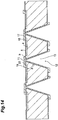
- FIG 14 is a sectional view of a photodiode array of a prior art.
- an object of the invention is to solve the above-mentioned problem and provide a photodiode array in which conducting errors hardly occur in the through-hole interconnections and has a high aperture ratio.
- JP-A-2002 237468 shows an image sensor having a photo-electric conversion element area.
- the disclosed device has a semiconductor structure with an N-type substrate containing a through hole. A high impurity concentration layer of P-type is formed through the through hole, under an oxide film.
- the present invention provides a photodiode array for a computed tomography in accordance with claim 1.
- FIG. 1 is a plan view of a part of a photodiode array of a first embodiment of the invention in an enlarged manner
- FIG. 2 is a sectional view of the same.
- the photodiode array 1 of this embodiment includes a plurality of pn junctions (photodiodes) 4 arranged in an orderly array form longitudinally and laterally on the front surface side, and each of the pn junctions has a function as a photosensitive pixel.
- the photodiode array 1 has an n-type silicon substrate 3 with a thickness of 270 ⁇ m and an impurity concentration of 1 ⁇ 10 12 to 10 15 /cm 3 , and a plurality of p-type impurity diffused layers 5 with a size of 500 ⁇ m ⁇ 500 ⁇ m and an impurity concentration of 1 ⁇ 10 13 to 10 20 /cm 3 are arranged at pitches of approximately 1.5mm.
- the photosensitive pixels are formed by pn junctions 4 formed of the n-type silicon substrate 3 and the plurality of p-type impurity diffused layers 5. Between the p-type impurity diffused layers 5, n + -type impurity regions (separation layers) 7 that separate the photodiodes and reduce dark currents by trapping unnecessary carriers are arranged. On the back side, n + side electrodes 21 are formed.
- a first hole portion 11 perpendicular hole portion
- a second hole portion 13 (pyramidal hole portion) is formed on the back side.
- FIG 3A is a plan view of a portion where a through-hole is formed
- FIG 3B is a III-III arrow longitudinal sectional view of the portion where a through-hole is formed
- FIG 3C is a perspective view of the portion where a through-hole is formed.
- the through-hole 12 is formed by connecting the first hole portion 11 and the second hole portion 13.
- the first hole portion 11 is opened at a diameter of 10 ⁇ m on the front side of the substrate, in parallel to the thickness direction of the substrate.
- the first hole portion 11 is formed into a columnar shape in parallel to the thickness direction of the substrate at a position penetrating the separation layer 7.
- the depth of the hole is formed to be equal to or deeper than the depth of the p-type impurity diffused layer.
- the second hole portion 13 does not limit the depletion layer extending from the pn junction 4, whereby the p-type impurity diffused layers 5 can be provided proximate to each other.
- the second hole portion 13 is formed into a quadrangular pyramidal shape from the substrate back side, and its hole diameter increases toward the back side and becomes smaller toward the front side. Since the second hole portion 13 is formed from the back side by anisotropic etching, the (111) plane is exposed to the hole portion wall face, and the wall face has an angle of approximately 54.7 degrees with respect to the front surface of the photodiode array ( ⁇ :the angle of FIG 3B ⁇ 54.7 degrees). By forming the second hole portion 13 into a quadrangular pyramid, it becomes easy to provide a conductor layer (through-hole interconnection) on the hole portion inner wall.
- the through-hole interconnection 17 is formed from aluminum on the upper layer of the thermal oxide film 9, and is in contact with the p-type impurity diffused layer 5 through the contact hole 15 opened through the thermal oxide film 9. Furthermore, it is formed continuously to the back side through the wall face of the through-hole 12, and can make electrical contact with the p-type impurity diffused layer 5 from the back side. In this case, even when the first hole portion 11 is filled with the metal of the through-hole interconnection 17 and spatially isolates the substrate front side and the substrate back side from each other, there is no problem since the electrical contact between the p-type impurity diffused layer 5 and the back side is not lost (see FIG 4 ).
- FIG 4 is a sectional view of a photodiode array.
- the inside of the first hole portion 11 is filled with the through-hole interconnection 17, however, the back surface of the photodiode array is electrically connected to the p-type impurity diffused layer 5.
- the material of the through-hole interconnection 17 is not limited to aluminum, and copper, nickel, gold, tungsten, titanium, or polysilicon, etc., or an alloy or laminated metal containing these may be used.
- an oxide film obtained by CVD may be used instead of the thermal oxide film 9.
- An oxide film or nitride film obtained by CVD may interpose between the thermal oxide film 9 and the through-hole interconnection 17. Thereby, high insulation performance can be obtained between the silicon substrate and the through-hole interconnection 17.
- FIG 5 is a sectional view of a photodiode array.
- a filling material 10 such as a resin or the like in the upper layer of the through-hole interconnection 17 inside the through-hole 12
- thethrough-hole is filled up.
- the substrate front side and the back side are spatially isolated from each other, however, the electrical contact between the p-type impurity diffused layers 5 and the back side is not lost, and the mechanical strength of the photodiode array 1 can be improved.
- a resin-based insulating material containing epoxy, polyimide, acryl, silicone, and urethane, etc., or an electrical conductive resin containing an electrical conductive filler in these insulating materials is used as a material to be filled in the through-hole 12.
- FIG 6 is a sectional view of a photodiode array.
- the through-hole 12 may be filled up by filling the conductive material 10 inside the through-hole 12.
- the filled conductive material not only improves the mechanical strength of the photodiode array 1 but also is used as a bump electrode by protruding it over the edge of the back surface of the second hole portion 13 and forming the portion protruding over the back surface edge into a semisphere.
- the conductive material 10 an electrical conductive resin or the like containing solder or an electrical conductive filler is used.
- FIG 7 is a sectional view of the photodiode array for describing photodiode array manufacturing processes.
- an n-type semiconductor substrate 3 of a crystal (100) plane is prepared.
- a thermal oxide film 9 is formed on the substrate front surface and used as a mask for n + thermal diffusion of the next step.
- the thermal oxide film is opened by a photo-etching process at the positions for separation layers 7 and phosphorus is thermally diffused and thermal oxidization is applied. At this point, phosphorus is also diffused all over the back surface, and an n + -type impurity concentration layer 19 is formed.
- FIG 8 is a sectional view of the photodiode array for describing photodiode array manufacturing processes.
- a silicon nitride film (SiN x ) 23 is formed by plasma CVD or LP-CVD on the back surface (see FIG. 8 ), and the silicon nitride film 23 and the thermal oxide film 9 at the portions for forming the second hole portions 13 are removed by etching.
- the portions for forming the second hole portions 13 are at positions on the back side corresponding to the separation layers 7.
- the shape and size of the portions removed of the silicon nitride film 23 are designed in advance so that the apexes of the quadrangular pyramids of the second hole portions 13 do not reach the substrate front side by alkali etching described later and the apexes of the quadrangular pyramids are at positions corresponding to the separation layers 7 on the front side.
- FIG 9 is a sectional view of the photodiode array for describing photodiode array manufacturing processes.
- anisotropic etching is applied to the semiconductor substrate 3 from the back side by means of alkali (for example, potassium hydroxide, TMAH, hydrazine, EDP, etc) etching to form the second hole portions 13.
- alkali for example, potassium hydroxide, TMAH, hydrazine, EDP, etc
- etching is applied from the crystal (100) plane of the substrate to expose the (111) plane.
- the second hole portions 13 are formed into quadrangular pyramidal shapes by etching, and etching is automatically stopped when etching reaches the apexes of the quadrangular pyramid shapes (see FIG. 9 ).
- etching may be stopped before reaching the apexes of the quadrangular pyramids.
- the portions corresponding to the apexes of formed quadrangular pyramids are dry-etched from the front side and etching is applied until the first hole portions 11 are formed and connected to the quadrangular pyramidal apexes of the second hole portions 13, and through-holes 12 are formed by the first hole portions 11 and the second hole portions 12.
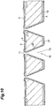
- FIG 10 is a sectional view of the photodiode array for describing photodiode array manufacturing processes.
- n + layers 25 surrounding the through-holes 12 are formed.
- the n + layers 25 are connected to the separation layers 7 and the n + type impurity concentration layers 19 on the back side.
- SiO 2 films 27 are formed by thermal oxidization (see FIG 10 ). Instead of these SiO 2 films 27, the insulating films on the side walls may be laminated films of SiN x or SiO 2 films formed by CVD.
- through-hole interconnections 17 aluminum is deposited from both sides by a sputtering device to form through-hole interconnections 17 and a resist is formed and etching is applied to form a desired pattern.
- the material of the through-hole interconnections 17 is not limited to aluminum, and the method of forming the interconnections is not limited to sputtering.
- diffusion for reducing the electrical resistance may be applied to polysilicon formed by CVD. In this case, only the contact hole portions are made of aluminum and electrically connected to the polysilicon.
- FIG 11 is a sectional view of the photodiode array for describing photodiode array manufacturing processes.
- a photosensitive polyimide layer 29 is formed on the back side, and only portions where bump electrodes 33 are to be arranged are opened. At the same time, portions of the n + side electrodes 21 are also opened and bump electrodes 33 are provided therein. Then, bump electrodes 33 are formed via Under Bump Metal (hereinafter, referred to as UBM) 37 formed from metal that is excellent in electrical and physical connection to the bump electrodes 33.
- UBM Under Bump Metal
- the UBM in this case can be realized by forming Ni-Au by electroless plating or forming Ti-Pt-Au or Cr-Au by the liftoff technology.
- solder bumps can be formed by forming solders on predetermined UBM portions by the solder ball mounting method or printing method and by reflow soldering.
- the bump electrodes 33 are not limited to solder bumps, and may be conductive bumps containing metals such as gold bumps, nickel bumps, copper bumps, or conductive resin bumps.
- FIG 12 is a sectional view of the photodiode array.
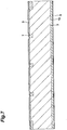
- an n-type semiconductor substrate is prepared and n + -type impurity concentration layers are formed by thermal diffusion, however, as shown in FIG 12 , it is also possible that an n-type semiconductor substrate provided with an n + -type impurity concentration layer by means of thermal diffusion or epitaxial growth in advance is prepared.
- the n + -type impurity concentration layers of the photodiode array can be made thick, and the intervals of the actual p-type impurity diffused layers 5 and the n + -type impurity concentration layers 19 can be narrowed, whereby the resistance components can be reduced and the highspeed response can be improved.
- the second hole portions 13 are formed first from the back side by means of alkali etching, and then the first hole portions 11 are formed, whereby the through-holes 12 are formed. Therefore, at the point of the alkali etching step, the through-holes are not completed yet, so that corrosion to the front side by the alkali etching does not occur, and particularly, there is no harmful influence on the photosensitive surface, so that yield lowering can be prevented.
- etching of the second hole portions 13 stops when it reaches the apexes of the quadrangular pyramidal shapes, so that separate provision of etching stop layers becomes unnecessary. Furthermore, most of the through-holes 12 (second hole portions 13) are formed by anisotropic etching, so that their wall faces have little unevennesses, and smooth through-hole wall faces can be obtained. Therefore, occurrence of unnecessary carriers due to damages on the through-hole wall faces is reduced, resulting in reduction in dark currents.
- FIG 13A and FIG. 13B are sectional views of the portion of the through-hole of the photodiode array.
- the wall face of the second hole portion 13 has an angle of 54.7 degrees with respect to the front surface of the photodiode array, and the wall face of the first hole portion 11 is almost perpendicular to the array direction.
- the through-hole is formed of only the second hole portion 13 by using only alkali etching, the second hole portion and the photodiode array are directly connected, and the angle ⁇ formed between these surfaces is acute.
- the angle B formed at the connecting portion of the hole portions is 90 degrees or more. Furthermore, the angle A between the second hole portion 13 and the photodiode array back surface is also 90 degrees or more, and the angle C between the first hole portion 11 and the photodiode array front surface is almost 90 degrees.
- the through-hole interconnections 17 continued from the front surface to the wall faces of the through-holes 12 and the back surface have no acute angle bends, and conducting failures due to defective coverage caused at the time of forming can be prevented. Furthermore, depending on the dry-etching conditions for forming the first hole portions 11, as shown in FIG. 13B , it is also possible that the first hole portions 11 are tapered and the angle C is formed to be 90 degrees or more. Thereby, conducting failures can be further prevented.
- the second hole portions 13 are formed by alkali etching, so that ion implantation to the wall faces of the through-holes 12 becomes possible, and the n + layers 25 can be easily formed by ion implantation.
- the formed n + layers 25 serve as separation layers separating photodiodes from each other, and performs the function for reducing dark currents by trapping unnecessary carriers.
- the first hole portions 11 are formed so as to penetrate the separation layers 7. Therefore, during dry-etching for forming the first hole portions 11, even if the hole portion inner walls are damaged, generated unnecessary carriers are trapped in the separation layers 7. Therefore, the photodiode array can prevent leak currents caused by damage in the case of forming through-hole interconnections.
- a photodiode array which includes through-hole interconnections that hardly cause conducting failures and has a high aperture ratio can be provided.
- the invention is applicable to a photodiode array.
Landscapes
- Solid State Image Pick-Up Elements (AREA)
- Light Receiving Elements (AREA)
- Photometry And Measurement Of Optical Pulse Characteristics (AREA)
- Internal Circuitry In Semiconductor Integrated Circuit Devices (AREA)
Claims (6)
- Fotodiodenanordnung (1) für eine Computertomographie, umfassend ein Halbleitersubstrat (3) eines ersten Leitungstyps, wobei die Fotodiodenanordnung (1) Folgendes aufweist:eine Vielzahl von Fotodioden (4) vom pn-Übergangstyp, die in einer Anordnung auf einer Lichteinfallsseite des Halbleitersubstrats (3) vom ersten Leitungstyp ausgebildet sind;eine oder mehrere Durchgangsbohrungen (12), die sich jeweils von einer der Lichteinfallsfläche gegenüberliegenden Oberfläche zu der Lichteinfallsfläche durch das Halbleitersubstrat (3) des ersten Leitungstyps erstrecken;einen Isolator (9), der die Wandflächen der einen oder der mehreren Durchgangsbohrungen (12) abdeckt;eine erste leitfähige hochreine Konzentrationsschicht (7) zum Umgeben der einen oder mehreren Durchgangsbohrungen (12), wobei die erste leitfähige hochreine Konzentrationsschicht (7) eine Trennschicht ist, die die Fotodioden (4) trennt; undeine Leiterschicht (17), die auf dem Isolator (9) in den einen oder den mehreren Durchgangsbohrungen (12) ausgebildet ist, die sich von der Einfallsfläche bis zur gegenüberliegenden Oberfläche erstrecken.
- Fotodiodenanordnung (1) nach Anspruch 1, wobei sich die eine oder die mehreren Durchgangsbohrungen (12) von der gegenüberliegenden Oberfläche nach innen in Richtung der Lichteinfallsfläche verjüngen.
- Fotodiodenanordnung (1) nach Anspruch 1, ferner umfassend ein Füllmaterial (10) aus Harz, das die eine oder mehrere Durchgangsbohrungen (12) füllt.
- Fotodiodenanordnung (1) nach Anspruch 1, ferner umfassend ein leitfähiges Material (10), das die eine oder die mehreren Durchgangsbohrungen (12) füllt.
- Fotodiodenanordnung (1) nach einem der Ansprüche 1 bis 3, wobei die Tiefe der ersten hochreinen Verunreinigungskonzentrationsschicht (7) vom Leitungstyp größer ist als die des pn-Übergangs (4).
- Fotodiodenanordnung (1) nach einem der Ansprüche 1 bis 5, wobei der erste Leitungstyp der n-Typ ist.
Applications Claiming Priority (5)
| Application Number | Priority Date | Filing Date | Title |
|---|---|---|---|
| JP2002277948 | 2002-09-24 | ||
| EP03748574A EP1551060B1 (de) | 2002-09-24 | 2003-09-24 | Fotodiodenarray und verfahren zu seiner herstellung |
| PCT/JP2003/012163 WO2004030102A1 (ja) | 2002-09-24 | 2003-09-24 | フォトダイオードアレイ及びその製造方法 |
| EP12173415.6A EP2506305B1 (de) | 2002-09-24 | 2003-09-24 | Verfahren zur Herstellung eines Fotodiodenarray |
| EP14168605.5A EP2768025B1 (de) | 2002-09-24 | 2003-09-24 | Fotodiodenarray |
Related Parent Applications (4)
| Application Number | Title | Priority Date | Filing Date |
|---|---|---|---|
| EP03748574A Division EP1551060B1 (de) | 2002-09-24 | 2003-09-24 | Fotodiodenarray und verfahren zu seiner herstellung |
| EP12173415.6A Division EP2506305B1 (de) | 2002-09-24 | 2003-09-24 | Verfahren zur Herstellung eines Fotodiodenarray |
| EP14168605.5A Division EP2768025B1 (de) | 2002-09-24 | 2003-09-24 | Fotodiodenarray |
| EP14168605.5A Division-Into EP2768025B1 (de) | 2002-09-24 | 2003-09-24 | Fotodiodenarray |
Publications (2)
| Publication Number | Publication Date |
|---|---|
| EP2996148A1 EP2996148A1 (de) | 2016-03-16 |
| EP2996148B1 true EP2996148B1 (de) | 2018-11-07 |
Family
ID=32040414
Family Applications (4)
| Application Number | Title | Priority Date | Filing Date |
|---|---|---|---|
| EP14168605.5A Expired - Lifetime EP2768025B1 (de) | 2002-09-24 | 2003-09-24 | Fotodiodenarray |
| EP03748574A Expired - Lifetime EP1551060B1 (de) | 2002-09-24 | 2003-09-24 | Fotodiodenarray und verfahren zu seiner herstellung |
| EP15192319.0A Expired - Lifetime EP2996148B1 (de) | 2002-09-24 | 2003-09-24 | Fotodiodenanordnung |
| EP12173415.6A Expired - Lifetime EP2506305B1 (de) | 2002-09-24 | 2003-09-24 | Verfahren zur Herstellung eines Fotodiodenarray |
Family Applications Before (2)
| Application Number | Title | Priority Date | Filing Date |
|---|---|---|---|
| EP14168605.5A Expired - Lifetime EP2768025B1 (de) | 2002-09-24 | 2003-09-24 | Fotodiodenarray |
| EP03748574A Expired - Lifetime EP1551060B1 (de) | 2002-09-24 | 2003-09-24 | Fotodiodenarray und verfahren zu seiner herstellung |
Family Applications After (1)
| Application Number | Title | Priority Date | Filing Date |
|---|---|---|---|
| EP12173415.6A Expired - Lifetime EP2506305B1 (de) | 2002-09-24 | 2003-09-24 | Verfahren zur Herstellung eines Fotodiodenarray |
Country Status (7)
| Country | Link |
|---|---|
| EP (4) | EP2768025B1 (de) |
| JP (2) | JP4554368B2 (de) |
| KR (1) | KR101087866B1 (de) |
| CN (1) | CN100399570C (de) |
| AU (1) | AU2003268667A1 (de) |
| IL (1) | IL167626A (de) |
| WO (1) | WO2004030102A1 (de) |
Families Citing this family (25)
| Publication number | Priority date | Publication date | Assignee | Title |
|---|---|---|---|---|
| US7517798B2 (en) | 2005-09-01 | 2009-04-14 | Micron Technology, Inc. | Methods for forming through-wafer interconnects and structures resulting therefrom |
| US7791199B2 (en) | 2006-11-22 | 2010-09-07 | Tessera, Inc. | Packaged semiconductor chips |
| US8569876B2 (en) | 2006-11-22 | 2013-10-29 | Tessera, Inc. | Packaged semiconductor chips with array |
| WO2008108970A2 (en) | 2007-03-05 | 2008-09-12 | Tessera, Inc. | Chips having rear contacts connected by through vias to front contacts |
| GB2449853B (en) | 2007-06-04 | 2012-02-08 | Detection Technology Oy | Photodetector for imaging system |
| WO2009017835A2 (en) | 2007-07-31 | 2009-02-05 | Tessera, Inc. | Semiconductor packaging process using through silicon vias |
| CN101640228B (zh) * | 2008-07-30 | 2011-05-04 | 太聚能源股份有限公司 | 光电二极管结构及其制造方法 |
| US8791575B2 (en) | 2010-07-23 | 2014-07-29 | Tessera, Inc. | Microelectronic elements having metallic pads overlying vias |
| US8796135B2 (en) | 2010-07-23 | 2014-08-05 | Tessera, Inc. | Microelectronic elements with rear contacts connected with via first or via middle structures |
| US9640437B2 (en) | 2010-07-23 | 2017-05-02 | Tessera, Inc. | Methods of forming semiconductor elements using micro-abrasive particle stream |
| US8610259B2 (en) | 2010-09-17 | 2013-12-17 | Tessera, Inc. | Multi-function and shielded 3D interconnects |
| US8847380B2 (en) | 2010-09-17 | 2014-09-30 | Tessera, Inc. | Staged via formation from both sides of chip |
| US8736066B2 (en) | 2010-12-02 | 2014-05-27 | Tessera, Inc. | Stacked microelectronic assemby with TSVS formed in stages and carrier above chip |
| US8587126B2 (en) | 2010-12-02 | 2013-11-19 | Tessera, Inc. | Stacked microelectronic assembly with TSVs formed in stages with plural active chips |
| US8637968B2 (en) | 2010-12-02 | 2014-01-28 | Tessera, Inc. | Stacked microelectronic assembly having interposer connecting active chips |
| US8610264B2 (en) | 2010-12-08 | 2013-12-17 | Tessera, Inc. | Compliant interconnects in wafers |
| JP5757835B2 (ja) * | 2011-10-04 | 2015-08-05 | 浜松ホトニクス株式会社 | 分光センサの製造方法 |
| JP5791461B2 (ja) | 2011-10-21 | 2015-10-07 | 浜松ホトニクス株式会社 | 光検出装置 |
| JP5832852B2 (ja) | 2011-10-21 | 2015-12-16 | 浜松ホトニクス株式会社 | 光検出装置 |
| JP6068954B2 (ja) | 2012-11-28 | 2017-01-25 | 浜松ホトニクス株式会社 | フォトダイオードアレイ |
| JP6068955B2 (ja) * | 2012-11-28 | 2017-01-25 | 浜松ホトニクス株式会社 | フォトダイオードアレイ |
| JP5925711B2 (ja) | 2013-02-20 | 2016-05-25 | 浜松ホトニクス株式会社 | 検出器、pet装置及びx線ct装置 |
| JP6541313B2 (ja) * | 2014-07-31 | 2019-07-10 | キヤノン株式会社 | 光電変換装置、及び撮像システム |
| CN110379766B (zh) * | 2019-06-26 | 2023-05-09 | 中国电子科技集团公司第三十八研究所 | 一种倒金字塔型硅通孔垂直互联结构及制备方法 |
| CN112054073A (zh) * | 2020-06-24 | 2020-12-08 | 厦门市三安集成电路有限公司 | 一种带导光结构的光电二极管及其制作方法 |
Family Cites Families (14)
| Publication number | Priority date | Publication date | Assignee | Title |
|---|---|---|---|---|
| JPS58188968A (ja) * | 1982-04-28 | 1983-11-04 | Fujitsu Ltd | 固体撮像装置 |
| JPH01258457A (ja) * | 1988-04-08 | 1989-10-16 | Nec Corp | 半導体集積回路の実装構造およびその製造方法 |
| JP2517375B2 (ja) * | 1988-12-19 | 1996-07-24 | 三菱電機株式会社 | 固体撮像装置および該装置に用いられる電荷転送装置ならびにその製造方法 |
| JPH0328759U (de) * | 1989-07-27 | 1991-03-22 | ||
| JPH04102066A (ja) * | 1990-08-20 | 1992-04-03 | Mitsubishi Electric Corp | 加速度センサ及びその製造方法 |
| JPH0529483A (ja) * | 1991-07-19 | 1993-02-05 | Rohm Co Ltd | 半導体集積装置 |
| JPH06177201A (ja) * | 1992-12-04 | 1994-06-24 | Olympus Optical Co Ltd | 半導体装置 |
| JP4011695B2 (ja) * | 1996-12-02 | 2007-11-21 | 株式会社東芝 | マルチチップ半導体装置用チップおよびその形成方法 |
| JPH11251316A (ja) * | 1998-03-02 | 1999-09-17 | Toshiba Corp | マルチチップ半導体装置の製造方法 |
| JP4708522B2 (ja) * | 1999-11-19 | 2011-06-22 | ルネサスエレクトロニクス株式会社 | 半導体装置 |
| FR2805709B1 (fr) * | 2000-02-28 | 2002-05-17 | Commissariat Energie Atomique | Connexion electrique entre deux faces d'un substrat et procede de realisation |
| JP2001318155A (ja) * | 2000-02-28 | 2001-11-16 | Toshiba Corp | 放射線検出器、およびx線ct装置 |
| JP2002057318A (ja) * | 2000-08-07 | 2002-02-22 | Sony Corp | 固体撮像素子及びその製造方法 |
| JP3599325B2 (ja) * | 2001-02-09 | 2004-12-08 | 株式会社フジクラ | 基板の貫通電極形成方法および貫通電極を有する基板 |
-
2003
- 2003-09-24 CN CNB038226863A patent/CN100399570C/zh not_active Expired - Lifetime
- 2003-09-24 EP EP14168605.5A patent/EP2768025B1/de not_active Expired - Lifetime
- 2003-09-24 KR KR1020057004880A patent/KR101087866B1/ko not_active Expired - Fee Related
- 2003-09-24 EP EP03748574A patent/EP1551060B1/de not_active Expired - Lifetime
- 2003-09-24 JP JP2004539506A patent/JP4554368B2/ja not_active Expired - Fee Related
- 2003-09-24 EP EP15192319.0A patent/EP2996148B1/de not_active Expired - Lifetime
- 2003-09-24 EP EP12173415.6A patent/EP2506305B1/de not_active Expired - Lifetime
- 2003-09-24 WO PCT/JP2003/012163 patent/WO2004030102A1/ja not_active Ceased
- 2003-09-24 AU AU2003268667A patent/AU2003268667A1/en not_active Abandoned
-
2005
- 2005-03-23 IL IL167626A patent/IL167626A/en unknown
-
2009
- 2009-11-09 JP JP2009256141A patent/JP5198411B2/ja not_active Expired - Fee Related
Non-Patent Citations (1)
| Title |
|---|
| None * |
Also Published As
| Publication number | Publication date |
|---|---|
| EP1551060A1 (de) | 2005-07-06 |
| AU2003268667A1 (en) | 2004-04-19 |
| EP1551060A4 (de) | 2008-03-12 |
| JP4554368B2 (ja) | 2010-09-29 |
| IL167626A (en) | 2010-11-30 |
| CN1685513A (zh) | 2005-10-19 |
| KR101087866B1 (ko) | 2011-11-30 |
| EP2996148A1 (de) | 2016-03-16 |
| EP2768025A1 (de) | 2014-08-20 |
| JPWO2004030102A1 (ja) | 2006-01-26 |
| EP1551060B1 (de) | 2012-08-15 |
| JP5198411B2 (ja) | 2013-05-15 |
| CN100399570C (zh) | 2008-07-02 |
| EP2768025B1 (de) | 2016-01-06 |
| EP2506305B1 (de) | 2014-11-05 |
| WO2004030102A1 (ja) | 2004-04-08 |
| KR20050057533A (ko) | 2005-06-16 |
| JP2010034591A (ja) | 2010-02-12 |
| EP2506305A1 (de) | 2012-10-03 |
Similar Documents
| Publication | Publication Date | Title |
|---|---|---|
| EP2768025B1 (de) | Fotodiodenarray | |
| US6853046B2 (en) | Photodiode array and method of making the same | |
| JP4440554B2 (ja) | 半導体装置 | |
| EP1835539B1 (de) | Photodiodenarray sowie Herstellungsverfahren dafür | |
| US20110057112A1 (en) | Photodiode array adn production method thereof, and radiation detector | |
| EP1605513B1 (de) | Photodiodenarray, herstellungsverfahren dafür und strahlungsdetektor | |
| US20070158708A1 (en) | Photodiode array, method for manufacturing same, and radiation detector | |
| CN100446261C (zh) | 背面入射型光电二极管阵列、其制造方法以及半导体装置 | |
| US7663169B2 (en) | Photodiode array and production method thereof, and radiation detector | |
| EP2863438B1 (de) | Herstellungsverfahren für eine festkörperabbildungsvorrichtung und festkörperabbildungsvorrichtung | |
| EP2863436A1 (de) | Herstellungsverfahren für eine festkörperabbildungsvorrichtung und festkörperabbildungsvorrichtung | |
| EP1879230A1 (de) | Halbleitervorrichtung und Herstellungsverfahren dazu |
Legal Events
| Date | Code | Title | Description |
|---|---|---|---|
| PUAI | Public reference made under article 153(3) epc to a published international application that has entered the european phase |
Free format text: ORIGINAL CODE: 0009012 |
|
| 17P | Request for examination filed |
Effective date: 20151201 |
|
| AC | Divisional application: reference to earlier application |
Ref document number: 2506305 Country of ref document: EP Kind code of ref document: P Ref document number: 1551060 Country of ref document: EP Kind code of ref document: P Ref document number: 2768025 Country of ref document: EP Kind code of ref document: P |
|
| AK | Designated contracting states |
Kind code of ref document: A1 Designated state(s): DE FR GB |
|
| 17Q | First examination report despatched |
Effective date: 20180125 |
|
| GRAP | Despatch of communication of intention to grant a patent |
Free format text: ORIGINAL CODE: EPIDOSNIGR1 |
|
| INTG | Intention to grant announced |
Effective date: 20180531 |
|
| GRAS | Grant fee paid |
Free format text: ORIGINAL CODE: EPIDOSNIGR3 |
|
| GRAA | (expected) grant |
Free format text: ORIGINAL CODE: 0009210 |
|
| AC | Divisional application: reference to earlier application |
Ref document number: 2768025 Country of ref document: EP Kind code of ref document: P Ref document number: 2506305 Country of ref document: EP Kind code of ref document: P Ref document number: 1551060 Country of ref document: EP Kind code of ref document: P |
|
| AK | Designated contracting states |
Kind code of ref document: B1 Designated state(s): DE FR GB |
|
| REG | Reference to a national code |
Ref country code: GB Ref legal event code: FG4D |
|
| REG | Reference to a national code |
Ref country code: DE Ref legal event code: R096 Ref document number: 60351617 Country of ref document: DE |
|
| REG | Reference to a national code |
Ref country code: DE Ref legal event code: R097 Ref document number: 60351617 Country of ref document: DE |
|
| PLBE | No opposition filed within time limit |
Free format text: ORIGINAL CODE: 0009261 |
|
| STAA | Information on the status of an ep patent application or granted ep patent |
Free format text: STATUS: NO OPPOSITION FILED WITHIN TIME LIMIT |
|
| 26N | No opposition filed |
Effective date: 20190808 |
|
| PGFP | Annual fee paid to national office [announced via postgrant information from national office to epo] |
Ref country code: DE Payment date: 20190910 Year of fee payment: 17 |
|
| GBPC | Gb: european patent ceased through non-payment of renewal fee |
Effective date: 20190924 |
|
| PG25 | Lapsed in a contracting state [announced via postgrant information from national office to epo] |
Ref country code: FR Free format text: LAPSE BECAUSE OF NON-PAYMENT OF DUE FEES Effective date: 20190930 Ref country code: GB Free format text: LAPSE BECAUSE OF NON-PAYMENT OF DUE FEES Effective date: 20190924 |
|
| REG | Reference to a national code |
Ref country code: DE Ref legal event code: R119 Ref document number: 60351617 Country of ref document: DE |
|
| PG25 | Lapsed in a contracting state [announced via postgrant information from national office to epo] |
Ref country code: DE Free format text: LAPSE BECAUSE OF NON-PAYMENT OF DUE FEES Effective date: 20210401 |