EP3067748A1 - Appareil d'exposition, procédé d'exposition et procédé de fabrication d'un dispositif - Google Patents
Appareil d'exposition, procédé d'exposition et procédé de fabrication d'un dispositif Download PDFInfo
- Publication number
- EP3067748A1 EP3067748A1 EP16164422.4A EP16164422A EP3067748A1 EP 3067748 A1 EP3067748 A1 EP 3067748A1 EP 16164422 A EP16164422 A EP 16164422A EP 3067748 A1 EP3067748 A1 EP 3067748A1
- Authority
- EP
- European Patent Office
- Prior art keywords
- heads
- measurement
- head
- stage
- switching
- Prior art date
- Legal status (The legal status is an assumption and is not a legal conclusion. Google has not performed a legal analysis and makes no representation as to the accuracy of the status listed.)
- Granted
Links
Images













Classifications
-
- G—PHYSICS
- G03—PHOTOGRAPHY; CINEMATOGRAPHY; ANALOGOUS TECHNIQUES USING WAVES OTHER THAN OPTICAL WAVES; ELECTROGRAPHY; HOLOGRAPHY
- G03F—PHOTOMECHANICAL PRODUCTION OF TEXTURED OR PATTERNED SURFACES, e.g. FOR PRINTING, FOR PROCESSING OF SEMICONDUCTOR DEVICES; MATERIALS THEREFOR; ORIGINALS THEREFOR; APPARATUS SPECIALLY ADAPTED THEREFOR
- G03F7/00—Photomechanical, e.g. photolithographic, production of textured or patterned surfaces, e.g. printing surfaces; Materials therefor, e.g. comprising photoresists; Apparatus specially adapted therefor
- G03F7/70—Microphotolithographic exposure; Apparatus therefor
- G03F7/70691—Handling of masks or workpieces
- G03F7/70716—Stages
- G03F7/70725—Stages control
-
- G—PHYSICS
- G03—PHOTOGRAPHY; CINEMATOGRAPHY; ANALOGOUS TECHNIQUES USING WAVES OTHER THAN OPTICAL WAVES; ELECTROGRAPHY; HOLOGRAPHY
- G03F—PHOTOMECHANICAL PRODUCTION OF TEXTURED OR PATTERNED SURFACES, e.g. FOR PRINTING, FOR PROCESSING OF SEMICONDUCTOR DEVICES; MATERIALS THEREFOR; ORIGINALS THEREFOR; APPARATUS SPECIALLY ADAPTED THEREFOR
- G03F7/00—Photomechanical, e.g. photolithographic, production of textured or patterned surfaces, e.g. printing surfaces; Materials therefor, e.g. comprising photoresists; Apparatus specially adapted therefor
- G03F7/70—Microphotolithographic exposure; Apparatus therefor
- G03F7/70216—Mask projection systems
- G03F7/70341—Details of immersion lithography aspects, e.g. exposure media or control of immersion liquid supply
-
- G—PHYSICS
- G03—PHOTOGRAPHY; CINEMATOGRAPHY; ANALOGOUS TECHNIQUES USING WAVES OTHER THAN OPTICAL WAVES; ELECTROGRAPHY; HOLOGRAPHY
- G03F—PHOTOMECHANICAL PRODUCTION OF TEXTURED OR PATTERNED SURFACES, e.g. FOR PRINTING, FOR PROCESSING OF SEMICONDUCTOR DEVICES; MATERIALS THEREFOR; ORIGINALS THEREFOR; APPARATUS SPECIALLY ADAPTED THEREFOR
- G03F7/00—Photomechanical, e.g. photolithographic, production of textured or patterned surfaces, e.g. printing surfaces; Materials therefor, e.g. comprising photoresists; Apparatus specially adapted therefor
- G03F7/70—Microphotolithographic exposure; Apparatus therefor
- G03F7/70691—Handling of masks or workpieces
- G03F7/70758—Drive means, e.g. actuators, motors for long- or short-stroke modules or fine or coarse driving
-
- G—PHYSICS
- G03—PHOTOGRAPHY; CINEMATOGRAPHY; ANALOGOUS TECHNIQUES USING WAVES OTHER THAN OPTICAL WAVES; ELECTROGRAPHY; HOLOGRAPHY
- G03F—PHOTOMECHANICAL PRODUCTION OF TEXTURED OR PATTERNED SURFACES, e.g. FOR PRINTING, FOR PROCESSING OF SEMICONDUCTOR DEVICES; MATERIALS THEREFOR; ORIGINALS THEREFOR; APPARATUS SPECIALLY ADAPTED THEREFOR
- G03F7/00—Photomechanical, e.g. photolithographic, production of textured or patterned surfaces, e.g. printing surfaces; Materials therefor, e.g. comprising photoresists; Apparatus specially adapted therefor
- G03F7/70—Microphotolithographic exposure; Apparatus therefor
- G03F7/70691—Handling of masks or workpieces
- G03F7/70775—Position control, e.g. interferometers or encoders for determining the stage position
-
- G—PHYSICS
- G03—PHOTOGRAPHY; CINEMATOGRAPHY; ANALOGOUS TECHNIQUES USING WAVES OTHER THAN OPTICAL WAVES; ELECTROGRAPHY; HOLOGRAPHY
- G03F—PHOTOMECHANICAL PRODUCTION OF TEXTURED OR PATTERNED SURFACES, e.g. FOR PRINTING, FOR PROCESSING OF SEMICONDUCTOR DEVICES; MATERIALS THEREFOR; ORIGINALS THEREFOR; APPARATUS SPECIALLY ADAPTED THEREFOR
- G03F7/00—Photomechanical, e.g. photolithographic, production of textured or patterned surfaces, e.g. printing surfaces; Materials therefor, e.g. comprising photoresists; Apparatus specially adapted therefor
- G03F7/70—Microphotolithographic exposure; Apparatus therefor
- G03F7/708—Construction of apparatus, e.g. environment aspects, hygiene aspects or materials
- G03F7/7085—Detection arrangement, e.g. detectors of apparatus alignment possibly mounted on wafers, exposure dose, photo-cleaning flux, stray light, thermal load
-
- G—PHYSICS
- G03—PHOTOGRAPHY; CINEMATOGRAPHY; ANALOGOUS TECHNIQUES USING WAVES OTHER THAN OPTICAL WAVES; ELECTROGRAPHY; HOLOGRAPHY
- G03F—PHOTOMECHANICAL PRODUCTION OF TEXTURED OR PATTERNED SURFACES, e.g. FOR PRINTING, FOR PROCESSING OF SEMICONDUCTOR DEVICES; MATERIALS THEREFOR; ORIGINALS THEREFOR; APPARATUS SPECIALLY ADAPTED THEREFOR
- G03F9/00—Registration or positioning of originals, masks, frames, photographic sheets or textured or patterned surfaces, e.g. automatically
- G03F9/70—Registration or positioning of originals, masks, frames, photographic sheets or textured or patterned surfaces, e.g. automatically for microlithography
- G03F9/7088—Alignment mark detection, e.g. TTR, TTL, off-axis detection, array detector, video detection
Definitions
- a second exposure apparatus that sequentially exchanges an object on a movable body that moves in a movement plane, and forms a pattern respectively on each object by sequentially exposing the object after exchange
- the apparatus comprising: an encoder system including at least three encoders that measure positional information of the movable body in the movement plane in a predetermined effective area including an exposure position; and a controller that starts position control of the movable body in the movement plane using at least the three encoders of the encoder system once more, each time exchange of the object is performed on the movable body.
- third exposure method of exposing an object with an energy beam wherein the object is mounted on a movable body that can move in at least a first and second directions which are orthogonal in a predetermined plane, whereby positional information of the movable body is measured using an encoder system in which one of a grating section and a head unit is arranged on a surface of the movable body where the object is mounted and the other is arranged facing the surface of the movable body, and positional information of the movable body in the predetermined plane is measured by a head that faces the grating section of a plurality of heads of the head unit, and the positional information which should be measured by a head after a switching during the switching of the head used for the measurement that accompanies the movement of the movable body is decided, based on positional information measured by a head before the switching and positional information of the movable body in a direction different from the first and second directions.
- the position of the movable body is maintained, which allows a smooth switching of the head. Accordingly, it becomes possible to move the movable body two-dimensionally accurately at least within the predetermined plane, while performing switching between a plurality of heads, which in turn allows exposure of the object on the movable body to be performed with good precision.
- a sixth exposure method of exposing an object with an energy beam wherein the object is mounted on a movable body that can move in at least a first and second directions which are orthogonal in a predetermined plane, whereby one of a grating section and a head unit is arranged on a surface of the movable body where the object is mounted and the other is arranged facing the surface of the movable body, and a position of the movable body in the predetermined plane is controlled, based on measurement information of an encoder system that measures positional information of the movable body in the predetermined plane by a head that faces the grating section of a plurality of heads of the head unit, and positional information, in a surface parallel to the predetermined plane, of the head used to measure the positional information.
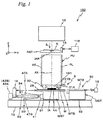
- Main controller 20 computes the position of reticle stage RST in the X-axis direction, Y-axis direction, and the ⁇ z direction based on the measurement values of reticle interferometer 116, and also controls the position (and velocity) of reticle stage RST by controlling reticle stage drive system 11 based on the computation results.
- the edge surface of reticle stage RST can be mirror polished so as to form a reflection surface (corresponding to the reflection surface of movable mirror 15).
- reticle interferometer 116 can measure positional information of reticle stage RST related to at least one of the Z-axis, ⁇ x, and ⁇ y directions.
- nozzle unit 32 is equipped with a supply opening and a recovery opening of liquid Lq, a lower surface to which wafer W is placed facing and at which the recovery opening is arranged, and a supply flow channel and a recovery flow channel that are connected to a liquid supply pipe 31A and a liquid recovery pipe 31B respectively.
- liquid supply pipe 31A and liquid recovery pipe 31B are inclined at an angle of 45 degrees with respect to the X-axis direction and the Y-axis direction in a planar view (when viewed from above) and are symmetrically placed with respect to a straight line LV in the Y-axis direction that passes through optical axis AX of projection optical system PL.
- One end of a supply pipe (not shown) is connected to liquid supply pipe 31A while the other end of the supply pipe is connected to a liquid supply device 5 (not shown in FIG. 1 , refer to FIG. 6 ), and one end of a recovery pipe (not shown) is connected to liquid recovery pipe 31B while the other end of the recovery pipe is connected to a liquid recovery device 6 (not shown in FIG. 1 , refer to FIG. 6 ).
- main controller 20 gives commands to the controllers of liquid supply device 5 and liquid recovery device 6 so that the quantity of water Lq supplied to the space between tip lens 191 and wafer W constantly equals the quantity of water Lq recovered from the space. Accordingly, a constant quantity of water Lq is held (refer to FIG. 1 ) in the space between tip lens 191 and wafer W. In this case, water Lq held in the space between tip lens 191 and wafer W is constantly replaced.
- stage drive system 124 is shown including each linear motor, the Z leveling mechanism, and the drive system of measurement stage MST described above. Further, wafer table WTB can also be configured finely movable in at least one of the X-axis, the Y-axis, and the ⁇ z directions.
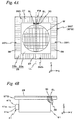
- plate 28 has a first liquid repellent area 28a whose outer shape (contour) is rectangular enclosing a circular opening, and a second liquid repellent area 28b that has a rectangular frame (annular) shape placed around the first liquid repellent area 28a.
- first liquid repellent area 28a for example, at the time of an exposure operation, at least a part of a liquid immersion area 14 that is protruded from the surface of the wafer is formed, and on the second liquid repellent area 28b, scales (grating sections) for an encoder system (to be described later) are formed.
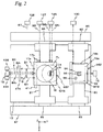
- main controller 20 can obtain the displacement of wafer stage WST in directions of six degrees of freedom (the Z, X, Y, ⁇ z, ⁇ x, and ⁇ y directions) in the entire stroke area from the measurement results of interferometer system 118 (refer to FIG. 6 ).
- interferometer system 118 includes X interferometers 126 to 128, Y interferometer 16, and Z interferometers 43A and 43B.
- each reflection surface measures the displacement of each reflection surface from a datum position (generally, a fixed mirror is placed on the side surface of projection unit PU, and the surface is used as a reference surface), that is, positional information of wafer stage WST within the XY plane, and positional information that has been measured is supplied to main controller 20.
- a datum position generally, a fixed mirror is placed on the side surface of projection unit PU, and the surface is used as a reference surface
- positional information of wafer stage WST within the XY plane positional information that has been measured is supplied to main controller 20.
- a multiaxial interferometer that has a plurality of measurement axes is used as each interferometer, with an exception for a part of the interferometers.
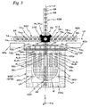
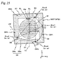
- a distance between adjacent X heads 66 (measurement beams) that are equipped in each of head units 62B and 62D is set shorter than a width in the Y-axis direction of X scales 39X 1 and 39X 2 (to be more accurate, a length of grid line 37).
- main controller 20 can measure a position coordinate of wafer stage WST in directions of three degree of freedom (X, Y, ⁇ z), in an effective stroke range of wafer stage WST, namely in an area where wafer stage WST moves for alignment and exposure operation.
- Each of the polarization directions of the two beams that have reached polarization beam splitter PBS is rotated at an angle of 90 degrees with respect to the original direction. Therefore, the first-order diffraction beam of beam LB 1 that was previously transmitted through polarization beam splitter PBS is reflected off polarization beam splitter PBS and is incident on photodetection system 64c, and also the first-order diffraction beam of beam LB 2 that was previously reflected off polarization beam splitter PBS is transmitted through polarization beam splitter PBS and is synthesized concentrically with the first-order diffraction beam of beam LB 1 described earlier and is incident on photodetection system 64c.
- characteristic information of the head unit which is a generation factor of the measurement error of the encoder system, includes not only the gradient of the head but also the optical properties as well.
- main controller 20 drives wafer stage WST so that Y scales 39Y 1 and 39Y 2 are located below head units 62A and 62C, respectively.
- Y head 64 A3 which is the third head from the left of head unit 62A
- Y head 64 C5 which is the second head from the right of head unit 62C
- main controller 20 drives wafer stage WST so that Y scales 39Y 1 and 39Y 2 are located below head units 62A and 62C, respectively.
- main controller 20 drives wafer stage WST if necessary in the X-axis direction, and makes a predetermined X head 66 of head units 62B and 62D face the specific area on X scales 39X 1 and 39X 2 where each X head 66 had faced when acquiring the stage position induced error correction information in the previous description.
- reflection surface 17b is to be an ideal plane.
- the correction information of the grating pitch and the grid line warp was acquired for both the Y scale and the X scale, however, the present invention is not limited to this, and the correction information of the grating pitch and the grid line warp can be acquired only for either the Y scale or the X scale, or the correction information of only either the grating pitch or the grid line warp can be acquired for both the Y scale and the X scale.
- wafer stage WST can be moved in the Y-axis direction based on the measurement values of Y linear encoders 70A and 70C, without necessarily using Y interferometer 16.
- the switching that could be performed from one combination of heads (encoders) to another combination of heads (encoders), and the timing when the switching can be performed are to be known, however, they also must be known in the actual sequence as well. It is also preferable to prepare the scheduling of the timing to carry out the linkage in advance.
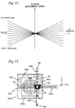
- Predicted value C Y4 that has been obtained is to be set as the initial value of the measurement value of the second head 64 4 at a proper timing. After the setting, the first head 64 3 is suspended when it moves off scale 39Y 2 , which completes the switching and linkage process.
- measurement table MTB and wafer table WTB can be separated, for example, at around 300 ⁇ m in the Y-axis direction while monitoring, for example, the measurement values of the interferometer or the encoder that measures the position of each table in the Y-axis direction so as to maintain a noncontact state (proximity state) .
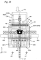
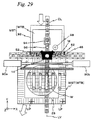
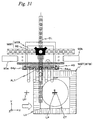
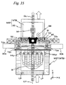
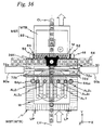
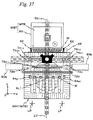
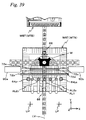
- wafer stage WST and measurement stage MST are set to the positional relation shown in FIG. 28 during the exposure of wafer W, both stages are moved while maintaining this positional relation.
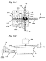
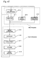
- main controller 20 detects the alignment marks arranged in the three first alignment shot areas substantially at the same time and also individually (refer to the star-shaped marks in FIG. 34 ), using primary alignment system AL1, and secondary alignment systems AL2 2 and AL2 3 , and makes a link between the detection results of the three alignment systems AL1, AL2 2 , and AL2 3 and the measurement values (measurement values after the correction according to each correction information) of at least the three encoders above at the time of the detection, and stores them in the internal memory.
- the Pri-BCHK latter process refers to a processing in which projected images (aerial images) of a pair of measurement marks on reticle R projected by projection optical system PL are measured, using aerial image measuring device 45 previously described which has aerial image measurement slit patterns SL formed on measurement plate 30, and the measurement results (aerial image intensity depending on the XY position of wafer table WTB) are stored in the internal memory.
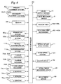
- main controller 20 takes in the output of each encoder (head) of the encoder system constantly (at a predetermined measurement sampling interval), as well as executes an operation where the encoder used for position control of wafer stage WST is switched from an encoder (head) that has been used for position control of wafer stage WST to another encoder (head) in synchronization with the timing of the position control of wafer stage WST. Therefore, the switching of the encoder no longer has to be performed at a high speed in synchronization with the measurement sampling where the output of the interferometer and the encoder is taken in, and a highly precise hardware for the switching will not be necessary, which consequently will make cost reduction possible.
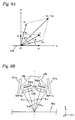
- wafer stage WST in the case of moving wafer stage WST in a predetermined direction, such as, for example, the Y-axis direction at the time of wafer alignment or exposure, wafer stage WST is driven in the Y-axis direction, based on the measurement information of the encoder system, the positional information (including inclination information, e.g., rotation information in the ⁇ x direction) of wafer stage WST in a direction different from the Y-axis direction, the characteristic information (e. g. the degree of flatness of the grating surface, and/or a grating formation error) of the scale, and the correction information of the Abbe error due to the Abbe offset quantity of the scale.
- the positional information including inclination information, e.g., rotation information in the ⁇ x direction
- the characteristic information e. g. the degree of flatness of the grating surface, and/or a grating formation error
- main controller 20 drives wafer stage WST in the Y-axis direction, based on the measurement values of encoders 70A and 70C which measure the positional information of wafer stage WST in a predetermined direction, such as, for example, in the Y-axis direction, the positional information of wafer stage WST in a direction different from the Y-axis direction at the time of the measurement (direction besides the measurement direction), such as, for example, the stage position induced error correction information (the correction information which is computed by formula (22) previously described) that corresponds to the positional information of wafer stage WST in the ⁇ x direction, ⁇ z direction, and the Z-axis direction measured by Y interferometer 16 and Z interferometers 43A and 43B of interferometer system 118, the correction information of the grating pitch of the Y scale (which is the correction information which takes into consideration the unevenness (degree of flatness) of the Y scale), the correction information of the warp of grid line 38 of the Y scale, and
- an encoder system that includes a total of three or more encoders including at least one each of a first encoder which measures positional information of the movable body in a direction that is parallel to a first axis within the movement plane and a second encoder which measures positional information of the movable body in a direction parallel to a second axis orthogonal to the first axis in the movement plane can be used by a controller, and the controller can switch an encoder used for measurement of the positional information of the movable body within the movement plane from an encoder of either of at least two encoders that include each one of the first encoder and the second encoder to another encoder, so as to maintain the position of the movable body within the movement plane before and after the switching.
- magnification of the projection optical system in the exposure apparatus of the embodiment above is not only a reduction system, but can also be either an equal magnifying system or a magnifying system
- projection optical system PL is not only a dioptric system, but can also be either a catoptric system or a catadioptric system
- the projected image may be either an inverted image or an upright image.
- the exposure area to which illumination light IL is irradiated via projection optical system PL is an on-axis area that includes optical axis AX within the field of projection optical system PL.
- the present invention can also be applied to an exposure apparatus that synthesizes two reticle patterns on a wafer via a projection optical system and almost simultaneously performs double exposure of one shot area on the wafer by one scanning exposure, as is disclosed in, for example, Kohyo (published Japanese translation of International Publication for Patent Application) No. 2004-519850 (the corresponding U.S. Patent No. 6,611,316 ).
Landscapes
- Physics & Mathematics (AREA)
- General Physics & Mathematics (AREA)
- Engineering & Computer Science (AREA)
- Multimedia (AREA)
- Public Health (AREA)
- Epidemiology (AREA)
- Environmental & Geological Engineering (AREA)
- Health & Medical Sciences (AREA)
- Exposure And Positioning Against Photoresist Photosensitive Materials (AREA)
- Exposure Of Semiconductors, Excluding Electron Or Ion Beam Exposure (AREA)
- Container, Conveyance, Adherence, Positioning, Of Wafer (AREA)
- Length Measuring Devices By Optical Means (AREA)
- Optical Transform (AREA)
Priority Applications (2)
| Application Number | Priority Date | Filing Date | Title |
|---|---|---|---|
| EP18184704.7A EP3418807A1 (fr) | 2006-08-31 | 2007-08-31 | Appareil d'exposition, procédé d'exposition et procédé de fabrication d'un dispositif |
| EP17200084.6A EP3312676B1 (fr) | 2006-08-31 | 2007-08-31 | Appareil d'exposition, procédé d'exposition et procédé de production d'un dispositif |
Applications Claiming Priority (4)
| Application Number | Priority Date | Filing Date | Title |
|---|---|---|---|
| JP2006237045 | 2006-08-31 | ||
| JP2006237491 | 2006-09-01 | ||
| JP2006237606 | 2006-09-01 | ||
| EP07806547.1A EP2065920B1 (fr) | 2006-08-31 | 2007-08-31 | Appareil d'exposition, procédé d'exposition et procédé de fabrication d'un dispositif |
Related Parent Applications (2)
| Application Number | Title | Priority Date | Filing Date |
|---|---|---|---|
| EP07806547.1A Division EP2065920B1 (fr) | 2006-08-31 | 2007-08-31 | Appareil d'exposition, procédé d'exposition et procédé de fabrication d'un dispositif |
| EP07806547.1A Division-Into EP2065920B1 (fr) | 2006-08-31 | 2007-08-31 | Appareil d'exposition, procédé d'exposition et procédé de fabrication d'un dispositif |
Related Child Applications (3)
| Application Number | Title | Priority Date | Filing Date |
|---|---|---|---|
| EP17200084.6A Division EP3312676B1 (fr) | 2006-08-31 | 2007-08-31 | Appareil d'exposition, procédé d'exposition et procédé de production d'un dispositif |
| EP17200084.6A Division-Into EP3312676B1 (fr) | 2006-08-31 | 2007-08-31 | Appareil d'exposition, procédé d'exposition et procédé de production d'un dispositif |
| EP18184704.7A Division EP3418807A1 (fr) | 2006-08-31 | 2007-08-31 | Appareil d'exposition, procédé d'exposition et procédé de fabrication d'un dispositif |
Publications (2)
| Publication Number | Publication Date |
|---|---|
| EP3067748A1 true EP3067748A1 (fr) | 2016-09-14 |
| EP3067748B1 EP3067748B1 (fr) | 2017-12-20 |
Family
ID=39136023
Family Applications (8)
| Application Number | Title | Priority Date | Filing Date |
|---|---|---|---|
| EP15182526.2A Not-in-force EP2993688B1 (fr) | 2006-08-31 | 2007-08-31 | Procédé et appareil d'exposition et procédé de fabrication d'un dispositif |
| EP18184704.7A Withdrawn EP3418807A1 (fr) | 2006-08-31 | 2007-08-31 | Appareil d'exposition, procédé d'exposition et procédé de fabrication d'un dispositif |
| EP16164422.4A Not-in-force EP3067748B1 (fr) | 2006-08-31 | 2007-08-31 | Appareil d'exposition, procédé d'exposition et procédé de fabrication d'un dispositif |
| EP07806547.1A Not-in-force EP2065920B1 (fr) | 2006-08-31 | 2007-08-31 | Appareil d'exposition, procédé d'exposition et procédé de fabrication d'un dispositif |
| EP15182527.0A Not-in-force EP2991101B1 (fr) | 2006-08-31 | 2007-08-31 | Procédé et appareil d'exposition et procédé de fabrication d'un dispositif |
| EP16163509.9A Not-in-force EP3064999B1 (fr) | 2006-08-31 | 2007-08-31 | Appareil d'exposition, procédé d'exposition et procédé de fabrication d'un dispositif |
| EP17200084.6A Not-in-force EP3312676B1 (fr) | 2006-08-31 | 2007-08-31 | Appareil d'exposition, procédé d'exposition et procédé de production d'un dispositif |
| EP14153959.3A Not-in-force EP2738608B9 (fr) | 2006-08-31 | 2007-08-31 | Système d'exposition et procédé d'exposition |
Family Applications Before (2)
| Application Number | Title | Priority Date | Filing Date |
|---|---|---|---|
| EP15182526.2A Not-in-force EP2993688B1 (fr) | 2006-08-31 | 2007-08-31 | Procédé et appareil d'exposition et procédé de fabrication d'un dispositif |
| EP18184704.7A Withdrawn EP3418807A1 (fr) | 2006-08-31 | 2007-08-31 | Appareil d'exposition, procédé d'exposition et procédé de fabrication d'un dispositif |
Family Applications After (5)
| Application Number | Title | Priority Date | Filing Date |
|---|---|---|---|
| EP07806547.1A Not-in-force EP2065920B1 (fr) | 2006-08-31 | 2007-08-31 | Appareil d'exposition, procédé d'exposition et procédé de fabrication d'un dispositif |
| EP15182527.0A Not-in-force EP2991101B1 (fr) | 2006-08-31 | 2007-08-31 | Procédé et appareil d'exposition et procédé de fabrication d'un dispositif |
| EP16163509.9A Not-in-force EP3064999B1 (fr) | 2006-08-31 | 2007-08-31 | Appareil d'exposition, procédé d'exposition et procédé de fabrication d'un dispositif |
| EP17200084.6A Not-in-force EP3312676B1 (fr) | 2006-08-31 | 2007-08-31 | Appareil d'exposition, procédé d'exposition et procédé de production d'un dispositif |
| EP14153959.3A Not-in-force EP2738608B9 (fr) | 2006-08-31 | 2007-08-31 | Système d'exposition et procédé d'exposition |
Country Status (9)
| Country | Link |
|---|---|
| US (6) | US20080094592A1 (fr) |
| EP (8) | EP2993688B1 (fr) |
| JP (13) | JP5035245B2 (fr) |
| KR (14) | KR101645909B1 (fr) |
| CN (3) | CN101405840B (fr) |
| HK (2) | HK1248325B (fr) |
| SG (2) | SG174091A1 (fr) |
| TW (8) | TWI596444B (fr) |
| WO (1) | WO2008026742A1 (fr) |
Families Citing this family (122)
| Publication number | Priority date | Publication date | Assignee | Title |
|---|---|---|---|---|
| EP2963498B8 (fr) | 2006-01-19 | 2017-07-26 | Nikon Corporation | Appareil d'exposition, procédé d'exposition et procédé de production d'un dispositif |
| EP3291010A1 (fr) * | 2006-08-31 | 2018-03-07 | Nikon Corporation | Appareil et procédé d'exposition et procédé de fabrication d'un dispositif |
| EP2993688B1 (fr) * | 2006-08-31 | 2017-04-05 | Nikon Corporation | Procédé et appareil d'exposition et procédé de fabrication d'un dispositif |
| KR101555793B1 (ko) * | 2006-08-31 | 2015-09-24 | 가부시키가이샤 니콘 | 이동체 구동 시스템 및 이동체 구동 방법, 패턴 형성 장치 및 방법, 노광 장치 및 방법, 디바이스 제조 방법, 그리고 결정 방법 |
| KR101660668B1 (ko) * | 2006-09-01 | 2016-09-27 | 가부시키가이샤 니콘 | 이동체 구동 방법 및 이동체 구동 시스템, 패턴 형성 방법 및 장치, 노광 방법 및 장치, 그리고 디바이스 제조 방법 |
| EP2993524B1 (fr) | 2006-09-01 | 2017-10-25 | Nikon Corporation | Procédé et appareil d'exposition et procédé de fabrication d'un dispositif |
| TWI475336B (zh) * | 2007-07-24 | 2015-03-01 | 尼康股份有限公司 | Mobile body driving method and moving body driving system, pattern forming method and apparatus, exposure method and apparatus, and component manufacturing method |
| US8237919B2 (en) * | 2007-08-24 | 2012-08-07 | Nikon Corporation | Movable body drive method and movable body drive system, pattern formation method and apparatus, exposure method and apparatus, and device manufacturing method for continuous position measurement of movable body before and after switching between sensor heads |
| US9013681B2 (en) * | 2007-11-06 | 2015-04-21 | Nikon Corporation | Movable body apparatus, pattern formation apparatus and exposure apparatus, and device manufacturing method |
| US9256140B2 (en) * | 2007-11-07 | 2016-02-09 | Nikon Corporation | Movable body apparatus, pattern formation apparatus and exposure apparatus, and device manufacturing method with measurement device to measure movable body in Z direction |
| US8665455B2 (en) * | 2007-11-08 | 2014-03-04 | Nikon Corporation | Movable body apparatus, pattern formation apparatus and exposure apparatus, and device manufacturing method |
| US8422015B2 (en) | 2007-11-09 | 2013-04-16 | Nikon Corporation | Movable body apparatus, pattern formation apparatus and exposure apparatus, and device manufacturing method |
| US8711327B2 (en) * | 2007-12-14 | 2014-04-29 | Nikon Corporation | Exposure apparatus, exposure method, and device manufacturing method |
| US8269945B2 (en) | 2007-12-28 | 2012-09-18 | Nikon Corporation | Movable body drive method and apparatus, exposure method and apparatus, pattern formation method and apparatus, and device manufacturing method |
| TWI454851B (zh) | 2007-12-28 | 2014-10-01 | 尼康股份有限公司 | An exposure apparatus, a moving body driving system, a pattern forming apparatus, and an exposure method, and an element manufacturing method |
| US8237916B2 (en) * | 2007-12-28 | 2012-08-07 | Nikon Corporation | Movable body drive system, pattern formation apparatus, exposure apparatus and exposure method, and device manufacturing method |
| US8792079B2 (en) * | 2007-12-28 | 2014-07-29 | Nikon Corporation | Exposure apparatus, exposure method, and device manufacturing method having encoders to measure displacement between optical member and measurement mount and between measurement mount and movable body |
| JP5126594B2 (ja) * | 2008-04-04 | 2013-01-23 | 株式会社ニコン | 較正方法、露光方法及びデバイス製造方法、並びに露光装置 |
| US8228482B2 (en) * | 2008-05-13 | 2012-07-24 | Nikon Corporation | Exposure apparatus, exposure method, and device manufacturing method |
| US8817236B2 (en) * | 2008-05-13 | 2014-08-26 | Nikon Corporation | Movable body system, movable body drive method, pattern formation apparatus, pattern formation method, exposure apparatus, exposure method, and device manufacturing method |
| US8786829B2 (en) * | 2008-05-13 | 2014-07-22 | Nikon Corporation | Exposure apparatus, exposure method, and device manufacturing method |
| US8994923B2 (en) * | 2008-09-22 | 2015-03-31 | Nikon Corporation | Movable body apparatus, exposure apparatus, exposure method, and device manufacturing method |
| JP5151852B2 (ja) * | 2008-09-22 | 2013-02-27 | 株式会社ニコン | 補正情報作成方法、露光方法及び露光装置、並びにデバイス製造方法 |
| US8325325B2 (en) | 2008-09-22 | 2012-12-04 | Nikon Corporation | Movable body apparatus, movable body drive method, exposure apparatus, exposure method, and device manufacturing method |
| US8508735B2 (en) * | 2008-09-22 | 2013-08-13 | Nikon Corporation | Movable body apparatus, movable body drive method, exposure apparatus, exposure method, and device manufacturing method |
| US8902402B2 (en) | 2008-12-19 | 2014-12-02 | Nikon Corporation | Movable body apparatus, exposure apparatus, exposure method, and device manufacturing method |
| US8760629B2 (en) | 2008-12-19 | 2014-06-24 | Nikon Corporation | Exposure apparatus including positional measurement system of movable body, exposure method of exposing object including measuring positional information of movable body, and device manufacturing method that includes exposure method of exposing object, including measuring positional information of movable body |
| US8599359B2 (en) | 2008-12-19 | 2013-12-03 | Nikon Corporation | Exposure apparatus, exposure method, device manufacturing method, and carrier method |
| US8773635B2 (en) * | 2008-12-19 | 2014-07-08 | Nikon Corporation | Exposure apparatus, exposure method, and device manufacturing method |
| US9531164B2 (en) | 2009-04-13 | 2016-12-27 | Soraa Laser Diode, Inc. | Optical device structure using GaN substrates for laser applications |
| US8837545B2 (en) | 2009-04-13 | 2014-09-16 | Soraa Laser Diode, Inc. | Optical device structure using GaN substrates and growth structures for laser applications |
| US8634442B1 (en) | 2009-04-13 | 2014-01-21 | Soraa Laser Diode, Inc. | Optical device structure using GaN substrates for laser applications |
| KR101636523B1 (ko) | 2009-05-20 | 2016-07-06 | 마퍼 리쏘그라피 아이피 비.브이. | 듀얼 패스 스캐닝 |
| US8792084B2 (en) * | 2009-05-20 | 2014-07-29 | Nikon Corporation | Exposure apparatus, exposure method, and device manufacturing method |
| US8553204B2 (en) * | 2009-05-20 | 2013-10-08 | Nikon Corporation | Movable body apparatus, exposure apparatus, exposure method, and device manufacturing method |
| US8970820B2 (en) * | 2009-05-20 | 2015-03-03 | Nikon Corporation | Object exchange method, exposure method, carrier system, exposure apparatus, and device manufacturing method |
| US8493547B2 (en) | 2009-08-25 | 2013-07-23 | Nikon Corporation | Exposure apparatus, exposure method, and device manufacturing method |
| US8514395B2 (en) | 2009-08-25 | 2013-08-20 | Nikon Corporation | Exposure method, exposure apparatus, and device manufacturing method |
| US8488109B2 (en) | 2009-08-25 | 2013-07-16 | Nikon Corporation | Exposure method, exposure apparatus, and device manufacturing method |
| WO2011031792A1 (fr) * | 2009-09-08 | 2011-03-17 | Im Chai S | Moteur à joint de culasse électromagnétique à séquencement de polarité et kit de remplacement associé |
| NL2005322A (en) * | 2009-09-11 | 2011-03-14 | Asml Netherlands Bv | A shutter member, a lithographic apparatus and device manufacturing method. |
| US20110096318A1 (en) * | 2009-09-28 | 2011-04-28 | Nikon Corporation | Exposure apparatus and device fabricating method |
| US20110102761A1 (en) * | 2009-09-28 | 2011-05-05 | Nikon Corporation | Stage apparatus, exposure apparatus, and device fabricating method |
| US20110096306A1 (en) * | 2009-09-28 | 2011-04-28 | Nikon Corporation | Stage apparatus, exposure apparatus, driving method, exposing method, and device fabricating method |
| US20110096312A1 (en) * | 2009-09-28 | 2011-04-28 | Nikon Corporation | Exposure apparatus and device fabricating method |
| US20110128523A1 (en) * | 2009-11-19 | 2011-06-02 | Nikon Corporation | Stage apparatus, exposure apparatus, driving method, exposing method, and device fabricating method |
| US20110123913A1 (en) * | 2009-11-19 | 2011-05-26 | Nikon Corporation | Exposure apparatus, exposing method, and device fabricating method |
| TWI402641B (zh) * | 2009-12-04 | 2013-07-21 | Ind Tech Res Inst | 聯結多系統達成多軸同步插值裝置與方法 |
| US8488106B2 (en) * | 2009-12-28 | 2013-07-16 | Nikon Corporation | Movable body drive method, movable body apparatus, exposure method, exposure apparatus, and device manufacturing method |
| NL2006004A (en) * | 2010-03-25 | 2011-09-27 | Asml Netherlands Bv | Imprint lithography. |
| NL2006913A (en) | 2010-07-16 | 2012-01-17 | Asml Netherlands Bv | Lithographic apparatus and method. |
| NL2007818A (en) | 2010-12-20 | 2012-06-21 | Asml Netherlands Bv | Method of updating calibration data and a device manufacturing method. |
| NL2007802A (en) | 2010-12-21 | 2012-06-25 | Asml Netherlands Bv | A substrate table, a lithographic apparatus and a device manufacturing method. |
| WO2012143541A1 (fr) | 2011-04-20 | 2012-10-26 | Mapper Lithography Ip B.V. | Structure de fibres optiques et son procédé de formation |
| US9207549B2 (en) | 2011-12-29 | 2015-12-08 | Nikon Corporation | Exposure apparatus and exposure method, and device manufacturing method with encoder of higher reliability for position measurement |
| EP2823361B1 (fr) | 2012-03-08 | 2022-03-02 | ASML Netherlands B.V. | Système de lithographie et procédé de traitement d'une cible, telle qu'une plaquette |
| US8779635B2 (en) * | 2012-04-10 | 2014-07-15 | Kla-Tencor Corporation | Arrangement of reticle positioning device for actinic inspection of EUV reticles |
| JP5936478B2 (ja) * | 2012-08-03 | 2016-06-22 | キヤノン株式会社 | 計測装置、リソグラフィー装置、および物品の製造方法 |
| JP5936479B2 (ja) * | 2012-08-03 | 2016-06-22 | キヤノン株式会社 | 計測装置、リソグラフィー装置、および物品の製造方法 |
| KR102203305B1 (ko) | 2012-10-02 | 2021-01-14 | 가부시키가이샤 니콘 | 노광 장치 및 노광 방법, 그리고 디바이스 제조 방법 |
| JP6243927B2 (ja) * | 2013-02-08 | 2017-12-06 | エーエスエムエル ネザーランズ ビー.ブイ. | リソグラフィ装置及びデバイス製造方法 |
| JP6381184B2 (ja) * | 2013-07-09 | 2018-08-29 | キヤノン株式会社 | 校正方法、測定装置、露光装置および物品の製造方法 |
| CN105684108A (zh) | 2013-09-04 | 2016-06-15 | Ckd株式会社 | 电磁致动器用电枢线圈、电磁致动器、曝光装置及器件制造方法 |
| JP6452086B2 (ja) * | 2013-10-31 | 2019-01-16 | キヤノン株式会社 | 形状算出装置及び方法、計測装置、物品製造方法、及び、プログラム |
| DE102014205523A1 (de) * | 2014-03-25 | 2015-10-01 | Etel S.A. | Positioniereinrichtung in Portalbauweise |
| US10534277B2 (en) * | 2014-03-26 | 2020-01-14 | Nikon Corporation | Movable body apparatus, exposure apparatus, manufacturing method of flat panel display, and device manufacturing method |
| TWI701514B (zh) | 2014-03-28 | 2020-08-11 | 日商尼康股份有限公司 | 移動體裝置、曝光裝置、平板顯示器之製造方法、元件製造方法、及移動體驅動方法 |
| JP6465565B2 (ja) | 2014-05-19 | 2019-02-06 | キヤノン株式会社 | 露光装置、位置合わせ方法およびデバイス製造方法 |
| JP6342738B2 (ja) * | 2014-07-24 | 2018-06-13 | 株式会社Screenホールディングス | データ補正装置、描画装置、検査装置、データ補正方法、描画方法、検査方法およびプログラム |
| WO2016030090A1 (fr) * | 2014-08-29 | 2016-03-03 | Asml Netherlands B.V. | Procédé d'étalonnage de système de codeur, système de positionnement d'objet, appareil lithographique, et procédé de fabrication de dispositif |
| KR102691584B1 (ko) | 2015-02-23 | 2024-08-05 | 가부시키가이샤 니콘 | 계측 장치, 리소그래피 시스템 및 노광 장치, 그리고 관리 방법, 중첩 계측 방법 및 디바이스 제조 방법 |
| EP3680717A1 (fr) | 2015-02-23 | 2020-07-15 | Nikon Corporation | Système de traitement de substrat et procédé de traitement de substrat, et procédé de fabrication de dispositif |
| KR102688211B1 (ko) | 2015-02-23 | 2024-07-24 | 가부시키가이샤 니콘 | 계측 장치, 리소그래피 시스템 및 노광 장치, 그리고 디바이스 제조 방법 |
| CN112415863B (zh) * | 2015-09-30 | 2023-05-23 | 株式会社尼康 | 曝光装置、平面显示器的制造方法、组件制造方法、及曝光方法 |
| KR102828061B1 (ko) * | 2015-09-30 | 2025-07-01 | 가부시키가이샤 니콘 | 이동체 장치, 노광 장치, 플랫 패널 디스플레이의 제조 방법, 및 디바이스 제조 방법, 그리고 계측 방법 |
| US10268121B2 (en) | 2015-09-30 | 2019-04-23 | Nikon Corporation | Exposure apparatus and exposure method, and flat panel display manufacturing method |
| US20180364595A1 (en) | 2015-09-30 | 2018-12-20 | Nikon Corporation | Exposure apparatus, flat panel display manufacturing method, and device manufacturing method |
| HK1248834A1 (zh) | 2015-09-30 | 2018-10-19 | 株式会社尼康 | 移动体装置、曝光装置、平面显示器的制造方法、及元件制造方法、以及物体的移动方法 |
| JP6885336B2 (ja) | 2015-09-30 | 2021-06-16 | 株式会社ニコン | 露光装置、露光方法、フラットパネルディスプレイの製造方法、及びデバイス製造方法 |
| KR102633248B1 (ko) | 2015-09-30 | 2024-02-02 | 가부시키가이샤 니콘 | 노광 장치 및 노광 방법, 그리고 플랫 패널 디스플레이 제조 방법 |
| HK1248832A1 (zh) | 2015-09-30 | 2018-10-19 | 株式会社尼康 | 曝光装置、平面显示器的制造方法、组件制造方法、及曝光方法 |
| JP6819887B2 (ja) | 2015-09-30 | 2021-01-27 | 株式会社ニコン | 露光装置及び露光方法、並びにフラットパネルディスプレイ製造方法 |
| US10732510B2 (en) * | 2015-09-30 | 2020-08-04 | Nikon Corporation | Exposure apparatus and exposure method, and flat panel display manufacturing method |
| CN108351598B (zh) * | 2015-10-27 | 2020-12-08 | Asml控股股份有限公司 | 与偏振无关的量测系统 |
| US10585357B2 (en) | 2015-12-28 | 2020-03-10 | Asml Netherlands B.V. | Alternative target design for metrology using modulation techniques |
| CN205427436U (zh) * | 2016-03-23 | 2016-08-03 | 北京京东方光电科技有限公司 | 显示器件的对位检测设备及曝光工艺系统 |
| JP6925783B2 (ja) * | 2016-05-26 | 2021-08-25 | 株式会社アドテックエンジニアリング | パターン描画装置及びパターン描画方法 |
| JP6438441B2 (ja) * | 2016-08-04 | 2018-12-12 | ファナック株式会社 | エンコーダの信号処理装置、エンコーダ、信号処理方法及びプログラム |
| EP3506012A4 (fr) * | 2016-08-24 | 2020-04-15 | Nikon Corporation | Système de mesure, système de traitement de substrat et procédé de fabrication de dispositif |
| CN110114725B (zh) | 2016-09-30 | 2021-09-17 | 株式会社尼康 | 搬运装置、曝光装置、平板显示器的制造方法、以及元件制造方法 |
| KR102291688B1 (ko) | 2016-09-30 | 2021-08-19 | 가부시키가이샤 니콘 | 노광 장치, 플랫 패널 디스플레이의 제조 방법, 디바이스 제조 방법, 및 노광 방법 |
| US10852647B2 (en) * | 2016-09-30 | 2020-12-01 | Nikon Corporation | Movable body apparatus, moving method, exposure apparatus, exposure method, flat-panel display manufacturing method , and device manufacturing method |
| CN109791366B (zh) * | 2016-09-30 | 2021-07-23 | 株式会社尼康 | 移动体装置、移动方法、曝光装置、曝光方法、平板显示器的制造方法、以及元件制造方法 |
| WO2018077873A1 (fr) * | 2016-10-27 | 2018-05-03 | Asml Netherlands B.V. | Système et procédé de détermination et d'étalonnage d'une position d'un étage |
| JP6711410B2 (ja) * | 2016-11-01 | 2020-06-17 | 株式会社島津製作所 | 放射線断層撮影装置の撮像倍率校正方法 |
| WO2018168708A1 (fr) * | 2017-03-14 | 2018-09-20 | パイオニア株式会社 | Dispositif d'affichage |
| US10877370B2 (en) * | 2017-07-31 | 2020-12-29 | Taiwan Semiconductor Manufacturing Co., Ltd. | Stretchable layout design for EUV defect mitigation |
| CN107806822B (zh) * | 2017-09-21 | 2020-06-09 | 中国科学院长春光学精密机械与物理研究所 | 一种测量装置 |
| CN107687814B (zh) * | 2017-09-21 | 2020-05-12 | 中国科学院长春光学精密机械与物理研究所 | 一种测量装置 |
| TWI663845B (zh) * | 2017-11-09 | 2019-06-21 | 美商Tt電子公司 | 光學編碼裝置及方法 |
| WO2019166879A1 (fr) * | 2018-03-02 | 2019-09-06 | Gooch & Housego Plc | Bague de montage pour maintenir l'alignement de dispositifs optiques |
| JP7137363B2 (ja) * | 2018-06-11 | 2022-09-14 | キヤノン株式会社 | 露光方法、露光装置、物品の製造方法及び計測方法 |
| DE102019210274A1 (de) * | 2019-07-11 | 2021-01-14 | Dr. Johannes Heidenhain Gmbh | Optische Positionsmesseinrichtung |
| US11764111B2 (en) * | 2019-10-24 | 2023-09-19 | Texas Instruments Incorporated | Reducing cross-wafer variability for minimum width resistors |
| CN113155053B (zh) | 2020-01-22 | 2024-09-06 | 株式会社三丰 | 三维几何形状测量装置和三维几何形状测量方法 |
| JP7360978B2 (ja) * | 2020-03-18 | 2023-10-13 | 株式会社日立ハイテクサイエンス | 荷電粒子ビーム装置 |
| CN111580455B (zh) * | 2020-06-05 | 2021-06-25 | 广东省智能制造研究所 | 一种数控设备的定位精度可靠性评估方法 |
| US11874144B2 (en) * | 2020-07-28 | 2024-01-16 | Li Lin | Displacement measurement system |
| JP7633044B2 (ja) * | 2021-03-09 | 2025-02-19 | 株式会社Screenホールディングス | 露光方法および露光装置 |
| JP7633045B2 (ja) * | 2021-03-09 | 2025-02-19 | 株式会社Screenホールディングス | 露光方法および露光装置 |
| JP7593482B2 (ja) * | 2021-04-09 | 2024-12-03 | 株式会社ニコン | 露光装置及び配線パターン形成方法 |
| JP2023000112A (ja) * | 2021-06-17 | 2023-01-04 | キオクシア株式会社 | 計測装置および計測プログラム |
| CN113552534B (zh) * | 2021-08-05 | 2022-02-01 | 中国人民解放军战略支援部队航天工程大学 | 基于脉冲信号的旋转基线干涉仪相位标校方法 |
| TWI791343B (zh) * | 2021-12-01 | 2023-02-01 | 財團法人工業技術研究院 | 旋轉軸的幾何誤差的獲取方法與獲取設備 |
| JP7834464B2 (ja) | 2021-12-13 | 2026-03-24 | キヤノン株式会社 | 搬送装置 |
| WO2024023885A1 (fr) * | 2022-07-25 | 2024-02-01 | 株式会社ニコン | Appareil d'exposition de motif et procédé de production de dispositif |
| CN115372365B (zh) * | 2022-09-30 | 2025-12-12 | 华东光电集成器件研究所 | 一种芯片测试装置 |
| KR102949195B1 (ko) | 2022-10-26 | 2026-04-08 | 삼성전자주식회사 | 기판 처리 장치 |
| CN115930808A (zh) * | 2022-12-13 | 2023-04-07 | 北京特种机械研究所 | 一种圆柱工件自动对准扫描系统及方法 |
| CN116674205B (zh) * | 2023-08-01 | 2023-12-15 | 易加三维增材技术(杭州)有限公司 | 位移控制方法、装置、非易失性存储介质及电子设备 |
| CN117733873B (zh) * | 2024-02-19 | 2024-04-19 | 深圳市德富莱智能科技股份有限公司 | 一种三维自动校准系统 |
| CN118565393B (zh) * | 2024-07-29 | 2024-10-18 | 汇丰金属科技(溧阳)有限公司 | 一种粉末冶金轴承精度检测装置 |
Citations (33)
| Publication number | Priority date | Publication date | Assignee | Title |
|---|---|---|---|---|
| JPS57117238A (en) | 1981-01-14 | 1982-07-21 | Nippon Kogaku Kk <Nikon> | Exposing and baking device for manufacturing integrated circuit with illuminometer |
| JPS6144429A (ja) | 1984-08-09 | 1986-03-04 | Nippon Kogaku Kk <Nikon> | 位置合わせ方法、及び位置合せ装置 |
| US4780617A (en) | 1984-08-09 | 1988-10-25 | Nippon Kogaku K.K. | Method for successive alignment of chip patterns on a substrate |
| EP0482553A2 (fr) * | 1990-10-22 | 1992-04-29 | Karl SÀ¼ss KG Präzisionsgeräte für Wissenschaft und Industrie - GmbH & Co. | Dispositif de mesure pour tables d'alignement x,y,gamma |
| JPH06283403A (ja) | 1993-03-26 | 1994-10-07 | Nikon Corp | 面位置設定装置 |
| US5448332A (en) | 1992-12-25 | 1995-09-05 | Nikon Corporation | Exposure method and apparatus |
| US5610715A (en) * | 1994-03-30 | 1997-03-11 | Canon Kabushiki Kaisha | Displacement detecting system, an expose apparatus, and a device manufacturing method employing a scale whose displacement is detected by a selected detection head |
| JPH10214783A (ja) | 1996-11-28 | 1998-08-11 | Nikon Corp | 投影露光装置及び投影露光方法 |
| WO1998040791A1 (fr) | 1997-03-10 | 1998-09-17 | Koninklijke Philips Electronics N.V. | Dispositif de positionnement pourvu de deux supports d'objet |
| JPH1116816A (ja) | 1997-06-25 | 1999-01-22 | Nikon Corp | 投影露光装置、該装置を用いた露光方法、及び該装置を用いた回路デバイスの製造方法 |
| WO1999046835A1 (fr) | 1998-03-11 | 1999-09-16 | Nikon Corporation | Dispositif a laser ultraviolet et appareil d'exposition comportant un tel dispositif a laser ultraviolet |
| WO1999049504A1 (fr) | 1998-03-26 | 1999-09-30 | Nikon Corporation | Procede et systeme d'exposition par projection |
| WO1999060361A1 (fr) | 1998-05-19 | 1999-11-25 | Nikon Corporation | Instrument et procede de mesure d'aberrations, appareil et procede de sensibilisation par projection incorporant cet instrument, et procede de fabrication de dispositifs associe |
| WO2001035168A1 (fr) | 1999-11-10 | 2001-05-17 | Massachusetts Institute Of Technology | Lithographie interferentielle utilisant des faisceaux de balayage a verrouillage de phase |
| JP2001313250A (ja) | 2000-02-25 | 2001-11-09 | Nikon Corp | 露光装置、その調整方法、及び前記露光装置を用いるデバイス製造方法 |
| JP2002014005A (ja) | 2000-04-25 | 2002-01-18 | Nikon Corp | 空間像計測方法、結像特性計測方法、空間像計測装置及び露光装置 |
| US6341007B1 (en) | 1996-11-28 | 2002-01-22 | Nikon Corporation | Exposure apparatus and method |
| US20020041377A1 (en) | 2000-04-25 | 2002-04-11 | Nikon Corporation | Aerial image measurement method and unit, optical properties measurement method and unit, adjustment method of projection optical system, exposure method and apparatus, making method of exposure apparatus, and device manufacturing method |
| JP2002151405A (ja) | 2000-08-24 | 2002-05-24 | Asm Lithography Bv | リトグラフィー投影装置 |
| US20030025890A1 (en) | 2000-02-25 | 2003-02-06 | Nikon Corporation | Exposure apparatus and exposure method capable of controlling illumination distribution |
| WO2003065428A1 (fr) | 2002-01-29 | 2003-08-07 | Nikon Corporation | Systeme de reglage d'etat de formation d'images, procede d'insolation, appareil d'exposition, programme, et support d'enregistrement d'information |
| US6611316B2 (en) | 2001-02-27 | 2003-08-26 | Asml Holding N.V. | Method and system for dual reticle image exposure |
| US6639686B1 (en) | 2000-04-13 | 2003-10-28 | Nanowave, Inc. | Method of and apparatus for real-time continual nanometer scale position measurement by beam probing as by laser beams and the like of atomic and other undulating surfaces such as gratings or the like relatively moving with respect to the probing beams |
| JP2004101362A (ja) | 2002-09-10 | 2004-04-02 | Canon Inc | ステージ位置計測および位置決め装置 |
| EP1420298A2 (fr) | 2002-11-12 | 2004-05-19 | ASML Netherlands B.V. | Appareil lithographique à immersion et méthode de fabrication d'un dispositif |
| WO2004053955A1 (fr) | 2002-12-10 | 2004-06-24 | Nikon Corporation | Systeme d'exposition et procede de production de dispositif |
| US6778257B2 (en) | 2001-07-24 | 2004-08-17 | Asml Netherlands B.V. | Imaging apparatus |
| WO2004107011A1 (fr) | 2003-05-06 | 2004-12-09 | Nikon Corporation | Systeme optique de projection et appareil d'exposition ainsi que procede d'exposition |
| WO2005074014A1 (fr) | 2004-02-02 | 2005-08-11 | Nikon Corporation | Proceded'entrainement d’etage et appareil d’entrainement d’etage, appareil d’exposition et procede de fabrication du dispositif |
| JP2005308592A (ja) | 2004-04-22 | 2005-11-04 | Sony Corp | 変位検出装置 |
| WO2005124834A1 (fr) | 2004-06-22 | 2005-12-29 | Nikon Corporation | Méthode de détection de la meilleure focalisation, méthode d’exposition et équipement d’exposition |
| EP1628163A2 (fr) * | 2004-08-19 | 2006-02-22 | ASML Netherlands BV | Appareil lithographique et méthode de fabrication d'un dispositif |
| WO2006038952A2 (fr) | 2004-09-30 | 2006-04-13 | Nikon Corporation | Dispositif optique de projection et appareil d'exposition |
Family Cites Families (177)
| Publication number | Priority date | Publication date | Assignee | Title |
|---|---|---|---|---|
| DE221563C (fr) | ||||
| US4465A (en) | 1846-04-18 | Improvement in plows | ||
| DE224448C (fr) | ||||
| US368A (en) | 1837-08-31 | John williamson | ||
| US4215938A (en) * | 1978-09-28 | 1980-08-05 | Farrand Industries, Inc. | Method and apparatus for correcting the error of a position measuring interferometer |
| US4346164A (en) * | 1980-10-06 | 1982-08-24 | Werner Tabarelli | Photolithographic method for the manufacture of integrated circuits |
| JPS57153433A (en) * | 1981-03-18 | 1982-09-22 | Hitachi Ltd | Manufacturing device for semiconductor |
| JPS58202448A (ja) | 1982-05-21 | 1983-11-25 | Hitachi Ltd | 露光装置 |
| JPS5919912A (ja) | 1982-07-26 | 1984-02-01 | Hitachi Ltd | 液浸距離保持装置 |
| DD221563A1 (de) | 1983-09-14 | 1985-04-24 | Mikroelektronik Zt Forsch Tech | Immersionsobjektiv fuer die schrittweise projektionsabbildung einer maskenstruktur |
| JPS60119407A (ja) * | 1983-11-30 | 1985-06-26 | Nippon Kogaku Kk <Nikon> | 比較検査装置 |
| DD224448A1 (de) | 1984-03-01 | 1985-07-03 | Zeiss Jena Veb Carl | Einrichtung zur fotolithografischen strukturuebertragung |
| JPS6265326A (ja) | 1985-09-18 | 1987-03-24 | Hitachi Ltd | 露光装置 |
| JPS63157419A (ja) | 1986-12-22 | 1988-06-30 | Toshiba Corp | 微細パタ−ン転写装置 |
| JPS63292005A (ja) * | 1987-05-25 | 1988-11-29 | Nikon Corp | 走り誤差補正をなした移動量検出装置 |
| US5489986A (en) * | 1989-02-28 | 1996-02-06 | Nikon Corporation | Position detecting apparatus |
| US5070250A (en) | 1989-02-28 | 1991-12-03 | Nikon Corporation | Position detection apparatus with adjustable beam and interference fringe positions |
| US5021649A (en) * | 1989-03-28 | 1991-06-04 | Canon Kabushiki Kaisha | Relief diffraction grating encoder |
| JP2784225B2 (ja) | 1989-11-28 | 1998-08-06 | 双葉電子工業株式会社 | 相対移動量測定装置 |
| JP3077149B2 (ja) * | 1990-01-22 | 2000-08-14 | 株式会社ニコン | 測定装置、測定方法、及び露光装置、露光方法、及び回路パターンチップ |
| US5523843A (en) * | 1990-07-09 | 1996-06-04 | Canon Kabushiki Kaisha | Position detecting system |
| JPH04305917A (ja) | 1991-04-02 | 1992-10-28 | Nikon Corp | 密着型露光装置 |
| JPH04305915A (ja) | 1991-04-02 | 1992-10-28 | Nikon Corp | 密着型露光装置 |
| US5506684A (en) | 1991-04-04 | 1996-04-09 | Nikon Corporation | Projection scanning exposure apparatus with synchronous mask/wafer alignment system |
| JP3149472B2 (ja) * | 1991-08-30 | 2001-03-26 | 株式会社ニコン | 走査露光装置および物体の移動測定装置 |
| JP3030386B2 (ja) | 1991-05-15 | 2000-04-10 | 敏一 中村 | 抗ガン剤 |
| DE4219311C2 (de) * | 1991-06-13 | 1996-03-07 | Sony Magnescale Inc | Verschiebungsdetektor |
| JPH0562877A (ja) | 1991-09-02 | 1993-03-12 | Yasuko Shinohara | 光によるlsi製造縮小投影露光装置の光学系 |
| JPH05129184A (ja) * | 1991-10-30 | 1993-05-25 | Canon Inc | 投影露光装置 |
| JPH05173639A (ja) * | 1991-12-20 | 1993-07-13 | Fujitsu Ltd | 位置制御装置及びその制御方法 |
| JPH06124873A (ja) | 1992-10-09 | 1994-05-06 | Canon Inc | 液浸式投影露光装置 |
| JP2753930B2 (ja) * | 1992-11-27 | 1998-05-20 | キヤノン株式会社 | 液浸式投影露光装置 |
| JP3303386B2 (ja) | 1993-02-03 | 2002-07-22 | 株式会社ニコン | 投影露光装置及び方法 |
| US5461237A (en) * | 1993-03-26 | 1995-10-24 | Nikon Corporation | Surface-position setting apparatus |
| US5583609A (en) | 1993-04-23 | 1996-12-10 | Nikon Corporation | Projection exposure apparatus |
| JP3309871B2 (ja) * | 1993-04-27 | 2002-07-29 | 株式会社ニコン | 投影露光方法及び装置、並びに素子製造方法 |
| JP3375076B2 (ja) | 1993-04-27 | 2003-02-10 | 株式会社ニコン | 投影露光方法及び装置、並びに素子製造方法 |
| US5581324A (en) | 1993-06-10 | 1996-12-03 | Nikon Corporation | Thermal distortion compensated projection exposure method and apparatus for manufacturing semiconductors |
| JP3319819B2 (ja) * | 1993-06-25 | 2002-09-03 | 株式会社リコー | 画像形成装置管理システム |
| US6122036A (en) | 1993-10-21 | 2000-09-19 | Nikon Corporation | Projection exposure apparatus and method |
| JPH09223650A (ja) | 1996-02-15 | 1997-08-26 | Nikon Corp | 露光装置 |
| US5625453A (en) * | 1993-10-26 | 1997-04-29 | Canon Kabushiki Kaisha | System and method for detecting the relative positional deviation between diffraction gratings and for measuring the width of a line constituting a diffraction grating |
| JP3382389B2 (ja) * | 1993-10-26 | 2003-03-04 | キヤノン株式会社 | 位置ずれ検出方法及びそれを用いた位置ずれ検出装置 |
| JPH07190741A (ja) * | 1993-12-27 | 1995-07-28 | Nippon Telegr & Teleph Corp <Ntt> | 測定誤差補正法 |
| JPH07220990A (ja) | 1994-01-28 | 1995-08-18 | Hitachi Ltd | パターン形成方法及びその露光装置 |
| JPH07318699A (ja) * | 1994-05-27 | 1995-12-08 | Canon Inc | ステージ装置及びこれを有する露光装置とデバイス製造方法 |
| US6018384A (en) | 1994-09-07 | 2000-01-25 | Nikon Corporation | Projection exposure system |
| JP3379238B2 (ja) | 1994-09-08 | 2003-02-24 | 株式会社ニコン | 走査型露光装置 |
| JPH0883753A (ja) * | 1994-09-13 | 1996-03-26 | Nikon Corp | 焦点検出方法 |
| JPH08316125A (ja) | 1995-05-19 | 1996-11-29 | Hitachi Ltd | 投影露光方法及び露光装置 |
| JPH08316124A (ja) * | 1995-05-19 | 1996-11-29 | Hitachi Ltd | 投影露光方法及び露光装置 |
| JPH09115820A (ja) * | 1995-10-13 | 1997-05-02 | Nikon Corp | 走査型露光装置及び露光方法 |
| JPH09318321A (ja) * | 1996-05-30 | 1997-12-12 | Olympus Optical Co Ltd | 測長装置 |
| JPH1022218A (ja) * | 1996-07-02 | 1998-01-23 | Nikon Corp | 基板のアライメント方法 |
| CN101324825B (zh) * | 1996-08-12 | 2012-05-30 | 蒂科电子公司 | 利用多个互不正交的波的声学条件传感器 |
| JPH1063011A (ja) | 1996-08-14 | 1998-03-06 | Nikon Corp | 走査型露光装置及び走査露光方法 |
| US5917580A (en) * | 1996-08-29 | 1999-06-29 | Canon Kabushiki Kaisha | Scan exposure method and apparatus |
| US5825043A (en) * | 1996-10-07 | 1998-10-20 | Nikon Precision Inc. | Focusing and tilting adjustment system for lithography aligner, manufacturing apparatus or inspection apparatus |
| JPH10223528A (ja) | 1996-12-30 | 1998-08-21 | Nikon Corp | 投影露光装置及び位置合わせ方法 |
| JP3963037B2 (ja) * | 1997-03-19 | 2007-08-22 | ソニー株式会社 | 記録装置及び再生装置 |
| JPH10270535A (ja) | 1997-03-25 | 1998-10-09 | Nikon Corp | 移動ステージ装置、及び該ステージ装置を用いた回路デバイス製造方法 |
| JP3747566B2 (ja) | 1997-04-23 | 2006-02-22 | 株式会社ニコン | 液浸型露光装置 |
| JP3817836B2 (ja) | 1997-06-10 | 2006-09-06 | 株式会社ニコン | 露光装置及びその製造方法並びに露光方法及びデバイス製造方法 |
| JPH11121325A (ja) * | 1997-09-03 | 1999-04-30 | Canon Inc | 投影露光装置 |
| JP4210871B2 (ja) * | 1997-10-31 | 2009-01-21 | 株式会社ニコン | 露光装置 |
| US6020964A (en) | 1997-12-02 | 2000-02-01 | Asm Lithography B.V. | Interferometer system and lithograph apparatus including an interferometer system |
| JPH11176727A (ja) | 1997-12-11 | 1999-07-02 | Nikon Corp | 投影露光装置 |
| JP3809268B2 (ja) | 1997-12-19 | 2006-08-16 | キヤノン株式会社 | デバイス製造方法 |
| JPH11191585A (ja) * | 1997-12-26 | 1999-07-13 | Canon Inc | ステージ装置、およびこれを用いた露光装置、ならびにデバイス製造方法 |
| JPH11233420A (ja) | 1998-02-18 | 1999-08-27 | Nikon Corp | 投影露光装置及び位置検出方法 |
| US6008610A (en) | 1998-03-20 | 1999-12-28 | Nikon Corporation | Position control apparatus for fine stages carried by a coarse stage on a high-precision scanning positioning system |
| JP2000058436A (ja) | 1998-08-11 | 2000-02-25 | Nikon Corp | 投影露光装置及び露光方法 |
| JP2000068192A (ja) | 1998-08-18 | 2000-03-03 | Nikon Corp | 露光装置、露光方法及び位置検出方法 |
| US6144118A (en) * | 1998-09-18 | 2000-11-07 | General Scanning, Inc. | High-speed precision positioning apparatus |
| DE69943311D1 (de) | 1998-12-24 | 2011-05-12 | Canon Kk | Trägerplattesteuerungsvorrichtung, Belichtungsapparat und Verfahren zur Herstellung einer Halbleitervorrichtung |
| US6924884B2 (en) * | 1999-03-08 | 2005-08-02 | Asml Netherlands B.V. | Off-axis leveling in lithographic projection apparatus |
| TW490596B (en) * | 1999-03-08 | 2002-06-11 | Asm Lithography Bv | Lithographic projection apparatus, method of manufacturing a device using the lithographic projection apparatus, device manufactured according to the method and method of calibrating the lithographic projection apparatus |
| US6381004B1 (en) * | 1999-09-29 | 2002-04-30 | Nikon Corporation | Exposure apparatus and device manufacturing method |
| JP2001118768A (ja) * | 1999-10-15 | 2001-04-27 | Nikon Corp | マスクのアライメント方法および露光装置 |
| JP4428781B2 (ja) | 1999-12-28 | 2010-03-10 | キヤノン株式会社 | 光学式ロータリエンコーダ及びモータ制御装置 |
| WO2001052004A1 (fr) * | 2000-01-11 | 2001-07-19 | Electro Scientific Industries, Inc. | Systeme et procede de correction d'erreurs d'abbe |
| JP2001308003A (ja) * | 2000-02-15 | 2001-11-02 | Nikon Corp | 露光方法及び装置、並びにデバイス製造方法 |
| JP2001332490A (ja) * | 2000-03-14 | 2001-11-30 | Nikon Corp | 位置合わせ方法、露光方法、露光装置、及びデバイス製造方法 |
| US6970245B2 (en) * | 2000-08-02 | 2005-11-29 | Honeywell International Inc. | Optical alignment detection system |
| JP2002090114A (ja) * | 2000-07-10 | 2002-03-27 | Mitsutoyo Corp | 光スポット位置センサ及び変位測定装置 |
| JP2002031895A (ja) | 2000-07-18 | 2002-01-31 | Nikon Corp | 露光装置 |
| US7289212B2 (en) * | 2000-08-24 | 2007-10-30 | Asml Netherlands B.V. | Lithographic apparatus, device manufacturing method and device manufacturing thereby |
| US7561270B2 (en) * | 2000-08-24 | 2009-07-14 | Asml Netherlands B.V. | Lithographic apparatus, device manufacturing method and device manufactured thereby |
| US6557190B2 (en) | 2001-08-31 | 2003-05-06 | National Rv Holdings, Inc. | Storable bed assembly |
| JP2002164269A (ja) * | 2000-11-27 | 2002-06-07 | Nikon Corp | 露光方法及び装置、並びにデバイス製造方法 |
| WO2002078388A2 (fr) | 2001-03-27 | 2002-10-03 | 1... Limited | Procede et appareil permettant de creer un champ acoustique |
| JP2002305140A (ja) * | 2001-04-06 | 2002-10-18 | Nikon Corp | 露光装置及び基板処理システム |
| JP4198338B2 (ja) * | 2001-07-09 | 2008-12-17 | 株式会社 東北テクノアーチ | ステージ装置 |
| JP2003031474A (ja) * | 2001-07-16 | 2003-01-31 | Oki Electric Ind Co Ltd | 露光装置および露光方法 |
| KR20010112204A (ko) * | 2001-12-01 | 2001-12-20 | 엄경미 | 위생패드 |
| JP2003249443A (ja) | 2001-12-21 | 2003-09-05 | Nikon Corp | ステージ装置、ステージ位置管理方法、露光方法及び露光装置、並びにデバイス製造方法 |
| US6987555B2 (en) * | 2002-04-23 | 2006-01-17 | Asml Netherlands B.V. | Lithographic apparatus, device manufacturing method, and device manufactured thereby |
| JP4168665B2 (ja) | 2002-05-22 | 2008-10-22 | 株式会社ニコン | 露光方法及び露光装置、デバイス製造方法 |
| JP2004014876A (ja) * | 2002-06-07 | 2004-01-15 | Nikon Corp | 調整方法、空間像計測方法及び像面計測方法、並びに露光装置 |
| JP3833148B2 (ja) * | 2002-06-25 | 2006-10-11 | キヤノン株式会社 | 位置決め装置及びその制御方法、露光装置、デバイスの製造方法、半導体製造工場、露光装置の保守方法 |
| JP2004041362A (ja) | 2002-07-10 | 2004-02-12 | Sankyo Kk | 弾球遊技機およびスロットマシン |
| KR20050025626A (ko) * | 2002-07-31 | 2005-03-14 | 가부시키가이샤 니콘 | 위치계측방법, 위치제어방법, 노광방법 및 노광장치,그리고 디바이스 제조방법 |
| WO2004019128A2 (fr) | 2002-08-23 | 2004-03-04 | Nikon Corporation | Systeme optique de projection et procede associe pour la photolithographie, et appareil d'exposition et procede associe |
| TWI229243B (en) * | 2002-09-20 | 2005-03-11 | Asml Netherlands Bv | Lithographic marker structure, lithographic projection apparatus comprising such a lithographic marker structure and method for substrate alignment using such a lithographic marker structure |
| CN1245668C (zh) * | 2002-10-14 | 2006-03-15 | 台湾积体电路制造股份有限公司 | 曝光系统及其曝光方法 |
| CN101470360B (zh) * | 2002-11-12 | 2013-07-24 | Asml荷兰有限公司 | 光刻装置和器件制造方法 |
| DE60335595D1 (de) | 2002-11-12 | 2011-02-17 | Asml Netherlands Bv | Lithographischer Apparat mit Immersion und Verfahren zur Herstellung einer Vorrichtung |
| US7393804B2 (en) * | 2002-11-18 | 2008-07-01 | Ict Co., Ltd. | Exhaust gas purifying catalyst and process for purification of exhaust gas |
| AU2003289146A1 (en) * | 2002-12-03 | 2004-06-23 | Nikon Corporation | Shape measurement method, shape measurement device, tilt measurement method, stage device, exposure device, exposure method, and device manufacturing method |
| EP1571696A4 (fr) * | 2002-12-10 | 2008-03-26 | Nikon Corp | Dispositif d'exposition, et procede de fabrication |
| KR101177330B1 (ko) | 2003-04-10 | 2012-08-30 | 가부시키가이샤 니콘 | 액침 리소그래피 장치 |
| SG139733A1 (en) * | 2003-04-11 | 2008-02-29 | Nikon Corp | Apparatus having an immersion fluid system configured to maintain immersion fluid in a gap adjacent an optical assembly |
| US7025498B2 (en) * | 2003-05-30 | 2006-04-11 | Asml Holding N.V. | System and method of measuring thermal expansion |
| KR101931923B1 (ko) * | 2003-06-19 | 2018-12-21 | 가부시키가이샤 니콘 | 노광 장치 및 디바이스 제조방법 |
| US20050027487A1 (en) * | 2003-07-15 | 2005-02-03 | Supriya Iyer | Product defect analysis and resolution system |
| JP4492239B2 (ja) * | 2003-07-28 | 2010-06-30 | 株式会社ニコン | 露光装置及びデバイス製造方法、並びに露光装置の制御方法 |
| KR101642670B1 (ko) | 2003-07-28 | 2016-07-25 | 가부시키가이샤 니콘 | 노광 장치 및 디바이스 제조 방법, 그리고 노광 장치의 제어 방법 |
| KR101259095B1 (ko) * | 2003-08-21 | 2013-04-30 | 가부시키가이샤 니콘 | 노광 장치, 노광 방법 및 디바이스 제조 방법 |
| JP4524601B2 (ja) * | 2003-10-09 | 2010-08-18 | 株式会社ニコン | 露光装置及び露光方法、デバイス製造方法 |
| TWI295408B (en) * | 2003-10-22 | 2008-04-01 | Asml Netherlands Bv | Lithographic apparatus and device manufacturing method, and measurement system |
| JP2005159322A (ja) * | 2003-10-31 | 2005-06-16 | Nikon Corp | 定盤、ステージ装置及び露光装置並びに露光方法 |
| US7102729B2 (en) * | 2004-02-03 | 2006-09-05 | Asml Netherlands B.V. | Lithographic apparatus, measurement system, and device manufacturing method |
| JP2005252246A (ja) | 2004-02-04 | 2005-09-15 | Nikon Corp | 露光装置及び方法、位置制御方法、並びにデバイス製造方法 |
| WO2005076325A1 (fr) | 2004-02-04 | 2005-08-18 | Nikon Corporation | Equipement et procede d’exposition, procede de reglage de la position et procede de fabrication d’un dispositif |
| JP4429037B2 (ja) * | 2004-02-27 | 2010-03-10 | キヤノン株式会社 | ステージ装置及びその制御方法 |
| JP2005249452A (ja) | 2004-03-02 | 2005-09-15 | Konica Minolta Medical & Graphic Inc | リニアエンコーダ、画像読取装置及び画像記録装置 |
| JP4622340B2 (ja) | 2004-03-04 | 2011-02-02 | 株式会社ニコン | 露光装置、デバイス製造方法 |
| JP2005268608A (ja) * | 2004-03-19 | 2005-09-29 | Sumitomo Heavy Ind Ltd | ステージ装置 |
| JP2005283357A (ja) * | 2004-03-30 | 2005-10-13 | Sendai Nikon:Kk | 光電式エンコーダ |
| US7898642B2 (en) | 2004-04-14 | 2011-03-01 | Asml Netherlands B.V. | Lithographic apparatus and device manufacturing method |
| US20050241694A1 (en) | 2004-04-29 | 2005-11-03 | Red Flame Hot Tap Services Ltd. | Hot tapping method, system and apparatus |
| US7126109B2 (en) | 2004-06-14 | 2006-10-24 | Gsi Group Corporation | Encoder scale error compensation employing comparison among multiple detectors |
| US20060013959A1 (en) * | 2004-07-15 | 2006-01-19 | Morales Hector D | Process to apply a polimeric coating on non-ferrous substrates |
| US7256871B2 (en) | 2004-07-27 | 2007-08-14 | Asml Netherlands B.V. | Lithographic apparatus and method for calibrating the same |
| TWI610340B (zh) | 2004-09-17 | 2018-01-01 | 尼康股份有限公司 | 曝光裝置、曝光方法及元件製造方法 |
| JP4852951B2 (ja) * | 2004-09-17 | 2012-01-11 | 株式会社ニコン | 露光装置、露光方法及びデバイス製造方法 |
| SG156635A1 (en) * | 2004-10-15 | 2009-11-26 | Nikon Corp | Exposure apparatus and device manufacturing method |
| JP4424739B2 (ja) | 2004-10-19 | 2010-03-03 | キヤノン株式会社 | ステージ装置 |
| US7388663B2 (en) * | 2004-10-28 | 2008-06-17 | Asml Netherlands B.V. | Optical position assessment apparatus and method |
| EP2472332B1 (fr) * | 2004-11-01 | 2014-03-12 | Nikon Corporation | Appareil d'exposition et méthode de fabrication d'un dispositif |
| TWI588872B (zh) * | 2004-11-18 | 2017-06-21 | 尼康股份有限公司 | Position measurement method, position control method, measurement method, loading method, exposure method and exposure apparatus, and device manufacturing method |
| WO2006057263A1 (fr) | 2004-11-25 | 2006-06-01 | Nikon Corporation | Systeme de corps mobile, appareil d’exposition et procede de production du dispositif |
| US20060139595A1 (en) * | 2004-12-27 | 2006-06-29 | Asml Netherlands B.V. | Lithographic apparatus and method for determining Z position errors/variations and substrate table flatness |
| JP4450739B2 (ja) | 2005-01-21 | 2010-04-14 | 富士フイルム株式会社 | 露光装置 |
| JP2006210570A (ja) | 2005-01-27 | 2006-08-10 | Nikon Corp | 調整方法、露光装置 |
| US7161659B2 (en) * | 2005-04-08 | 2007-01-09 | Asml Netherlands B.V. | Dual stage lithographic apparatus and device manufacturing method |
| US7515281B2 (en) * | 2005-04-08 | 2009-04-07 | Asml Netherlands B.V. | Lithographic apparatus and device manufacturing method |
| US7349069B2 (en) * | 2005-04-20 | 2008-03-25 | Asml Netherlands B.V. | Lithographic apparatus and positioning apparatus |
| US7405811B2 (en) * | 2005-04-20 | 2008-07-29 | Asml Netherlands B.V. | Lithographic apparatus and positioning apparatus |
| JP2007054987A (ja) * | 2005-08-23 | 2007-03-08 | Soshiodaiya Systems Kk | 印刷装置及び印刷方法 |
| US7348574B2 (en) * | 2005-09-02 | 2008-03-25 | Asml Netherlands, B.V. | Position measurement system and lithographic apparatus |
| US7362446B2 (en) * | 2005-09-15 | 2008-04-22 | Asml Netherlands B.V. | Position measurement unit, measurement system and lithographic apparatus comprising such position measurement unit |
| JP2007093546A (ja) * | 2005-09-30 | 2007-04-12 | Nikon Corp | エンコーダシステム、ステージ装置及び露光装置 |
| US7978339B2 (en) * | 2005-10-04 | 2011-07-12 | Asml Netherlands B.V. | Lithographic apparatus temperature compensation |
| JP4164508B2 (ja) * | 2005-10-04 | 2008-10-15 | キヤノン株式会社 | 露光装置及びデバイス製造方法 |
| EP2963498B8 (fr) | 2006-01-19 | 2017-07-26 | Nikon Corporation | Appareil d'exposition, procédé d'exposition et procédé de production d'un dispositif |
| KR20090015888A (ko) * | 2006-02-21 | 2009-02-12 | 가부시키가이샤 니콘 | 위치 계측 장치 및 위치 계측 방법, 이동체 구동 시스템 및이동체 구동 방법, 패턴 형성 장치 및 패턴 형성 방법, 노광 장치 및 노광 방법, 그리고 디바이스 제조 방법 |
| EP2003680B1 (fr) | 2006-02-21 | 2013-05-29 | Nikon Corporation | Appareil d'exposition, procédé d'exposition et procédé de fabrication d'un dispositif |
| EP3115844B1 (fr) * | 2006-02-21 | 2018-08-15 | Nikon Corporation | Appareil d'exposition, procédé d'exposition et procédé de fabrication d'un dispositif |
| EP2003681B1 (fr) * | 2006-02-21 | 2014-11-12 | Nikon Corporation | Procédé et dispositif de mesure, procédé et dispositif de formation de motifs, et procédé de fabrication des dispositifs |
| US7602489B2 (en) * | 2006-02-22 | 2009-10-13 | Asml Netherlands B.V. | Lithographic apparatus and device manufacturing method |
| US7253875B1 (en) * | 2006-03-03 | 2007-08-07 | Asml Netherlands B.V. | Lithographic apparatus and device manufacturing method |
| US7636165B2 (en) * | 2006-03-21 | 2009-12-22 | Asml Netherlands B.V. | Displacement measurement systems lithographic apparatus and device manufacturing method |
| US7576832B2 (en) | 2006-05-04 | 2009-08-18 | Asml Netherlands B.V. | Lithographic apparatus and device manufacturing method |
| US7483120B2 (en) * | 2006-05-09 | 2009-01-27 | Asml Netherlands B.V. | Displacement measurement system, lithographic apparatus, displacement measurement method and device manufacturing method |
| JP4393540B2 (ja) | 2006-08-01 | 2010-01-06 | シャープ株式会社 | 樹脂含有粒子の凝集体の製造方法、トナー、現像剤、現像装置および画像形成装置 |
| US20080050680A1 (en) * | 2006-08-24 | 2008-02-28 | Stefan Brandl | Lithography systems and methods |
| KR101555793B1 (ko) * | 2006-08-31 | 2015-09-24 | 가부시키가이샤 니콘 | 이동체 구동 시스템 및 이동체 구동 방법, 패턴 형성 장치 및 방법, 노광 장치 및 방법, 디바이스 제조 방법, 그리고 결정 방법 |
| EP3291010A1 (fr) | 2006-08-31 | 2018-03-07 | Nikon Corporation | Appareil et procédé d'exposition et procédé de fabrication d'un dispositif |
| EP2993688B1 (fr) * | 2006-08-31 | 2017-04-05 | Nikon Corporation | Procédé et appareil d'exposition et procédé de fabrication d'un dispositif |
| EP2993524B1 (fr) * | 2006-09-01 | 2017-10-25 | Nikon Corporation | Procédé et appareil d'exposition et procédé de fabrication d'un dispositif |
| KR101660668B1 (ko) * | 2006-09-01 | 2016-09-27 | 가부시키가이샤 니콘 | 이동체 구동 방법 및 이동체 구동 시스템, 패턴 형성 방법 및 장치, 노광 방법 및 장치, 그리고 디바이스 제조 방법 |
| US7619207B2 (en) * | 2006-11-08 | 2009-11-17 | Asml Netherlands B.V. | Lithographic apparatus and device manufacturing method |
| US7903866B2 (en) | 2007-03-29 | 2011-03-08 | Asml Netherlands B.V. | Measurement system, lithographic apparatus and method for measuring a position dependent signal of a movable object |
| US7710540B2 (en) * | 2007-04-05 | 2010-05-04 | Asml Netherlands B.V. | Lithographic apparatus and device manufacturing method |
| US8547527B2 (en) * | 2007-07-24 | 2013-10-01 | Nikon Corporation | Movable body drive method and movable body drive system, pattern formation method and pattern formation apparatus, and device manufacturing method |
| TWI454851B (zh) * | 2007-12-28 | 2014-10-01 | 尼康股份有限公司 | An exposure apparatus, a moving body driving system, a pattern forming apparatus, and an exposure method, and an element manufacturing method |
-
2007
- 2007-08-31 EP EP15182526.2A patent/EP2993688B1/fr not_active Not-in-force
- 2007-08-31 EP EP18184704.7A patent/EP3418807A1/fr not_active Withdrawn
- 2007-08-31 TW TW105100233A patent/TWI596444B/zh not_active IP Right Cessation
- 2007-08-31 KR KR1020157019884A patent/KR101645909B1/ko not_active Expired - Fee Related
- 2007-08-31 KR KR1020157036552A patent/KR101698291B1/ko not_active Expired - Fee Related
- 2007-08-31 TW TW102132750A patent/TWI537687B/zh not_active IP Right Cessation
- 2007-08-31 KR KR1020137020821A patent/KR101477448B1/ko not_active Expired - Fee Related
- 2007-08-31 KR KR1020147034199A patent/KR101565275B1/ko not_active Expired - Fee Related
- 2007-08-31 EP EP16164422.4A patent/EP3067748B1/fr not_active Not-in-force
- 2007-08-31 KR KR1020187036725A patent/KR20180137600A/ko not_active Ceased
- 2007-08-31 KR KR1020087026015A patent/KR101400615B1/ko not_active Expired - Fee Related
- 2007-08-31 TW TW102132751A patent/TWI529501B/zh not_active IP Right Cessation
- 2007-08-31 CN CN2007800102592A patent/CN101405840B/zh not_active Expired - Fee Related
- 2007-08-31 CN CN201110384985.9A patent/CN102520588B/zh not_active Expired - Fee Related
- 2007-08-31 WO PCT/JP2007/067074 patent/WO2008026742A1/fr not_active Ceased
- 2007-08-31 SG SG2011060241A patent/SG174091A1/en unknown
- 2007-08-31 TW TW106129977A patent/TWI653511B/zh not_active IP Right Cessation
- 2007-08-31 KR KR1020177000847A patent/KR101824374B1/ko not_active Expired - Fee Related
- 2007-08-31 EP EP07806547.1A patent/EP2065920B1/fr not_active Not-in-force
- 2007-08-31 JP JP2008532138A patent/JP5035245B2/ja not_active Expired - Fee Related
- 2007-08-31 TW TW105100234A patent/TWI649631B/zh not_active IP Right Cessation
- 2007-08-31 SG SG10201407395SA patent/SG10201407395SA/en unknown
- 2007-08-31 KR KR1020187002349A patent/KR101933360B1/ko not_active Expired - Fee Related
- 2007-08-31 TW TW105113707A patent/TWI602032B/zh not_active IP Right Cessation
- 2007-08-31 KR KR1020147017741A patent/KR101529845B1/ko not_active Expired - Fee Related
- 2007-08-31 KR KR1020147034198A patent/KR101585370B1/ko not_active Expired - Fee Related
- 2007-08-31 KR KR1020167000308A patent/KR101670639B1/ko not_active Expired - Fee Related
- 2007-08-31 TW TW105100232A patent/TWI594083B/zh not_active IP Right Cessation
- 2007-08-31 EP EP15182527.0A patent/EP2991101B1/fr not_active Not-in-force
- 2007-08-31 EP EP16163509.9A patent/EP3064999B1/fr not_active Not-in-force
- 2007-08-31 EP EP17200084.6A patent/EP3312676B1/fr not_active Not-in-force
- 2007-08-31 TW TW096132674A patent/TWI416269B/zh not_active IP Right Cessation
- 2007-08-31 CN CN201110386387.5A patent/CN102520589B/zh not_active Expired - Fee Related
- 2007-08-31 KR KR1020157036553A patent/KR101711323B1/ko not_active Expired - Fee Related
- 2007-08-31 KR KR1020137020822A patent/KR101409011B1/ko not_active Expired - Fee Related
- 2007-08-31 KR KR1020167000307A patent/KR101670638B1/ko not_active Expired - Fee Related
- 2007-08-31 EP EP14153959.3A patent/EP2738608B9/fr not_active Not-in-force
- 2007-08-31 US US11/896,448 patent/US20080094592A1/en not_active Abandoned
-
2012
- 2012-03-30 JP JP2012078997A patent/JP5522488B2/ja active Active
- 2012-04-20 JP JP2012096250A patent/JP5522489B2/ja active Active
-
2013
- 2013-08-01 JP JP2013160145A patent/JP5686164B2/ja not_active Expired - Fee Related
- 2013-10-30 US US14/067,503 patent/US9983486B2/en not_active Expired - Fee Related
- 2013-10-30 US US14/067,110 patent/US9958792B2/en not_active Expired - Fee Related
-
2014
- 2014-05-29 JP JP2014110768A patent/JP5729578B2/ja active Active
-
2015
- 2015-01-08 JP JP2015002486A patent/JP5999392B2/ja not_active Expired - Fee Related
- 2015-06-17 JP JP2015121621A patent/JP6143122B2/ja not_active Expired - Fee Related
- 2015-09-14 JP JP2015180799A patent/JP6143125B2/ja not_active Expired - Fee Related
- 2015-09-14 JP JP2015180800A patent/JP6029037B2/ja not_active Expired - Fee Related
-
2016
- 2016-01-13 JP JP2016004087A patent/JP6339599B2/ja not_active Expired - Fee Related
- 2016-02-23 JP JP2016031588A patent/JP6143138B2/ja not_active Expired - Fee Related
- 2016-09-15 JP JP2016180108A patent/JP6241632B2/ja not_active Expired - Fee Related
-
2017
- 2017-10-17 JP JP2017200693A patent/JP6508285B2/ja not_active Expired - Fee Related
-
2018
- 2018-04-24 US US15/961,061 patent/US10338482B2/en not_active Expired - Fee Related
- 2018-06-15 HK HK18107772.9A patent/HK1248325B/en not_active IP Right Cessation
- 2018-08-28 US US16/114,498 patent/US10353301B2/en not_active Expired - Fee Related
- 2018-08-30 US US16/117,893 patent/US10353302B2/en not_active Expired - Fee Related
-
2019
- 2019-01-29 HK HK19101492.0A patent/HK1259005A1/en unknown
Patent Citations (39)
| Publication number | Priority date | Publication date | Assignee | Title |
|---|---|---|---|---|
| US4465368A (en) | 1981-01-14 | 1984-08-14 | Nippon Kogaku K.K. | Exposure apparatus for production of integrated circuit |
| JPS57117238A (en) | 1981-01-14 | 1982-07-21 | Nippon Kogaku Kk <Nikon> | Exposing and baking device for manufacturing integrated circuit with illuminometer |
| JPS6144429A (ja) | 1984-08-09 | 1986-03-04 | Nippon Kogaku Kk <Nikon> | 位置合わせ方法、及び位置合せ装置 |
| US4780617A (en) | 1984-08-09 | 1988-10-25 | Nippon Kogaku K.K. | Method for successive alignment of chip patterns on a substrate |
| EP0482553A2 (fr) * | 1990-10-22 | 1992-04-29 | Karl SÀ¼ss KG Präzisionsgeräte für Wissenschaft und Industrie - GmbH & Co. | Dispositif de mesure pour tables d'alignement x,y,gamma |
| US5448332A (en) | 1992-12-25 | 1995-09-05 | Nikon Corporation | Exposure method and apparatus |
| JPH06283403A (ja) | 1993-03-26 | 1994-10-07 | Nikon Corp | 面位置設定装置 |
| US5610715A (en) * | 1994-03-30 | 1997-03-11 | Canon Kabushiki Kaisha | Displacement detecting system, an expose apparatus, and a device manufacturing method employing a scale whose displacement is detected by a selected detection head |
| JPH10214783A (ja) | 1996-11-28 | 1998-08-11 | Nikon Corp | 投影露光装置及び投影露光方法 |
| US6341007B1 (en) | 1996-11-28 | 2002-01-22 | Nikon Corporation | Exposure apparatus and method |
| US6262796B1 (en) | 1997-03-10 | 2001-07-17 | Asm Lithography B.V. | Positioning device having two object holders |
| WO1998040791A1 (fr) | 1997-03-10 | 1998-09-17 | Koninklijke Philips Electronics N.V. | Dispositif de positionnement pourvu de deux supports d'objet |
| JPH1116816A (ja) | 1997-06-25 | 1999-01-22 | Nikon Corp | 投影露光装置、該装置を用いた露光方法、及び該装置を用いた回路デバイスの製造方法 |
| US20020061469A1 (en) | 1997-06-25 | 2002-05-23 | Nikon Corporation | Projection apparatus, method of manufacturing the apparatus,method of exposure using the apparatus, and method of manufacturing circuit devices by using the apparatus |
| WO1999046835A1 (fr) | 1998-03-11 | 1999-09-16 | Nikon Corporation | Dispositif a laser ultraviolet et appareil d'exposition comportant un tel dispositif a laser ultraviolet |
| US7023610B2 (en) | 1998-03-11 | 2006-04-04 | Nikon Corporation | Ultraviolet laser apparatus and exposure apparatus using same |
| WO1999049504A1 (fr) | 1998-03-26 | 1999-09-30 | Nikon Corporation | Procede et systeme d'exposition par projection |
| WO1999060361A1 (fr) | 1998-05-19 | 1999-11-25 | Nikon Corporation | Instrument et procede de mesure d'aberrations, appareil et procede de sensibilisation par projection incorporant cet instrument, et procede de fabrication de dispositifs associe |
| EP1079223A1 (fr) | 1998-05-19 | 2001-02-28 | Nikon Corporation | Instrument et procede de mesure d'aberrations, appareil et procede de sensibilisation par projection incorporant cet instrument, et procede de fabrication de dispositifs associe |
| WO2001035168A1 (fr) | 1999-11-10 | 2001-05-17 | Massachusetts Institute Of Technology | Lithographie interferentielle utilisant des faisceaux de balayage a verrouillage de phase |
| JP2001313250A (ja) | 2000-02-25 | 2001-11-09 | Nikon Corp | 露光装置、その調整方法、及び前記露光装置を用いるデバイス製造方法 |
| US20030025890A1 (en) | 2000-02-25 | 2003-02-06 | Nikon Corporation | Exposure apparatus and exposure method capable of controlling illumination distribution |
| US6639686B1 (en) | 2000-04-13 | 2003-10-28 | Nanowave, Inc. | Method of and apparatus for real-time continual nanometer scale position measurement by beam probing as by laser beams and the like of atomic and other undulating surfaces such as gratings or the like relatively moving with respect to the probing beams |
| JP2002014005A (ja) | 2000-04-25 | 2002-01-18 | Nikon Corp | 空間像計測方法、結像特性計測方法、空間像計測装置及び露光装置 |
| US20020041377A1 (en) | 2000-04-25 | 2002-04-11 | Nikon Corporation | Aerial image measurement method and unit, optical properties measurement method and unit, adjustment method of projection optical system, exposure method and apparatus, making method of exposure apparatus, and device manufacturing method |
| JP2002151405A (ja) | 2000-08-24 | 2002-05-24 | Asm Lithography Bv | リトグラフィー投影装置 |
| JP2004519850A (ja) | 2001-02-27 | 2004-07-02 | エイエスエムエル ユーエス, インコーポレイテッド | デュアルレチクルイメージを露光する方法および装置 |
| US6611316B2 (en) | 2001-02-27 | 2003-08-26 | Asml Holding N.V. | Method and system for dual reticle image exposure |
| US6778257B2 (en) | 2001-07-24 | 2004-08-17 | Asml Netherlands B.V. | Imaging apparatus |
| WO2003065428A1 (fr) | 2002-01-29 | 2003-08-07 | Nikon Corporation | Systeme de reglage d'etat de formation d'images, procede d'insolation, appareil d'exposition, programme, et support d'enregistrement d'information |
| JP2004101362A (ja) | 2002-09-10 | 2004-04-02 | Canon Inc | ステージ位置計測および位置決め装置 |
| EP1420298A2 (fr) | 2002-11-12 | 2004-05-19 | ASML Netherlands B.V. | Appareil lithographique à immersion et méthode de fabrication d'un dispositif |
| WO2004053955A1 (fr) | 2002-12-10 | 2004-06-24 | Nikon Corporation | Systeme d'exposition et procede de production de dispositif |
| WO2004107011A1 (fr) | 2003-05-06 | 2004-12-09 | Nikon Corporation | Systeme optique de projection et appareil d'exposition ainsi que procede d'exposition |
| WO2005074014A1 (fr) | 2004-02-02 | 2005-08-11 | Nikon Corporation | Proceded'entrainement d’etage et appareil d’entrainement d’etage, appareil d’exposition et procede de fabrication du dispositif |
| JP2005308592A (ja) | 2004-04-22 | 2005-11-04 | Sony Corp | 変位検出装置 |
| WO2005124834A1 (fr) | 2004-06-22 | 2005-12-29 | Nikon Corporation | Méthode de détection de la meilleure focalisation, méthode d’exposition et équipement d’exposition |
| EP1628163A2 (fr) * | 2004-08-19 | 2006-02-22 | ASML Netherlands BV | Appareil lithographique et méthode de fabrication d'un dispositif |
| WO2006038952A2 (fr) | 2004-09-30 | 2006-04-13 | Nikon Corporation | Dispositif optique de projection et appareil d'exposition |
Non-Patent Citations (1)
| Title |
|---|
| KEVIN MCCARTHY: "Accuracy in Positioning Systems", REPRINTED FROM "THE MOTION CONTROL TECHNOLOGY CONFERENCE PROCEEDINGS, MARCH 19-21, 1991", 1 January 1991 (1991-01-01), pages 1 - 15, XP055110663, Retrieved from the Internet <URL:http://www.dovermotion.com/Downloads/KnowledgeCenter/Accuracy.pdf> [retrieved on 20140328] * |
Also Published As
Similar Documents
| Publication | Publication Date | Title |
|---|---|---|
| US10353301B2 (en) | Movable body drive method and movable body drive system, pattern formation method and apparatus, exposure method and apparatus, and device manufacturing method | |
| EP2071614B1 (fr) | Procédé et appareil d'exposition | |
| EP2071613B1 (fr) | Procédé et appareil d'exposition | |
| HK1248325A1 (en) | Exposure apparatus, exposure method, and device manufacturing method | |
| HK1224021B (en) | Exposure apparatus, exposure method and device manufacturing method | |
| HK1224022B (en) | Exposure apparatus, exposure method, and device manufacturing method | |
| HK1218184B (en) | Exposure method and apparatus, and device manufacturing method | |
| HK1218187B (en) | Exposure method and apparatus, and device manufacturing method | |
| HK1130944B (en) | Exposure apparatus, exposure method, and device manufacturing method | |
| HK1193879B (en) | Exposure apparatus and exposure method | |
| HK1131466B (en) | Exposure method and apparatus |
Legal Events
| Date | Code | Title | Description |
|---|---|---|---|
| PUAI | Public reference made under article 153(3) epc to a published international application that has entered the european phase |
Free format text: ORIGINAL CODE: 0009012 |
|
| 17P | Request for examination filed |
Effective date: 20160408 |
|
| AC | Divisional application: reference to earlier application |
Ref document number: 2065920 Country of ref document: EP Kind code of ref document: P |
|
| AK | Designated contracting states |
Kind code of ref document: A1 Designated state(s): AT BE BG CH CY CZ DE DK EE ES FI FR GB GR HU IE IS IT LI LT LU LV MC MT NL PL PT RO SE SI SK TR |
|
| 17Q | First examination report despatched |
Effective date: 20160826 |
|
| GRAP | Despatch of communication of intention to grant a patent |
Free format text: ORIGINAL CODE: EPIDOSNIGR1 |
|
| REG | Reference to a national code |
Ref country code: HK Ref legal event code: DE Ref document number: 1224021 Country of ref document: HK |
|
| INTG | Intention to grant announced |
Effective date: 20170719 |
|
| GRAS | Grant fee paid |
Free format text: ORIGINAL CODE: EPIDOSNIGR3 |
|
| GRAA | (expected) grant |
Free format text: ORIGINAL CODE: 0009210 |
|
| AC | Divisional application: reference to earlier application |
Ref document number: 2065920 Country of ref document: EP Kind code of ref document: P |
|
| AK | Designated contracting states |
Kind code of ref document: B1 Designated state(s): AT BE BG CH CY CZ DE DK EE ES FI FR GB GR HU IE IS IT LI LT LU LV MC MT NL PL PT RO SE SI SK TR |
|
| REG | Reference to a national code |
Ref country code: GB Ref legal event code: FG4D |
|
| RIN1 | Information on inventor provided before grant (corrected) |
Inventor name: SHIBAZAKI, YUICHI |
|
| REG | Reference to a national code |
Ref country code: CH Ref legal event code: EP |
|
| REG | Reference to a national code |
Ref country code: IE Ref legal event code: FG4D |
|
| REG | Reference to a national code |
Ref country code: AT Ref legal event code: REF Ref document number: 956893 Country of ref document: AT Kind code of ref document: T Effective date: 20180115 |
|
| REG | Reference to a national code |
Ref country code: DE Ref legal event code: R096 Ref document number: 602007053510 Country of ref document: DE |
|
| REG | Reference to a national code |
Ref country code: NL Ref legal event code: FP |
|
| PG25 | Lapsed in a contracting state [announced via postgrant information from national office to epo] |
Ref country code: SE Free format text: LAPSE BECAUSE OF FAILURE TO SUBMIT A TRANSLATION OF THE DESCRIPTION OR TO PAY THE FEE WITHIN THE PRESCRIBED TIME-LIMIT Effective date: 20171220 Ref country code: FI Free format text: LAPSE BECAUSE OF FAILURE TO SUBMIT A TRANSLATION OF THE DESCRIPTION OR TO PAY THE FEE WITHIN THE PRESCRIBED TIME-LIMIT Effective date: 20171220 Ref country code: LT Free format text: LAPSE BECAUSE OF FAILURE TO SUBMIT A TRANSLATION OF THE DESCRIPTION OR TO PAY THE FEE WITHIN THE PRESCRIBED TIME-LIMIT Effective date: 20171220 |
|
| REG | Reference to a national code |
Ref country code: LT Ref legal event code: MG4D |
|
| REG | Reference to a national code |
Ref country code: AT Ref legal event code: MK05 Ref document number: 956893 Country of ref document: AT Kind code of ref document: T Effective date: 20171220 |
|
| PG25 | Lapsed in a contracting state [announced via postgrant information from national office to epo] |
Ref country code: GR Free format text: LAPSE BECAUSE OF FAILURE TO SUBMIT A TRANSLATION OF THE DESCRIPTION OR TO PAY THE FEE WITHIN THE PRESCRIBED TIME-LIMIT Effective date: 20180321 Ref country code: BG Free format text: LAPSE BECAUSE OF FAILURE TO SUBMIT A TRANSLATION OF THE DESCRIPTION OR TO PAY THE FEE WITHIN THE PRESCRIBED TIME-LIMIT Effective date: 20180320 Ref country code: LV Free format text: LAPSE BECAUSE OF FAILURE TO SUBMIT A TRANSLATION OF THE DESCRIPTION OR TO PAY THE FEE WITHIN THE PRESCRIBED TIME-LIMIT Effective date: 20171220 |
|
| REG | Reference to a national code |
Ref country code: FR Ref legal event code: PLFP Year of fee payment: 12 |
|
| REG | Reference to a national code |
Ref country code: HK Ref legal event code: GR Ref document number: 1224021 Country of ref document: HK |
|
| PG25 | Lapsed in a contracting state [announced via postgrant information from national office to epo] |
Ref country code: CZ Free format text: LAPSE BECAUSE OF FAILURE TO SUBMIT A TRANSLATION OF THE DESCRIPTION OR TO PAY THE FEE WITHIN THE PRESCRIBED TIME-LIMIT Effective date: 20171220 Ref country code: ES Free format text: LAPSE BECAUSE OF FAILURE TO SUBMIT A TRANSLATION OF THE DESCRIPTION OR TO PAY THE FEE WITHIN THE PRESCRIBED TIME-LIMIT Effective date: 20171220 Ref country code: SK Free format text: LAPSE BECAUSE OF FAILURE TO SUBMIT A TRANSLATION OF THE DESCRIPTION OR TO PAY THE FEE WITHIN THE PRESCRIBED TIME-LIMIT Effective date: 20171220 Ref country code: CY Free format text: LAPSE BECAUSE OF FAILURE TO SUBMIT A TRANSLATION OF THE DESCRIPTION OR TO PAY THE FEE WITHIN THE PRESCRIBED TIME-LIMIT Effective date: 20171220 Ref country code: EE Free format text: LAPSE BECAUSE OF FAILURE TO SUBMIT A TRANSLATION OF THE DESCRIPTION OR TO PAY THE FEE WITHIN THE PRESCRIBED TIME-LIMIT Effective date: 20171220 |
|
| PG25 | Lapsed in a contracting state [announced via postgrant information from national office to epo] |
Ref country code: RO Free format text: LAPSE BECAUSE OF FAILURE TO SUBMIT A TRANSLATION OF THE DESCRIPTION OR TO PAY THE FEE WITHIN THE PRESCRIBED TIME-LIMIT Effective date: 20171220 Ref country code: PL Free format text: LAPSE BECAUSE OF FAILURE TO SUBMIT A TRANSLATION OF THE DESCRIPTION OR TO PAY THE FEE WITHIN THE PRESCRIBED TIME-LIMIT Effective date: 20171220 Ref country code: IS Free format text: LAPSE BECAUSE OF FAILURE TO SUBMIT A TRANSLATION OF THE DESCRIPTION OR TO PAY THE FEE WITHIN THE PRESCRIBED TIME-LIMIT Effective date: 20180420 Ref country code: AT Free format text: LAPSE BECAUSE OF FAILURE TO SUBMIT A TRANSLATION OF THE DESCRIPTION OR TO PAY THE FEE WITHIN THE PRESCRIBED TIME-LIMIT Effective date: 20171220 |
|
| REG | Reference to a national code |
Ref country code: DE Ref legal event code: R097 Ref document number: 602007053510 Country of ref document: DE |
|
| PLBE | No opposition filed within time limit |
Free format text: ORIGINAL CODE: 0009261 |
|
| STAA | Information on the status of an ep patent application or granted ep patent |
Free format text: STATUS: NO OPPOSITION FILED WITHIN TIME LIMIT |
|
| PG25 | Lapsed in a contracting state [announced via postgrant information from national office to epo] |
Ref country code: DK Free format text: LAPSE BECAUSE OF FAILURE TO SUBMIT A TRANSLATION OF THE DESCRIPTION OR TO PAY THE FEE WITHIN THE PRESCRIBED TIME-LIMIT Effective date: 20171220 |
|
| 26N | No opposition filed |
Effective date: 20180921 |
|
| PG25 | Lapsed in a contracting state [announced via postgrant information from national office to epo] |
Ref country code: SI Free format text: LAPSE BECAUSE OF FAILURE TO SUBMIT A TRANSLATION OF THE DESCRIPTION OR TO PAY THE FEE WITHIN THE PRESCRIBED TIME-LIMIT Effective date: 20171220 |
|
| PG25 | Lapsed in a contracting state [announced via postgrant information from national office to epo] |
Ref country code: MC Free format text: LAPSE BECAUSE OF FAILURE TO SUBMIT A TRANSLATION OF THE DESCRIPTION OR TO PAY THE FEE WITHIN THE PRESCRIBED TIME-LIMIT Effective date: 20171220 |
|
| REG | Reference to a national code |
Ref country code: CH Ref legal event code: PL |
|
| GBPC | Gb: european patent ceased through non-payment of renewal fee |
Effective date: 20180831 |
|
| PG25 | Lapsed in a contracting state [announced via postgrant information from national office to epo] |
Ref country code: LU Free format text: LAPSE BECAUSE OF NON-PAYMENT OF DUE FEES Effective date: 20180831 Ref country code: CH Free format text: LAPSE BECAUSE OF NON-PAYMENT OF DUE FEES Effective date: 20180831 Ref country code: LI Free format text: LAPSE BECAUSE OF NON-PAYMENT OF DUE FEES Effective date: 20180831 |
|
| PGFP | Annual fee paid to national office [announced via postgrant information from national office to epo] |
Ref country code: NL Payment date: 20190712 Year of fee payment: 13 |
|
| PG25 | Lapsed in a contracting state [announced via postgrant information from national office to epo] |
Ref country code: GB Free format text: LAPSE BECAUSE OF NON-PAYMENT OF DUE FEES Effective date: 20180831 |
|
| PGFP | Annual fee paid to national office [announced via postgrant information from national office to epo] |
Ref country code: FR Payment date: 20190711 Year of fee payment: 13 Ref country code: IT Payment date: 20190821 Year of fee payment: 13 Ref country code: DE Payment date: 20190820 Year of fee payment: 13 Ref country code: IE Payment date: 20190813 Year of fee payment: 13 |
|
| PGFP | Annual fee paid to national office [announced via postgrant information from national office to epo] |
Ref country code: BE Payment date: 20190716 Year of fee payment: 13 |
|
| PG25 | Lapsed in a contracting state [announced via postgrant information from national office to epo] |
Ref country code: MT Free format text: LAPSE BECAUSE OF NON-PAYMENT OF DUE FEES Effective date: 20180831 |
|
| PG25 | Lapsed in a contracting state [announced via postgrant information from national office to epo] |
Ref country code: TR Free format text: LAPSE BECAUSE OF FAILURE TO SUBMIT A TRANSLATION OF THE DESCRIPTION OR TO PAY THE FEE WITHIN THE PRESCRIBED TIME-LIMIT Effective date: 20171220 |
|
| PG25 | Lapsed in a contracting state [announced via postgrant information from national office to epo] |
Ref country code: PT Free format text: LAPSE BECAUSE OF FAILURE TO SUBMIT A TRANSLATION OF THE DESCRIPTION OR TO PAY THE FEE WITHIN THE PRESCRIBED TIME-LIMIT Effective date: 20171220 |
|
| PG25 | Lapsed in a contracting state [announced via postgrant information from national office to epo] |
Ref country code: HU Free format text: LAPSE BECAUSE OF FAILURE TO SUBMIT A TRANSLATION OF THE DESCRIPTION OR TO PAY THE FEE WITHIN THE PRESCRIBED TIME-LIMIT; INVALID AB INITIO Effective date: 20070831 |
|
| REG | Reference to a national code |
Ref country code: DE Ref legal event code: R119 Ref document number: 602007053510 Country of ref document: DE |
|
| REG | Reference to a national code |
Ref country code: NL Ref legal event code: MM Effective date: 20200901 |
|
| REG | Reference to a national code |
Ref country code: BE Ref legal event code: MM Effective date: 20200831 |
|
| PG25 | Lapsed in a contracting state [announced via postgrant information from national office to epo] |
Ref country code: DE Free format text: LAPSE BECAUSE OF NON-PAYMENT OF DUE FEES Effective date: 20210302 Ref country code: IT Free format text: LAPSE BECAUSE OF NON-PAYMENT OF DUE FEES Effective date: 20200831 Ref country code: FR Free format text: LAPSE BECAUSE OF NON-PAYMENT OF DUE FEES Effective date: 20200831 |
|
| PG25 | Lapsed in a contracting state [announced via postgrant information from national office to epo] |
Ref country code: BE Free format text: LAPSE BECAUSE OF NON-PAYMENT OF DUE FEES Effective date: 20200831 Ref country code: IE Free format text: LAPSE BECAUSE OF NON-PAYMENT OF DUE FEES Effective date: 20200831 |
|
| PG25 | Lapsed in a contracting state [announced via postgrant information from national office to epo] |
Ref country code: NL Free format text: LAPSE BECAUSE OF NON-PAYMENT OF DUE FEES Effective date: 20200901 |