EP3247184B1 - Herstellungsverfahren für ein keramiksubstrat - Google Patents
Herstellungsverfahren für ein keramiksubstrat Download PDFInfo
- Publication number
- EP3247184B1 EP3247184B1 EP16737190.5A EP16737190A EP3247184B1 EP 3247184 B1 EP3247184 B1 EP 3247184B1 EP 16737190 A EP16737190 A EP 16737190A EP 3247184 B1 EP3247184 B1 EP 3247184B1
- Authority
- EP
- European Patent Office
- Prior art keywords
- ceramic
- paste
- conductor
- green sheet
- powder
- Prior art date
- Legal status (The legal status is an assumption and is not a legal conclusion. Google has not performed a legal analysis and makes no representation as to the accuracy of the status listed.)
- Active
Links
Images


Classifications
-
- H—ELECTRICITY
- H05—ELECTRIC TECHNIQUES NOT OTHERWISE PROVIDED FOR
- H05K—PRINTED CIRCUITS; CASINGS OR CONSTRUCTIONAL DETAILS OF ELECTRIC APPARATUS; MANUFACTURE OF ASSEMBLAGES OF ELECTRICAL COMPONENTS
- H05K3/00—Apparatus or processes for manufacturing printed circuits
- H05K3/40—Forming printed elements for providing electric connections to or between printed circuits
-
- B—PERFORMING OPERATIONS; TRANSPORTING
- B32—LAYERED PRODUCTS
- B32B—LAYERED PRODUCTS, i.e. PRODUCTS BUILT-UP OF STRATA OF FLAT OR NON-FLAT, e.g. CELLULAR OR HONEYCOMB, FORM
- B32B9/00—Layered products comprising a layer of a particular substance not covered by groups B32B11/00 - B32B29/00
- B32B9/005—Layered products comprising a layer of a particular substance not covered by groups B32B11/00 - B32B29/00 comprising one layer of ceramic material, e.g. porcelain, ceramic tile
-
- C—CHEMISTRY; METALLURGY
- C03—GLASS; MINERAL OR SLAG WOOL
- C03C—CHEMICAL COMPOSITION OF GLASSES, GLAZES OR VITREOUS ENAMELS; SURFACE TREATMENT OF GLASS; SURFACE TREATMENT OF FIBRES OR FILAMENTS MADE FROM GLASS, MINERALS OR SLAGS; JOINING GLASS TO GLASS OR OTHER MATERIALS
- C03C10/00—Devitrified glass ceramics, i.e. glass ceramics having a crystalline phase dispersed in a glassy phase and constituting at least 50% by weight of the total composition
- C03C10/0054—Devitrified glass ceramics, i.e. glass ceramics having a crystalline phase dispersed in a glassy phase and constituting at least 50% by weight of the total composition containing PbO, SnO2, B2O3
-
- C—CHEMISTRY; METALLURGY
- C03—GLASS; MINERAL OR SLAG WOOL
- C03C—CHEMICAL COMPOSITION OF GLASSES, GLAZES OR VITREOUS ENAMELS; SURFACE TREATMENT OF GLASS; SURFACE TREATMENT OF FIBRES OR FILAMENTS MADE FROM GLASS, MINERALS OR SLAGS; JOINING GLASS TO GLASS OR OTHER MATERIALS
- C03C4/00—Compositions for glass with special properties
- C03C4/14—Compositions for glass with special properties for electro-conductive glass
-
- C—CHEMISTRY; METALLURGY
- C04—CEMENTS; CONCRETE; ARTIFICIAL STONE; CERAMICS; REFRACTORIES
- C04B—LIME, MAGNESIA; SLAG; CEMENTS; COMPOSITIONS THEREOF, e.g. MORTARS, CONCRETE OR LIKE BUILDING MATERIALS; ARTIFICIAL STONE; CERAMICS; REFRACTORIES; TREATMENT OF NATURAL STONE
- C04B35/00—Shaped ceramic products characterised by their composition; Ceramics compositions; Processing powders of inorganic compounds preparatory to the manufacturing of ceramic products
- C04B35/622—Forming processes; Processing powders of inorganic compounds preparatory to the manufacturing of ceramic products
- C04B35/626—Preparing or treating the powders individually or as batches ; preparing or treating macroscopic reinforcing agents for ceramic products, e.g. fibres; mechanical aspects section B
- C04B35/63—Preparing or treating the powders individually or as batches ; preparing or treating macroscopic reinforcing agents for ceramic products, e.g. fibres; mechanical aspects section B using additives specially adapted for forming the products, e.g.. binder binders
- C04B35/6303—Inorganic additives
-
- H—ELECTRICITY
- H05—ELECTRIC TECHNIQUES NOT OTHERWISE PROVIDED FOR
- H05K—PRINTED CIRCUITS; CASINGS OR CONSTRUCTIONAL DETAILS OF ELECTRIC APPARATUS; MANUFACTURE OF ASSEMBLAGES OF ELECTRICAL COMPONENTS
- H05K1/00—Printed circuits
- H05K1/02—Details
- H05K1/0296—Conductive pattern lay-out details not covered by sub groups H05K1/02 - H05K1/0295
-
- H—ELECTRICITY
- H05—ELECTRIC TECHNIQUES NOT OTHERWISE PROVIDED FOR
- H05K—PRINTED CIRCUITS; CASINGS OR CONSTRUCTIONAL DETAILS OF ELECTRIC APPARATUS; MANUFACTURE OF ASSEMBLAGES OF ELECTRICAL COMPONENTS
- H05K1/00—Printed circuits
- H05K1/02—Details
- H05K1/03—Use of materials for the substrate
- H05K1/0306—Inorganic insulating substrates, e.g. ceramic, glass
-
- H—ELECTRICITY
- H05—ELECTRIC TECHNIQUES NOT OTHERWISE PROVIDED FOR
- H05K—PRINTED CIRCUITS; CASINGS OR CONSTRUCTIONAL DETAILS OF ELECTRIC APPARATUS; MANUFACTURE OF ASSEMBLAGES OF ELECTRICAL COMPONENTS
- H05K1/00—Printed circuits
- H05K1/02—Details
- H05K1/09—Use of materials for the conductive, e.g. metallic pattern
- H05K1/092—Dispersed materials, e.g. conductive pastes or inks
-
- H—ELECTRICITY
- H05—ELECTRIC TECHNIQUES NOT OTHERWISE PROVIDED FOR
- H05K—PRINTED CIRCUITS; CASINGS OR CONSTRUCTIONAL DETAILS OF ELECTRIC APPARATUS; MANUFACTURE OF ASSEMBLAGES OF ELECTRICAL COMPONENTS
- H05K3/00—Apparatus or processes for manufacturing printed circuits
- H05K3/10—Apparatus or processes for manufacturing printed circuits in which conductive material is applied to the insulating support in such a manner as to form the desired conductive pattern
- H05K3/12—Apparatus or processes for manufacturing printed circuits in which conductive material is applied to the insulating support in such a manner as to form the desired conductive pattern using thick film techniques, e.g. printing techniques to apply the conductive material or similar techniques for applying conductive paste or ink patterns
- H05K3/1283—After-treatment of the printed patterns, e.g. sintering or curing methods
- H05K3/1291—Firing or sintering at relative high temperatures for patterns on inorganic boards, e.g. co-firing of circuits on green ceramic sheets
-
- H—ELECTRICITY
- H05—ELECTRIC TECHNIQUES NOT OTHERWISE PROVIDED FOR
- H05K—PRINTED CIRCUITS; CASINGS OR CONSTRUCTIONAL DETAILS OF ELECTRIC APPARATUS; MANUFACTURE OF ASSEMBLAGES OF ELECTRICAL COMPONENTS
- H05K3/00—Apparatus or processes for manufacturing printed circuits
- H05K3/22—Secondary treatment of printed circuits
- H05K3/28—Applying non-metallic protective coatings
- H05K3/285—Permanent coating compositions
-
- H—ELECTRICITY
- H05—ELECTRIC TECHNIQUES NOT OTHERWISE PROVIDED FOR
- H05K—PRINTED CIRCUITS; CASINGS OR CONSTRUCTIONAL DETAILS OF ELECTRIC APPARATUS; MANUFACTURE OF ASSEMBLAGES OF ELECTRICAL COMPONENTS
- H05K3/00—Apparatus or processes for manufacturing printed circuits
- H05K3/30—Assembling printed circuits with electric components, e.g. with resistors
- H05K3/32—Assembling printed circuits with electric components, e.g. with resistors electrically connecting electric components or wires to printed circuits
- H05K3/321—Assembling printed circuits with electric components, e.g. with resistors electrically connecting electric components or wires to printed circuits by conductive adhesives
-
- H—ELECTRICITY
- H05—ELECTRIC TECHNIQUES NOT OTHERWISE PROVIDED FOR
- H05K—PRINTED CIRCUITS; CASINGS OR CONSTRUCTIONAL DETAILS OF ELECTRIC APPARATUS; MANUFACTURE OF ASSEMBLAGES OF ELECTRICAL COMPONENTS
- H05K3/00—Apparatus or processes for manufacturing printed circuits
- H05K3/40—Forming printed elements for providing electric connections to or between printed circuits
- H05K3/4038—Through-connections; Vertical interconnect access [VIA] connections
- H05K3/4053—Through-connections; Vertical interconnect access [VIA] connections by thick-film techniques
- H05K3/4061—Through-connections; Vertical interconnect access [VIA] connections by thick-film techniques for via connections in inorganic insulating substrates
-
- H—ELECTRICITY
- H05—ELECTRIC TECHNIQUES NOT OTHERWISE PROVIDED FOR
- H05K—PRINTED CIRCUITS; CASINGS OR CONSTRUCTIONAL DETAILS OF ELECTRIC APPARATUS; MANUFACTURE OF ASSEMBLAGES OF ELECTRICAL COMPONENTS
- H05K3/00—Apparatus or processes for manufacturing printed circuits
- H05K3/46—Manufacturing multilayer circuits
- H05K3/4644—Manufacturing multilayer circuits by building the multilayer layer by layer, i.e. build-up multilayer circuits
- H05K3/4664—Adding a circuit layer by thick film methods, e.g. printing techniques or by other techniques for making conductive patterns by using pastes, inks or powders
-
- H—ELECTRICITY
- H10—SEMICONDUCTOR DEVICES; ELECTRIC SOLID-STATE DEVICES NOT OTHERWISE PROVIDED FOR
- H10W—GENERIC PACKAGES, INTERCONNECTIONS, CONNECTORS OR OTHER CONSTRUCTIONAL DETAILS OF DEVICES COVERED BY CLASS H10
- H10W70/00—Package substrates; Interposers; Redistribution layers [RDL]
- H10W70/60—Insulating or insulated package substrates; Interposers; Redistribution layers
- H10W70/67—Insulating or insulated package substrates; Interposers; Redistribution layers characterised by their insulating layers or insulating parts
- H10W70/69—Insulating materials thereof
- H10W70/692—Ceramics or glasses
-
- B—PERFORMING OPERATIONS; TRANSPORTING
- B32—LAYERED PRODUCTS
- B32B—LAYERED PRODUCTS, i.e. PRODUCTS BUILT-UP OF STRATA OF FLAT OR NON-FLAT, e.g. CELLULAR OR HONEYCOMB, FORM
- B32B2307/00—Properties of the layers or laminate
- B32B2307/20—Properties of the layers or laminate having particular electrical or magnetic properties, e.g. piezoelectric
- B32B2307/202—Conductive
-
- C—CHEMISTRY; METALLURGY
- C03—GLASS; MINERAL OR SLAG WOOL
- C03C—CHEMICAL COMPOSITION OF GLASSES, GLAZES OR VITREOUS ENAMELS; SURFACE TREATMENT OF GLASS; SURFACE TREATMENT OF FIBRES OR FILAMENTS MADE FROM GLASS, MINERALS OR SLAGS; JOINING GLASS TO GLASS OR OTHER MATERIALS
- C03C2204/00—Glasses, glazes or enamels with special properties
-
- C—CHEMISTRY; METALLURGY
- C04—CEMENTS; CONCRETE; ARTIFICIAL STONE; CERAMICS; REFRACTORIES
- C04B—LIME, MAGNESIA; SLAG; CEMENTS; COMPOSITIONS THEREOF, e.g. MORTARS, CONCRETE OR LIKE BUILDING MATERIALS; ARTIFICIAL STONE; CERAMICS; REFRACTORIES; TREATMENT OF NATURAL STONE
- C04B2237/00—Aspects relating to ceramic laminates or to joining of ceramic articles with other articles by heating
- C04B2237/30—Composition of layers of ceramic laminates or of ceramic or metallic articles to be joined by heating, e.g. Si substrates
- C04B2237/40—Metallic
-
- C—CHEMISTRY; METALLURGY
- C04—CEMENTS; CONCRETE; ARTIFICIAL STONE; CERAMICS; REFRACTORIES
- C04B—LIME, MAGNESIA; SLAG; CEMENTS; COMPOSITIONS THEREOF, e.g. MORTARS, CONCRETE OR LIKE BUILDING MATERIALS; ARTIFICIAL STONE; CERAMICS; REFRACTORIES; TREATMENT OF NATURAL STONE
- C04B2237/00—Aspects relating to ceramic laminates or to joining of ceramic articles with other articles by heating
- C04B2237/50—Processing aspects relating to ceramic laminates or to the joining of ceramic articles with other articles by heating
- C04B2237/70—Forming laminates or joined articles comprising layers of a specific, unusual thickness
- C04B2237/704—Forming laminates or joined articles comprising layers of a specific, unusual thickness of one or more of the ceramic layers or articles
-
- H—ELECTRICITY
- H05—ELECTRIC TECHNIQUES NOT OTHERWISE PROVIDED FOR
- H05K—PRINTED CIRCUITS; CASINGS OR CONSTRUCTIONAL DETAILS OF ELECTRIC APPARATUS; MANUFACTURE OF ASSEMBLAGES OF ELECTRICAL COMPONENTS
- H05K2201/00—Indexing scheme relating to printed circuits covered by H05K1/00
- H05K2201/01—Dielectrics
- H05K2201/0137—Materials
- H05K2201/017—Glass ceramic coating, e.g. formed on inorganic substrate
-
- H—ELECTRICITY
- H05—ELECTRIC TECHNIQUES NOT OTHERWISE PROVIDED FOR
- H05K—PRINTED CIRCUITS; CASINGS OR CONSTRUCTIONAL DETAILS OF ELECTRIC APPARATUS; MANUFACTURE OF ASSEMBLAGES OF ELECTRICAL COMPONENTS
- H05K2201/00—Indexing scheme relating to printed circuits covered by H05K1/00
- H05K2201/07—Electric details
- H05K2201/0753—Insulation
- H05K2201/0769—Anti metal-migration, e.g. avoiding tin whisker growth
-
- H—ELECTRICITY
- H05—ELECTRIC TECHNIQUES NOT OTHERWISE PROVIDED FOR
- H05K—PRINTED CIRCUITS; CASINGS OR CONSTRUCTIONAL DETAILS OF ELECTRIC APPARATUS; MANUFACTURE OF ASSEMBLAGES OF ELECTRICAL COMPONENTS
- H05K2203/00—Indexing scheme relating to apparatus or processes for manufacturing printed circuits covered by H05K3/00
- H05K2203/11—Treatments characterised by their effect, e.g. heating, cooling, roughening
- H05K2203/1126—Firing, i.e. heating a powder or paste above the melting temperature of at least one of its constituents
-
- H—ELECTRICITY
- H05—ELECTRIC TECHNIQUES NOT OTHERWISE PROVIDED FOR
- H05K—PRINTED CIRCUITS; CASINGS OR CONSTRUCTIONAL DETAILS OF ELECTRIC APPARATUS; MANUFACTURE OF ASSEMBLAGES OF ELECTRICAL COMPONENTS
- H05K3/00—Apparatus or processes for manufacturing printed circuits
- H05K3/46—Manufacturing multilayer circuits
- H05K3/4611—Manufacturing multilayer circuits by laminating two or more circuit boards
- H05K3/4626—Manufacturing multilayer circuits by laminating two or more circuit boards characterised by the insulating layers or materials
- H05K3/4629—Manufacturing multilayer circuits by laminating two or more circuit boards characterised by the insulating layers or materials laminating inorganic sheets comprising printed circuits, e.g. green ceramic sheets
-
- Y—GENERAL TAGGING OF NEW TECHNOLOGICAL DEVELOPMENTS; GENERAL TAGGING OF CROSS-SECTIONAL TECHNOLOGIES SPANNING OVER SEVERAL SECTIONS OF THE IPC; TECHNICAL SUBJECTS COVERED BY FORMER USPC CROSS-REFERENCE ART COLLECTIONS [XRACs] AND DIGESTS
- Y10—TECHNICAL SUBJECTS COVERED BY FORMER USPC
- Y10T—TECHNICAL SUBJECTS COVERED BY FORMER US CLASSIFICATION
- Y10T29/00—Metal working
- Y10T29/49—Method of mechanical manufacture
- Y10T29/49002—Electrical device making
- Y10T29/49117—Conductor or circuit manufacturing
- Y10T29/49124—On flat or curved insulated base, e.g., printed circuit, etc.
- Y10T29/49155—Manufacturing circuit on or in base
- Y10T29/49163—Manufacturing circuit on or in base with sintering of base
-
- Y—GENERAL TAGGING OF NEW TECHNOLOGICAL DEVELOPMENTS; GENERAL TAGGING OF CROSS-SECTIONAL TECHNOLOGIES SPANNING OVER SEVERAL SECTIONS OF THE IPC; TECHNICAL SUBJECTS COVERED BY FORMER USPC CROSS-REFERENCE ART COLLECTIONS [XRACs] AND DIGESTS
- Y10—TECHNICAL SUBJECTS COVERED BY FORMER USPC
- Y10T—TECHNICAL SUBJECTS COVERED BY FORMER US CLASSIFICATION
- Y10T428/00—Stock material or miscellaneous articles
- Y10T428/12—All metal or with adjacent metals
- Y10T428/12458—All metal or with adjacent metals having composition, density, or hardness gradient
Definitions
- the present invention relates to a method of manufacturing a ceramic substrate.
- a ceramic substrate having a ceramic layer mainly formed of a glass ceramic and a conductor trace containing silver (Ag) as a main component.
- a ceramic substrate is formed by applying a conductor paste which is the pre-firing form of the conductor trace to a green sheet which is the pre-firing form of the ceramic layer and firing the green sheet carrying the conductor paste applied thereto.
- a ceramic substrate is also called a low temperature co-fired ceramic (LTCC) substrate.
- the silver component of the conductor paste diffuses into the ceramic layer. This may cause, for example, formation of voids in the ceramic layer, deformation of the ceramic layer, and change of color of the ceramic layer. It is considered that diffusion of the silver component into the ceramic layer is accelerated by oxidation of the silver component of the conductor trace.
- Patent Document 1 discloses a technique of preventing diffusion of the silver component into the ceramic layer by covering the surfaces of silver powder particles contained in the conductor paste with an antimony salt.
- Patent Document 2 discloses a technique of preventing diffusion of the silver component into the ceramic layer by adding silicon powder to the conductor paste.
- JP-2001-278657 discloses a method for manufacturing a low temperature-baked ceramic substrate.
- the calcined powder in said document contains diopside crystals as main crystals.
- Patent Documents 1 and 2 cannot sufficiently prevent diffusion of the silver component of the conductor paste into the ceramic layer in some cases.
- the present invention has been accomplished to solve the above-described problem.
- the present invention can be realized as follows.
- the present disclosure is not limited to the ceramic substrate and the method of manufacturing the same, and may be realized in various other forms.
- the present disclosure can be realized as an apparatus including a ceramic substrate or a manufacturing apparatus for manufacturing a ceramic substrate.
- the scope of protection is defined by the appendant claims.
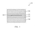
- FIG. 1 is an explanatory view schematically showing a cross section of a ceramic substrate 110.
- the ceramic substrate 110 is a low temperature co-fired ceramic (LTCC) substrate. At least a portion of a circuit for realizing a predefined function is formed on the ceramic substrate 110. In the present embodiment, a circuit for transmitting a signal to electronic components, etc. is formed in the ceramic substrate 110.
- LTCC low temperature co-fired ceramic
- the ceramic substrate 110 includes ceramic layers 121 and 122 and a conductor trace 130.
- the ceramic substrate 110 has a structure in which the plurality of ceramic layers 121 and 122 are laminated.
- the ceramic substrate 110 has unillustrated vias and unillustrated through holes in addition to the conductor trace 130 as conductors which form the circuit.
- Each of the ceramic layers 121 of the ceramic substrate 110 is a first ceramic layer which is located adjacent to the conductor trace 130.
- the ceramic layers 121 have electrically insulating properties.
- the ceramic layers 121 are mainly formed of a glass ceramic.
- "mainly formed of (a component)” means that the component accounts for at least 50 mass% of the entirety.
- each of the ceramic layers 121 is a ceramic layer which is formed by firing borosilicate glass powder and alumina (Al 2 O 3 ) powder.
- Borosilicate glass is mainly composed of silicon dioxide (SiO 2 ), alumina (Al 2 O 3 ), and boron oxide (B 2 O 3 ).
- a powder of at least one of a metal boride and a metal silicide is added to a ceramic paste which is the pre-firing form of the ceramic layer 121. Therefore, the concentration of silicon atoms (Si) and/or boron atoms (B) in the ceramic layers 121 is higher than that in the ceramic layers 122.
- each of the ceramic layers 121 has a thickness of about 10 ⁇ m.
- Each of the ceramic layers 122 of the ceramic substrate 110 is a ceramic layer which sandwiches the corresponding ceramic layer 121 in cooperation with the conductor trace 130.
- the ceramic layers 122 have electrically insulating properties.
- the ceramic layers 122 are mainly formed of a glass ceramic.
- each of the ceramic layers 122 is formed by firing borosilicate glass powder and alumina (Al 2 O 3 ) powder.
- a powder of at least one of the metal boride and the metal silicide is not added to each of green sheets which are the pre-firing form of the ceramic layers 122.
- Each of the ceramic layers 122 has a thickness sufficiently greater than that of the ceramic layers 121.
- the conductor trace 130 of the ceramic substrate 110 is mainly formed of silver (Ag).
- the conductor trace 130 contains silver (Ag) powder and borosilicate glass powder, and has electrical conductivity.
- the conductor trace 130 has a thickness of about 10 ⁇ m.
- the conductor trace 130 is sandwiched between the two ceramic layers 121 and is located adjacent to the two ceramic layers 121.
- the conductor trace 130 may be sandwiched between the ceramic layers 121 and 122 and be located adjacent to the ceramic layers 121 and 122.
- the ceramic substrate 110 may include two or more conductor traces 130 which are laminated together with other ceramic layers 121 and 122.
- FIG. 2 is a flowchart showing a method of manufacturing the ceramic substrate 110.
- a ceramic paste which is the material of each ceramic layer 121 is prepared (step P110).
- the ceramic paste which is the material of each ceramic layer 121 is a paste in which a powder of at least one of the metal boride and the metal silicide is added to a raw material powder of a glass ceramic.
- the raw material powder of the ceramic paste is prepared by mixing borosilicate glass powder and alumina powder, which are inorganic components, at a volume ratio of 60:40.
- the metal boride to be added to the ceramic paste is preferably at least one of lanthanum hexaboride (LaB 6 ), silicon hexaboride (SiB 6 ), and titanium diboride (TiB 2 ).
- the metal silicide to be added to the ceramic paste is preferably at least one of titanium disilicide (TiSi 2 ), zirconium disilicide (ZrSi 2 ), and tantalum disilicide (TaSi 2 ).
- the total amount of the metal boride and the metal silicide with respect to the amount of the inorganic component of the ceramic paste is 3 vol.% to 7 vol.% in the invention.
- a mixture of borosilicate glass powder and alumina powder, both of which are inorganic components, is prepared for producing the ceramic paste which is the material of each ceramic layer 121.
- a powder of at least one of the metal boride and the metal silicide, ethyl cellulose serving as a binder, and terpineol serving as a solvent are added to the mixture of the inorganic components.
- the resultant material is kneaded with a triple roll mill, whereby the ceramic paste is obtained.
- the ceramic paste After preparation of the ceramic paste, which is to become a ceramic layer 121 after firing (step P110), the ceramic paste is applied to a green sheet which is to become a ceramic layer 122 after firing (step P120).
- the ceramic paste is applied to the green sheet by means of screen printing.
- the green sheet which is the material of each ceramic layer 122 is prepared.
- the green sheet is formed by mixing powders of inorganic components with a binder, a plasticizer, a solvent, etc., and forming the resultant mixture into the shape of a thin plate (sheet).
- powders of borosilicate glass and alumina which are inorganic components are weighed such that their volume ratio becomes 60:40 and the total weight becomes 1 kg. These powders are placed in a container (pot) formed of alumina.
- the ceramic paste is applied to the green sheet.
- the green sheet carrying the ceramic paste applied thereto is formed into a desired shape by means of punching.
- a conductor paste which is to become the conductor trace 130 after firing is applied to the ceramic paste having been applied to the green sheet (step P130).
- the conductor paste which is to become the conductor trace 130 after firing is prepared by mixing a binder, a plasticizer, a solvent, etc. into a powder of inorganic components; i.e., a mixture of powder of silver (Ag) and powder of borosilicate glass.
- step P130 After applying the conductor paste to the green sheet (step P130), the green sheet carrying the ceramic paste and the conductor paste applied thereto is fired (step P140). Thus, the ceramic substrate 110 is complete.
- a plurality of green sheets are laminated to form a laminate before firing the green sheets.
- a green sheet carrying the ceramic paste applied thereto is placed on another green sheet carrying the ceramic paste and the conductor paste applied thereto such that the ceramic paste side of the former comes into contact with the conductor paste side of the latter, whereby the laminate is formed.
- the laminate is formed into a shape suitable for firing.
- the laminate is exposed to an atmosphere of 250°C for 10 hours for debindering.
- the laminate after debindering, the laminate is fired by being exposed to an atmosphere of 850°C for 60 minutes. After these steps, the ceramic substrate 110 is obtained.
- the ceramic paste contains the additive component(s), the concentration of silicon atoms (Si) and/or boron atoms (B) in the ceramic layers 121 is higher than that in the ceramic layers 122 depending on the amount of the additive component(s).
- FIG. 3 is a table showing the results of an evaluation test.
- samples S01 to S09 of the ceramic substrate 110 were made through use of different ceramic pastes.
- the amount of the additive in the ceramic paste which is the pre-firing form of the ceramic layer 121 is shown as the amount (volume percent) of the additive with respect to the amount of the inorganic component of the ceramic paste.
- the method of preparing the samples S01 to S08 is the same as that described with reference to FIG. 2 .
- the method of preparing the sample S09 is the same as that described with reference to FIG. 2 except that the metal boride and the metal silicide are not added to the ceramic paste.
- a cross section of each sample was observed using a scanning electron microscope (SEM) and an electron probe micro analyzer (EPMA) to measure the distance of diffusion of silver into the ceramic layers 121 and 122.
- SEM scanning electron microscope
- EPMA electron probe micro analyzer
- the concentration of silver (Ag) at the interface between the ceramic layer 121 and the conductor trace 130 was used as a reference concentration, and the distance between the interface and a position in the ceramic layers 121 and 122 at which the concentration of silver (Ag) becomes half the reference concentration was measured at 10 points.
- the average of the measured distances was obtained as a silver diffusion distance.
- the evaluation results of the samples S01 to S03 and S09 show that diffusion of silver into the ceramic layers 121 and 122 can be prevented by adding one of lanthanum hexaboride (LaB 6 ), silicon hexaboride (SiB 6 ), and titanium diboride (TiB 2 ), which are metal borides, to the ceramic paste which is the pre-firing form of the ceramic layer 121.
- LaB 6 lanthanum hexaboride
- SiB 6 silicon hexaboride
- TiB 2 titanium diboride
- the evaluation results of the samples S04 to S06 and S09 show that diffusion of silver into the ceramic layers 121 and 122 can be prevented by adding one of titanium disilicide (TiSi 2 ), zirconium disilicide (ZrSi 2 ), and tantalum disilicide (TaSi 2 ), which are metal silicides, to the ceramic paste which is the pre-firing form of the ceramic layer 121.
- TiSi 2 titanium disilicide
- ZrSi 2 zirconium disilicide
- TaSi 2 tantalum disilicide
- the evaluation results of the samples S01 to S08 show that diffusion of silver into the ceramic layers 121 and 122 can be sufficiently prevented when the total amount of the metal boride and the metal silicide with respect to the amount of the inorganic component of the ceramic paste which is the pre-firing form of the ceramic layer 121 is 3 vol.% to 7 vol.%.
- At least one of the metal boride and the metal silicide added to the ceramic paste oxidizes during firing. Therefore, diffusion of the silver component of the conductor trace 130 into the ceramic layers 121 and 122 can be prevented. As a result, it is possible to prevent problems caused by diffusion of the silver component, for example, formation of voids in the ceramic layers 121 and 122, deformation of the ceramic layers 121 and 122, or change of color of the ceramic layers 121 and 122. Thus, the quality of the ceramic substrate 110 can be improved.
- the metal boride added to the ceramic paste may be at least one of lanthanum hexaboride (LaB 6 ), silicon hexaboride (SiB 6 ), and titanium diboride (TiB 2 ). This prevents diffusion of the silver component from the conductor trace 130 into the ceramic layers 121 and 122.
- the metal silicide added to the ceramic paste may be at least one of titanium disilicide (TiSi 2 ), zirconium disilicide (ZrSi 2 ), and tantalum disilicide (TaSi 2 ). This prevents diffusion of the silver component from the conductor trace 130 into the ceramic layers 121 and 122.
- the total amount of the metal boride and the metal silicide with respect to the amount of the inorganic component of the ceramic paste is 3 vol.% to 7 vol.%, diffusion of the silver component from the conductor trace 130 into the ceramic layers 121 and 122 can be sufficiently prevented.
- the powder of at least one of the metal boride and the metal silicide is caused to adhere to the surfaces of silver (Ag) powder particles by adding the powder of at least one of the metal boride and the metal silicide to the raw material powder. This prevents diffusion of the silver component from the conductor trace 130 into the ceramic layers 121 and 122 to a greater degree.
- the ceramic slurry may be used to make a green sheet which is to become the ceramic layer 122 after firing.
- the ceramic paste which is to become the ceramic layer 121 after firing is not required to be applied to the green sheet.
- the additive component contained in the green sheet i.e., at least one of the metal boride and the metal silicide
- oxidizes during firing Therefore, diffusion of the silver component of the conductor trace 130 into the ceramic layer 122 can be prevented.
- the quality of the ceramic substrate 110 can be improved.
Landscapes
- Engineering & Computer Science (AREA)
- Microelectronics & Electronic Packaging (AREA)
- Chemical & Material Sciences (AREA)
- Manufacturing & Machinery (AREA)
- Ceramic Engineering (AREA)
- Inorganic Chemistry (AREA)
- Organic Chemistry (AREA)
- Materials Engineering (AREA)
- Dispersion Chemistry (AREA)
- Geochemistry & Mineralogy (AREA)
- General Chemical & Material Sciences (AREA)
- Life Sciences & Earth Sciences (AREA)
- Chemical Kinetics & Catalysis (AREA)
- Crystallography & Structural Chemistry (AREA)
- Structural Engineering (AREA)
- Manufacturing Of Printed Wiring (AREA)
- Parts Printed On Printed Circuit Boards (AREA)
- Production Of Multi-Layered Print Wiring Board (AREA)
- Compositions Of Oxide Ceramics (AREA)
- Non-Metallic Protective Coatings For Printed Circuits (AREA)
- Conductive Materials (AREA)
Claims (4)
- Verfahren zur Herstellung eines Keramiksubstrats (110) mit einer hauptsächlich aus einer Glaskeramik gebildeten Keramikschicht (121, 122) und einer hauptsächlich aus Silber (Ag) gebildeten Leiterbahn (130), umfassend:einen Schritt des Herstellens einer Keramikpaste, in der ein Pulver aus mindestens einem Metallborid und/oder einem Metallsilicid zu einem Rohmaterialpulver der Glaskeramik hinzugefügt wird;einen Schritt des Aufbringens der Keramikpaste auf eine grüne Folie, die nach dem Brennen die Keramikschicht werden soll;einen Schritt des Aufbringens einer Leiterpaste, die nach dem Brennen zur Leiterbahn wird, auf die auf die grüne Folie aufgebrachte Keramikpaste; undeinen Schritt des Brennens der grünen Folie, die die Keramikpaste und die darauf aufgebrachte Leiterpaste trägt,wobei das Rohmaterialpulver der Glaskeramik Borosilikatglaspulver und Aluminiumoxidpulver (Al2O3) umfasst,wobei beim Brennen der die Keramikpaste und die darauf aufgebrachte Leiterpaste tragenden grüne Folie Sauerstoff in der Nähe der Leiterpaste durch Oxidation von mindestens einem der in der Keramikpaste enthaltenen Metallboride und Metallsilicide verbraucht wird, so dass die Oxidation der in der Leiterpaste enthaltenen Silberkomponente verhindert wird, undwobei die Gesamtmenge des Metallborids und des Metallsilizids in Bezug auf die Menge der anorganischen Komponente der Keramikpaste 3 Vol. % bis 7 Vol. % beträgt, so dass die Diffusion der Silberkomponente von der Leiterbahn in die Keramikschichten ausreichend verhindert werden kann.
- Verfahren zur Herstellung eines Keramiksubstrats (110) nach Anspruch 1, wobei das Metallborid mindestens eines von Lanthanhexaborid (LaB6), Siliziumhexaborid (SiB6) und Titandiborid (TiB2) ist.
- Verfahren zur Herstellung eines Keramiksubstrats (110) nach Anspruch 1 oder 2, wobei das Metallsilicid mindestens eines von Titandisilicid (TiSi2), Zirkoniumdisilicid (ZrSi2) und Tantaldisilicid (TaSi2) ist.
- Verfahren zur Herstellung eines Keramiksubstrats (110) mit einer hauptsächlich aus einer Glaskeramik gebildeten Keramikschicht (121, 122) und einer hauptsächlich aus Silber (Ag) gebildeten Leiterbahn (130), umfassend:einen Schritt des Herstellens einer Keramikaufschlämmung, in der ein Pulver aus mindestens einem Metallborid und/oder einem Metallsilicid zu einem Rohmaterialpulver der Glaskeramik hinzugefügt wird;einen Schritt des Herstellens einer grünen Folie aus der Keramikaufschlämmung, die nach dem Brennen die Keramikschicht werden soll;einen Schritt des Aufbringens einer Leiterpaste, die nach dem Brennen die Leiterbahn werden soll, auf die grüne Folie; undeinen Schritt des Brennens der grünen Folie, die die darauf aufgebrachte Leiterpaste trägt,wobei das Rohmaterialpulver der Glaskeramik Borosilikatglaspulver und Aluminiumoxidpulver (Al2O3) umfasst,wobei beim Brennen der grünen Folie, die die darauf aufgebrachte Leiterpaste trägt, Sauerstoff in der Nähe der Leiterpaste durch Oxidation von mindestens einem der in der grünen Folie enthaltenen Metallboride und Metallsilicide verbraucht wird, so dass die Oxidation der in der Leiterpaste enthaltenen Silberkomponente verhindert wird, undwobei die Gesamtmenge des Metallborids und des Metallsilizids in Bezug auf die Menge der anorganischen Komponente in der grünen Folie 3 Vol. % bis 7 Vol. % beträgt, so dass die Diffusion der Silberkomponente von der Leiterbahn in die Keramikschichten ausreichend verhindert werden kann.
Applications Claiming Priority (2)
| Application Number | Priority Date | Filing Date | Title |
|---|---|---|---|
| JP2015003819 | 2015-01-13 | ||
| PCT/JP2016/000080 WO2016114119A1 (ja) | 2015-01-13 | 2016-01-08 | セラミック基板およびその製造方法 |
Publications (3)
| Publication Number | Publication Date |
|---|---|
| EP3247184A1 EP3247184A1 (de) | 2017-11-22 |
| EP3247184A4 EP3247184A4 (de) | 2018-08-29 |
| EP3247184B1 true EP3247184B1 (de) | 2025-03-12 |
Family
ID=56405670
Family Applications (4)
| Application Number | Title | Priority Date | Filing Date |
|---|---|---|---|
| EP16737189.7A Active EP3247181B1 (de) | 2015-01-13 | 2016-01-08 | Herstellungsverfahren für eine leiterplatte |
| EP16737190.5A Active EP3247184B1 (de) | 2015-01-13 | 2016-01-08 | Herstellungsverfahren für ein keramiksubstrat |
| EP16737192.1A Pending EP3247182A4 (de) | 2015-01-13 | 2016-01-08 | Verfahren zur herstellung von keramiksubstraten, keramiksubstrat und silberbasiertes leitfähiges material |
| EP16737191.3A Active EP3247180B1 (de) | 2015-01-13 | 2016-01-08 | Keramisches substrat |
Family Applications Before (1)
| Application Number | Title | Priority Date | Filing Date |
|---|---|---|---|
| EP16737189.7A Active EP3247181B1 (de) | 2015-01-13 | 2016-01-08 | Herstellungsverfahren für eine leiterplatte |
Family Applications After (2)
| Application Number | Title | Priority Date | Filing Date |
|---|---|---|---|
| EP16737192.1A Pending EP3247182A4 (de) | 2015-01-13 | 2016-01-08 | Verfahren zur herstellung von keramiksubstraten, keramiksubstrat und silberbasiertes leitfähiges material |
| EP16737191.3A Active EP3247180B1 (de) | 2015-01-13 | 2016-01-08 | Keramisches substrat |
Country Status (6)
| Country | Link |
|---|---|
| US (5) | US20180035549A1 (de) |
| EP (4) | EP3247181B1 (de) |
| JP (4) | JP6309631B2 (de) |
| KR (4) | KR101994566B1 (de) |
| CN (4) | CN107113969B (de) |
| WO (4) | WO2016114119A1 (de) |
Families Citing this family (9)
| Publication number | Priority date | Publication date | Assignee | Title |
|---|---|---|---|---|
| EP3247181B1 (de) * | 2015-01-13 | 2025-02-19 | Niterra Co., Ltd. | Herstellungsverfahren für eine leiterplatte |
| CN110255912A (zh) * | 2019-07-03 | 2019-09-20 | 东北大学秦皇岛分校 | 一种微晶玻璃工艺品的制作方法 |
| CN111312427B (zh) * | 2020-04-17 | 2021-08-31 | 洛阳理工学院 | 一种用于低温共烧低介电常数介质陶瓷的多层布线用银浆 |
| CN112225547B (zh) * | 2020-10-19 | 2022-04-19 | 上海晶材新材料科技有限公司 | Ltcc材料、基板及制备方法 |
| CN112235959A (zh) * | 2020-10-28 | 2021-01-15 | 上海读家电子科技有限公司 | 可加强铂钯银导体抗银迁移能力的陶瓷电路板制造方法 |
| CN112216655A (zh) * | 2020-11-03 | 2021-01-12 | 中国电子科技集团公司第四十三研究所 | 一种LTCC基SiP封装外壳及其制备方法 |
| US20220367363A1 (en) * | 2021-05-17 | 2022-11-17 | Onano Industrial Corp. | Ltcc electronic device unit structure |
| CN113690033A (zh) * | 2021-07-23 | 2021-11-23 | 东莞市优琥电子科技有限公司 | 变压器和电源适配器 |
| US20230307314A1 (en) * | 2022-03-24 | 2023-09-28 | Texas Instruments Incorporated | Direct bond copper substrate with metal filled ceramic substrate indentations |
Family Cites Families (55)
| Publication number | Priority date | Publication date | Assignee | Title |
|---|---|---|---|---|
| JPS6029240B2 (ja) * | 1977-12-02 | 1985-07-09 | 富士通株式会社 | セラミック回路基板の製法 |
| JPS5491790A (en) * | 1977-12-29 | 1979-07-20 | Junkosha Co Ltd | Flat cable |
| US4279654A (en) * | 1979-05-14 | 1981-07-21 | The Foundation: The Research Institute For Special Inorganic Materials | Process for production of crystallized glass and process for producing composite article using said crystallized glass |
| JPS61168564A (ja) * | 1985-01-18 | 1986-07-30 | 株式会社日立製作所 | セラミツク絶縁基板 |
| US4639391A (en) * | 1985-03-14 | 1987-01-27 | Cts Corporation | Thick film resistive paint and resistors made therefrom |
| DE3621667A1 (de) * | 1985-06-29 | 1987-01-08 | Toshiba Kawasaki Kk | Mit einer mehrzahl von dickfilmen beschichtetes substrat, verfahren zu seiner herstellung und dieses enthaltende vorrichtung |
| US4777014A (en) * | 1986-03-07 | 1988-10-11 | Lanxide Technology Company, Lp | Process for preparing self-supporting bodies and products made thereby |
| JPH0619926B2 (ja) | 1987-11-11 | 1994-03-16 | 株式会社日立製作所 | 回路基板とその製法 |
| DE3935471A1 (de) * | 1989-10-25 | 1991-05-02 | Hoechst Ag | Keramische stoffzusammensetzung und ihre verwendung |
| JPH03233831A (ja) * | 1990-02-07 | 1991-10-17 | Dai Ichi Kogyo Seiyaku Co Ltd | 6ホウ化ランタン含有ペースト |
| JPH0719964B2 (ja) * | 1990-08-08 | 1995-03-06 | 日本電気株式会社 | 銀系配線セラミック基板 |
| JPH04314394A (ja) * | 1991-04-12 | 1992-11-05 | Fujitsu Ltd | ガラスセラミック回路基板とその製造方法 |
| JPH0793228B2 (ja) * | 1991-04-24 | 1995-10-09 | 太陽誘電株式会社 | 希土類入り銀導電ペーストおよびこれを用いた電子部品 |
| JP2985503B2 (ja) | 1992-04-22 | 1999-12-06 | 株式会社村田製作所 | 導電ペースト組成物 |
| JPH0595071U (ja) * | 1992-05-28 | 1993-12-24 | 京セラ株式会社 | 厚膜回路基板 |
| EP0575813B1 (de) * | 1992-06-08 | 1996-12-27 | NEC Corporation | Glaskeramisches Mehrschichtsubstrat und Verfahren zur seiner Herstellung |
| JP3448747B2 (ja) * | 1992-08-25 | 2003-09-22 | 松下電器産業株式会社 | 多層セラミック基板の製造方法 |
| DE4345586B4 (de) * | 1992-12-22 | 2009-04-23 | Denso Corp., Kariya-shi | Verfahren zum Erzeugen von Vielfach-Dickschichtsubstraten |
| JPH06204511A (ja) * | 1993-01-07 | 1994-07-22 | Dai Ichi Kogyo Seiyaku Co Ltd | 半導体基板用電極ペースト |
| JPH06252524A (ja) * | 1993-02-26 | 1994-09-09 | Asahi Glass Co Ltd | 導体付きセラミックス基板の製造方法 |
| JPH07135394A (ja) * | 1993-11-09 | 1995-05-23 | Ngk Spark Plug Co Ltd | 厚膜コンデンサ付きセラミック配線基板及びその製造方法 |
| US5474619A (en) * | 1994-05-04 | 1995-12-12 | The United States Of America As Represented By The Secretary Of Commerce | Thin film high temperature silicide thermocouples |
| JPH08259331A (ja) * | 1995-03-22 | 1996-10-08 | Agency Of Ind Science & Technol | 可塑成形用窒化ケイ素−水系組成物の調製法 |
| JPH08298382A (ja) * | 1995-04-26 | 1996-11-12 | Tdk Corp | セラミックス多層基板 |
| JP3927250B2 (ja) * | 1995-08-16 | 2007-06-06 | イー・アイ・デュポン・ドウ・ヌムール・アンド・カンパニー | 窒化アルミニウム基板用厚膜導体ペースト組成物 |
| JPH09246722A (ja) * | 1996-03-08 | 1997-09-19 | Sumitomo Metal Ind Ltd | ガラスセラミックス多層配線基板とその製造方法 |
| US5857253A (en) * | 1996-03-20 | 1999-01-12 | Ppg Industries, Inc. | System and methods for forming bushing plates |
| JP4099837B2 (ja) * | 1997-08-27 | 2008-06-11 | 株式会社村田製作所 | 低温焼成セラミック多層基板の製造方法 |
| JPH11339560A (ja) * | 1998-05-29 | 1999-12-10 | Murata Mfg Co Ltd | 銀ペースト |
| JP2001278657A (ja) * | 2000-01-24 | 2001-10-10 | Ngk Spark Plug Co Ltd | 低温焼成磁器組成物及びその製造方法並びにその低温焼成磁器組成物を用いた低温焼成配線基板 |
| CA2478142C (en) * | 2001-03-09 | 2009-09-15 | Datec Coating Corporation | Sol-gel derived resistive and conductive coating |
| JP3636123B2 (ja) * | 2001-09-20 | 2005-04-06 | 株式会社村田製作所 | 積層セラミック電子部品の製造方法、および積層セラミック電子部品 |
| ATE334949T1 (de) * | 2001-10-09 | 2006-08-15 | Du Pont | Dickfilm-leiterzusammensetzungen zur verwendung auf alumniumnitridsubstraten |
| JP2003268567A (ja) * | 2002-03-19 | 2003-09-25 | Hitachi Cable Ltd | 導電材被覆耐食性金属材料 |
| JP3988533B2 (ja) * | 2002-05-23 | 2007-10-10 | 株式会社村田製作所 | ガラスセラミック組成物、ガラスセラミック、およびセラミック多層基板 |
| US7323805B2 (en) * | 2004-01-28 | 2008-01-29 | Kabushiki Kaisha Toshiba | Piezoelectric thin film device and method for manufacturing the same |
| US7218506B2 (en) * | 2004-03-31 | 2007-05-15 | Tdk Corporation | Electrolytic capacitor and method of manufacturing the same |
| JP2006073280A (ja) * | 2004-08-31 | 2006-03-16 | Ngk Spark Plug Co Ltd | メタライズ組成物及びセラミック配線基板 |
| JP4548050B2 (ja) * | 2004-09-03 | 2010-09-22 | 株式会社村田製作所 | セラミック多層基板 |
| JP2006253600A (ja) * | 2005-03-14 | 2006-09-21 | Ngk Spark Plug Co Ltd | 配線基板の製造方法 |
| KR100657321B1 (ko) * | 2005-06-30 | 2006-12-14 | 삼성전자주식회사 | 인쇄데이터 관리방법 및 장치 |
| TW200710882A (en) * | 2005-07-28 | 2007-03-16 | Du Pont | Conductor composition for use in LTCC photosensitive tape on substrate applications |
| US20070023388A1 (en) | 2005-07-28 | 2007-02-01 | Nair Kumaran M | Conductor composition for use in LTCC photosensitive tape on substrate applications |
| JP4797534B2 (ja) | 2005-09-16 | 2011-10-19 | Tdk株式会社 | 多層セラミックス基板 |
| US7666328B2 (en) * | 2005-11-22 | 2010-02-23 | E. I. Du Pont De Nemours And Company | Thick film conductor composition(s) and processing technology thereof for use in multilayer electronic circuits and devices |
| JP4867399B2 (ja) | 2006-03-03 | 2012-02-01 | 旭硝子株式会社 | 導体ペーストおよびセラミック多層基板製造方法 |
| JP4967388B2 (ja) * | 2006-03-15 | 2012-07-04 | パナソニック株式会社 | セラミック積層デバイスの製造方法およびセラミック積層デバイス |
| KR100956219B1 (ko) * | 2008-02-25 | 2010-05-04 | 삼성전기주식회사 | 확산 방지층을 갖는 저온동시소성 세라믹 기판 및 그 제조방법 |
| JPWO2011102040A1 (ja) * | 2010-02-19 | 2013-06-17 | 旭硝子株式会社 | 素子搭載用基板およびその製造方法 |
| JP5488282B2 (ja) | 2010-07-13 | 2014-05-14 | 昭栄化学工業株式会社 | 導電性ペースト |
| JP5949770B2 (ja) * | 2011-08-09 | 2016-07-13 | 旭硝子株式会社 | ガラスセラミックス体、発光素子搭載用基板、および発光装置 |
| JP2013153051A (ja) * | 2012-01-25 | 2013-08-08 | Tokuyama Corp | メタライズドセラミックスビア基板及びその製造方法 |
| GB2504957A (en) * | 2012-08-14 | 2014-02-19 | Henkel Ag & Co Kgaa | Curable compositions comprising composite particles |
| JP2014179473A (ja) | 2013-03-15 | 2014-09-25 | Ngk Spark Plug Co Ltd | セラミック基板の製造方法および導体材料 |
| EP3247181B1 (de) * | 2015-01-13 | 2025-02-19 | Niterra Co., Ltd. | Herstellungsverfahren für eine leiterplatte |
-
2016
- 2016-01-08 EP EP16737189.7A patent/EP3247181B1/de active Active
- 2016-01-08 US US15/543,253 patent/US20180035549A1/en not_active Abandoned
- 2016-01-08 JP JP2016541726A patent/JP6309631B2/ja active Active
- 2016-01-08 US US15/543,290 patent/US20180014408A1/en not_active Abandoned
- 2016-01-08 US US15/543,264 patent/US10375837B2/en active Active
- 2016-01-08 WO PCT/JP2016/000080 patent/WO2016114119A1/ja not_active Ceased
- 2016-01-08 CN CN201680005732.7A patent/CN107113969B/zh active Active
- 2016-01-08 EP EP16737190.5A patent/EP3247184B1/de active Active
- 2016-01-08 KR KR1020177019496A patent/KR101994566B1/ko active Active
- 2016-01-08 KR KR1020177019497A patent/KR102017401B1/ko active Active
- 2016-01-08 US US15/542,871 patent/US10524365B2/en active Active
- 2016-01-08 KR KR1020177019498A patent/KR102059318B1/ko active Active
- 2016-01-08 CN CN201680005796.7A patent/CN107113976B/zh active Active
- 2016-01-08 CN CN201680005805.2A patent/CN107113986B/zh active Active
- 2016-01-08 KR KR1020177019495A patent/KR102028896B1/ko active Active
- 2016-01-08 EP EP16737192.1A patent/EP3247182A4/de active Pending
- 2016-01-08 WO PCT/JP2016/000079 patent/WO2016114118A1/ja not_active Ceased
- 2016-01-08 WO PCT/JP2016/000081 patent/WO2016114120A1/ja not_active Ceased
- 2016-01-08 JP JP2016542286A patent/JP6309632B2/ja active Active
- 2016-01-08 JP JP2016541735A patent/JP6553048B2/ja active Active
- 2016-01-08 CN CN201680005790.XA patent/CN107211535B/zh active Active
- 2016-01-08 JP JP2016541738A patent/JP6261746B2/ja active Active
- 2016-01-08 WO PCT/JP2016/000082 patent/WO2016114121A1/ja not_active Ceased
- 2016-01-08 EP EP16737191.3A patent/EP3247180B1/de active Active
-
2018
- 2018-07-10 US US16/031,828 patent/US10785879B2/en active Active
Also Published As
Similar Documents
| Publication | Publication Date | Title |
|---|---|---|
| EP3247184B1 (de) | Herstellungsverfahren für ein keramiksubstrat | |
| JP2012164784A (ja) | 積層セラミック電子部品 | |
| WO2001056047A1 (fr) | Reseau conducteur integre a une carte multicouche, carte multicouche a reseau conducteur integre et procede de fabrication de carte multicouche | |
| JPH1192256A (ja) | 無機基板用導体、導体用ペースト及びこれを用いた無機多層基板 | |
| JP2002128581A (ja) | 銅メタライズ組成物ならびにそれを用いたセラミック配線基板およびその製造方法 | |
| JP2010258175A (ja) | セラミック基板の製造方法 | |
| JP2008037675A (ja) | 低温焼結セラミック組成物、セラミック基板およびその製造方法、ならびに電子部品 | |
| JP2002232146A (ja) | ビアホール導体用組成物ならびに多層セラミック基板およびその製造方法 |
Legal Events
| Date | Code | Title | Description |
|---|---|---|---|
| STAA | Information on the status of an ep patent application or granted ep patent |
Free format text: STATUS: THE INTERNATIONAL PUBLICATION HAS BEEN MADE |
|
| PUAI | Public reference made under article 153(3) epc to a published international application that has entered the european phase |
Free format text: ORIGINAL CODE: 0009012 |
|
| STAA | Information on the status of an ep patent application or granted ep patent |
Free format text: STATUS: REQUEST FOR EXAMINATION WAS MADE |
|
| 17P | Request for examination filed |
Effective date: 20170713 |
|
| AK | Designated contracting states |
Kind code of ref document: A1 Designated state(s): AL AT BE BG CH CY CZ DE DK EE ES FI FR GB GR HR HU IE IS IT LI LT LU LV MC MK MT NL NO PL PT RO RS SE SI SK SM TR |
|
| AX | Request for extension of the european patent |
Extension state: BA ME |
|
| DAV | Request for validation of the european patent (deleted) | ||
| DAX | Request for extension of the european patent (deleted) | ||
| A4 | Supplementary search report drawn up and despatched |
Effective date: 20180727 |
|
| RIC1 | Information provided on ipc code assigned before grant |
Ipc: H05K 1/03 20060101ALI20180723BHEP Ipc: H05K 3/46 20060101AFI20180723BHEP |
|
| STAA | Information on the status of an ep patent application or granted ep patent |
Free format text: STATUS: EXAMINATION IS IN PROGRESS |
|
| 17Q | First examination report despatched |
Effective date: 20210415 |
|
| RAP3 | Party data changed (applicant data changed or rights of an application transferred) |
Owner name: NITERRA CO., LTD. |
|
| REG | Reference to a national code |
Ref country code: DE Ref legal event code: R079 Free format text: PREVIOUS MAIN CLASS: H05K0003460000 Ipc: H05K0001030000 Ref country code: DE Ref legal event code: R079 Ref document number: 602016091514 Country of ref document: DE Free format text: PREVIOUS MAIN CLASS: H05K0003460000 Ipc: H05K0001030000 |
|
| GRAP | Despatch of communication of intention to grant a patent |
Free format text: ORIGINAL CODE: EPIDOSNIGR1 |
|
| STAA | Information on the status of an ep patent application or granted ep patent |
Free format text: STATUS: GRANT OF PATENT IS INTENDED |
|
| RIC1 | Information provided on ipc code assigned before grant |
Ipc: H05K 3/28 20060101ALI20241022BHEP Ipc: H05K 3/12 20060101ALI20241022BHEP Ipc: H05K 1/09 20060101ALI20241022BHEP Ipc: H05K 3/46 20060101ALI20241022BHEP Ipc: H05K 1/03 20060101AFI20241022BHEP |
|
| INTG | Intention to grant announced |
Effective date: 20241111 |
|
| GRAS | Grant fee paid |
Free format text: ORIGINAL CODE: EPIDOSNIGR3 |
|
| GRAA | (expected) grant |
Free format text: ORIGINAL CODE: 0009210 |
|
| STAA | Information on the status of an ep patent application or granted ep patent |
Free format text: STATUS: THE PATENT HAS BEEN GRANTED |
|
| AK | Designated contracting states |
Kind code of ref document: B1 Designated state(s): AL AT BE BG CH CY CZ DE DK EE ES FI FR GB GR HR HU IE IS IT LI LT LU LV MC MK MT NL NO PL PT RO RS SE SI SK SM TR |
|
| REG | Reference to a national code |
Ref country code: GB Ref legal event code: FG4D |
|
| REG | Reference to a national code |
Ref country code: CH Ref legal event code: EP |
|
| REG | Reference to a national code |
Ref country code: DE Ref legal event code: R096 Ref document number: 602016091514 Country of ref document: DE |
|
| REG | Reference to a national code |
Ref country code: IE Ref legal event code: FG4D |
|
| PG25 | Lapsed in a contracting state [announced via postgrant information from national office to epo] |
Ref country code: RS Free format text: LAPSE BECAUSE OF FAILURE TO SUBMIT A TRANSLATION OF THE DESCRIPTION OR TO PAY THE FEE WITHIN THE PRESCRIBED TIME-LIMIT Effective date: 20250612 |
|
| PG25 | Lapsed in a contracting state [announced via postgrant information from national office to epo] |
Ref country code: FI Free format text: LAPSE BECAUSE OF FAILURE TO SUBMIT A TRANSLATION OF THE DESCRIPTION OR TO PAY THE FEE WITHIN THE PRESCRIBED TIME-LIMIT Effective date: 20250312 |
|
| PG25 | Lapsed in a contracting state [announced via postgrant information from national office to epo] |
Ref country code: ES Free format text: LAPSE BECAUSE OF FAILURE TO SUBMIT A TRANSLATION OF THE DESCRIPTION OR TO PAY THE FEE WITHIN THE PRESCRIBED TIME-LIMIT Effective date: 20250312 |
|
| REG | Reference to a national code |
Ref country code: LT Ref legal event code: MG9D |
|
| PG25 | Lapsed in a contracting state [announced via postgrant information from national office to epo] |
Ref country code: NO Free format text: LAPSE BECAUSE OF FAILURE TO SUBMIT A TRANSLATION OF THE DESCRIPTION OR TO PAY THE FEE WITHIN THE PRESCRIBED TIME-LIMIT Effective date: 20250612 |
|
| PG25 | Lapsed in a contracting state [announced via postgrant information from national office to epo] |
Ref country code: HR Free format text: LAPSE BECAUSE OF FAILURE TO SUBMIT A TRANSLATION OF THE DESCRIPTION OR TO PAY THE FEE WITHIN THE PRESCRIBED TIME-LIMIT Effective date: 20250312 |
|
| REG | Reference to a national code |
Ref country code: NL Ref legal event code: MP Effective date: 20250312 |
|
| PG25 | Lapsed in a contracting state [announced via postgrant information from national office to epo] |
Ref country code: LV Free format text: LAPSE BECAUSE OF FAILURE TO SUBMIT A TRANSLATION OF THE DESCRIPTION OR TO PAY THE FEE WITHIN THE PRESCRIBED TIME-LIMIT Effective date: 20250312 |
|
| PG25 | Lapsed in a contracting state [announced via postgrant information from national office to epo] |
Ref country code: GR Free format text: LAPSE BECAUSE OF FAILURE TO SUBMIT A TRANSLATION OF THE DESCRIPTION OR TO PAY THE FEE WITHIN THE PRESCRIBED TIME-LIMIT Effective date: 20250613 Ref country code: BG Free format text: LAPSE BECAUSE OF FAILURE TO SUBMIT A TRANSLATION OF THE DESCRIPTION OR TO PAY THE FEE WITHIN THE PRESCRIBED TIME-LIMIT Effective date: 20250312 |
|
| PG25 | Lapsed in a contracting state [announced via postgrant information from national office to epo] |
Ref country code: NL Free format text: LAPSE BECAUSE OF FAILURE TO SUBMIT A TRANSLATION OF THE DESCRIPTION OR TO PAY THE FEE WITHIN THE PRESCRIBED TIME-LIMIT Effective date: 20250312 |
|
| PG25 | Lapsed in a contracting state [announced via postgrant information from national office to epo] |
Ref country code: SE Free format text: LAPSE BECAUSE OF FAILURE TO SUBMIT A TRANSLATION OF THE DESCRIPTION OR TO PAY THE FEE WITHIN THE PRESCRIBED TIME-LIMIT Effective date: 20250312 |
|
| PG25 | Lapsed in a contracting state [announced via postgrant information from national office to epo] |
Ref country code: SM Free format text: LAPSE BECAUSE OF FAILURE TO SUBMIT A TRANSLATION OF THE DESCRIPTION OR TO PAY THE FEE WITHIN THE PRESCRIBED TIME-LIMIT Effective date: 20250312 |
|
| PG25 | Lapsed in a contracting state [announced via postgrant information from national office to epo] |
Ref country code: PT Free format text: LAPSE BECAUSE OF FAILURE TO SUBMIT A TRANSLATION OF THE DESCRIPTION OR TO PAY THE FEE WITHIN THE PRESCRIBED TIME-LIMIT Effective date: 20250714 |
|
| PG25 | Lapsed in a contracting state [announced via postgrant information from national office to epo] |
Ref country code: IT Free format text: LAPSE BECAUSE OF FAILURE TO SUBMIT A TRANSLATION OF THE DESCRIPTION OR TO PAY THE FEE WITHIN THE PRESCRIBED TIME-LIMIT Effective date: 20250312 Ref country code: PL Free format text: LAPSE BECAUSE OF FAILURE TO SUBMIT A TRANSLATION OF THE DESCRIPTION OR TO PAY THE FEE WITHIN THE PRESCRIBED TIME-LIMIT Effective date: 20250312 |
|
| PG25 | Lapsed in a contracting state [announced via postgrant information from national office to epo] |
Ref country code: CZ Free format text: LAPSE BECAUSE OF FAILURE TO SUBMIT A TRANSLATION OF THE DESCRIPTION OR TO PAY THE FEE WITHIN THE PRESCRIBED TIME-LIMIT Effective date: 20250312 Ref country code: EE Free format text: LAPSE BECAUSE OF FAILURE TO SUBMIT A TRANSLATION OF THE DESCRIPTION OR TO PAY THE FEE WITHIN THE PRESCRIBED TIME-LIMIT Effective date: 20250312 |
|
| PG25 | Lapsed in a contracting state [announced via postgrant information from national office to epo] |
Ref country code: RO Free format text: LAPSE BECAUSE OF FAILURE TO SUBMIT A TRANSLATION OF THE DESCRIPTION OR TO PAY THE FEE WITHIN THE PRESCRIBED TIME-LIMIT Effective date: 20250312 |
|
| PG25 | Lapsed in a contracting state [announced via postgrant information from national office to epo] |
Ref country code: SK Free format text: LAPSE BECAUSE OF FAILURE TO SUBMIT A TRANSLATION OF THE DESCRIPTION OR TO PAY THE FEE WITHIN THE PRESCRIBED TIME-LIMIT Effective date: 20250312 |
|
| PG25 | Lapsed in a contracting state [announced via postgrant information from national office to epo] |
Ref country code: IS Free format text: LAPSE BECAUSE OF FAILURE TO SUBMIT A TRANSLATION OF THE DESCRIPTION OR TO PAY THE FEE WITHIN THE PRESCRIBED TIME-LIMIT Effective date: 20250712 |
|
| REG | Reference to a national code |
Ref country code: DE Ref legal event code: R097 Ref document number: 602016091514 Country of ref document: DE |
|
| PG25 | Lapsed in a contracting state [announced via postgrant information from national office to epo] |
Ref country code: DK Free format text: LAPSE BECAUSE OF FAILURE TO SUBMIT A TRANSLATION OF THE DESCRIPTION OR TO PAY THE FEE WITHIN THE PRESCRIBED TIME-LIMIT Effective date: 20250312 |
|
| PGFP | Annual fee paid to national office [announced via postgrant information from national office to epo] |
Ref country code: BE Payment date: 20251223 Year of fee payment: 11 |
|
| PLBE | No opposition filed within time limit |
Free format text: ORIGINAL CODE: 0009261 |
|
| STAA | Information on the status of an ep patent application or granted ep patent |
Free format text: STATUS: NO OPPOSITION FILED WITHIN TIME LIMIT |
|
| REG | Reference to a national code |
Ref country code: CH Ref legal event code: L10 Free format text: ST27 STATUS EVENT CODE: U-0-0-L10-L00 (AS PROVIDED BY THE NATIONAL OFFICE) Effective date: 20260121 |
|
| 26N | No opposition filed |
Effective date: 20251215 |
|
| REG | Reference to a national code |
Ref country code: AT Ref legal event code: UEP Ref document number: 1776101 Country of ref document: AT Kind code of ref document: T Effective date: 20250312 |
|
| PGFP | Annual fee paid to national office [announced via postgrant information from national office to epo] |
Ref country code: DE Payment date: 20251203 Year of fee payment: 11 |
|
| PGFP | Annual fee paid to national office [announced via postgrant information from national office to epo] |
Ref country code: AT Payment date: 20251230 Year of fee payment: 11 |