EP3879706A1 - Dispositif de réseau prédiffusé programmable par l'utilisateur - Google Patents
Dispositif de réseau prédiffusé programmable par l'utilisateur Download PDFInfo
- Publication number
- EP3879706A1 EP3879706A1 EP20163052.2A EP20163052A EP3879706A1 EP 3879706 A1 EP3879706 A1 EP 3879706A1 EP 20163052 A EP20163052 A EP 20163052A EP 3879706 A1 EP3879706 A1 EP 3879706A1
- Authority
- EP
- European Patent Office
- Prior art keywords
- layer structure
- fpga device
- clb
- hemt
- fpga
- Prior art date
- Legal status (The legal status is an assumption and is not a legal conclusion. Google has not performed a legal analysis and makes no representation as to the accuracy of the status listed.)
- Withdrawn
Links
Images

Classifications
-
- H—ELECTRICITY
- H03—ELECTRONIC CIRCUITRY
- H03K—PULSE TECHNIQUE
- H03K19/00—Logic circuits, i.e. having at least two inputs acting on one output; Inverting circuits
- H03K19/02—Logic circuits, i.e. having at least two inputs acting on one output; Inverting circuits using specified components
- H03K19/173—Logic circuits, i.e. having at least two inputs acting on one output; Inverting circuits using specified components using elementary logic circuits as components
- H03K19/177—Logic circuits, i.e. having at least two inputs acting on one output; Inverting circuits using specified components using elementary logic circuits as components arranged in matrix form
- H03K19/17724—Structural details of logic blocks
- H03K19/17728—Reconfigurable logic blocks, e.g. lookup tables
-
- H—ELECTRICITY
- H03—ELECTRONIC CIRCUITRY
- H03K—PULSE TECHNIQUE
- H03K19/00—Logic circuits, i.e. having at least two inputs acting on one output; Inverting circuits
- H03K19/02—Logic circuits, i.e. having at least two inputs acting on one output; Inverting circuits using specified components
- H03K19/173—Logic circuits, i.e. having at least two inputs acting on one output; Inverting circuits using specified components using elementary logic circuits as components
- H03K19/177—Logic circuits, i.e. having at least two inputs acting on one output; Inverting circuits using specified components using elementary logic circuits as components arranged in matrix form
- H03K19/17736—Structural details of routing resources
- H03K19/17744—Structural details of routing resources for input/output signals
-
- H—ELECTRICITY
- H03—ELECTRONIC CIRCUITRY
- H03K—PULSE TECHNIQUE
- H03K19/00—Logic circuits, i.e. having at least two inputs acting on one output; Inverting circuits
- H03K19/02—Logic circuits, i.e. having at least two inputs acting on one output; Inverting circuits using specified components
- H03K19/173—Logic circuits, i.e. having at least two inputs acting on one output; Inverting circuits using specified components using elementary logic circuits as components
- H03K19/177—Logic circuits, i.e. having at least two inputs acting on one output; Inverting circuits using specified components using elementary logic circuits as components arranged in matrix form
- H03K19/17748—Structural details of configuration resources
- H03K19/1776—Structural details of configuration resources for memories
-
- H—ELECTRICITY
- H10—SEMICONDUCTOR DEVICES; ELECTRIC SOLID-STATE DEVICES NOT OTHERWISE PROVIDED FOR
- H10D—INORGANIC ELECTRIC SEMICONDUCTOR DEVICES
- H10D84/00—Integrated devices formed in or on semiconductor substrates that comprise only semiconducting layers, e.g. on Si wafers or on GaAs-on-Si wafers
- H10D84/01—Manufacture or treatment
- H10D84/02—Manufacture or treatment characterised by using material-based technologies
- H10D84/05—Manufacture or treatment characterised by using material-based technologies using Group III-V technology
-
- H—ELECTRICITY
- H10—SEMICONDUCTOR DEVICES; ELECTRIC SOLID-STATE DEVICES NOT OTHERWISE PROVIDED FOR
- H10D—INORGANIC ELECTRIC SEMICONDUCTOR DEVICES
- H10D84/00—Integrated devices formed in or on semiconductor substrates that comprise only semiconducting layers, e.g. on Si wafers or on GaAs-on-Si wafers
- H10D84/80—Integrated devices formed in or on semiconductor substrates that comprise only semiconducting layers, e.g. on Si wafers or on GaAs-on-Si wafers characterised by the integration of at least one component covered by groups H10D12/00 or H10D30/00, e.g. integration of IGFETs
- H10D84/811—Combinations of field-effect devices and one or more diodes, capacitors or resistors
- H10D84/817—Combinations of field-effect devices and resistors only
Definitions
- the present invention relates to field-programmable gate array, FPGA, devices.
- the invention relates to artificial intelligence, Al, accelerator FPGA devices and other hardware for performing autonomous driving calculations.
- FPGAs Field-programmable gate arrays
- ASICs application-specific integrated circuits
- SoC system-on-a-chip
- FPGAs are versatile components comprising large amounts of configurable logic and are a natural choice for building and testing the new integrated circuits, ICs.
- ICs As IC designs have grown in both size and complexity, FPGAs have also grown to provide ever-increasing and corresponding numbers of logical gates.
- FPGA prototypes enables development and testing of systems more flexibly and may grant software developers earlier access to more functionally advanced hardware platforms.
- FPGAs may be used in artificial intelligence, Al, accelerators that typically need to perform very large volumes of calculations.
- FPGAs For autonomous driving applications, especially when relying on stored electrical energy for propulsion as in an electric vehicle, EV, this may become an issue as FPGAs generally consume more power than ASICs.
- Typical figures for AI accelerator FPGA power consumption may be in the range 1-5 kW.
- an autonomous EVs range could be substantially reduced, e.g. by 5-10%.
- the higher power consumption may be attributed to more logical gates and more wiring between logical gates being required in an FPGA.
- the higher power consumption may additionally lead to larger thermal losses. Increases in temperature may additionally cause thermal runway effects as current leakage increases through the conventional Si transistors, commonly used in FPGAs. There is thus need for improvements within the technical field.
- An object of the inventor has been to solve or at least mitigate some of the above issues in the state of the art.
- a field-programmable gate array, FPGA, device may be an artificial intelligence, AI, accelerator FPGA device.
- the FPGA device may be configured for, or suitable for, performing autonomous driving calculations.
- the FPGA device comprises a configurable logic block, CLB.
- the CLB comprises one logic inverter.
- the logic inverter comprises at least one high-electron-mobility transistor, HEMT.
- Each HEMT comprises an Al y Ga y-1 N layer structure, wherein 0 ⁇ y ⁇ 1, and a GaN layer structure.
- field-programmable gate array device (and its corresponding acronym) should be understood as referring to a device based on or to a significant extent comprising an FPGA. It should not be interpreted as limiting the disclosure to just an FPGA as such.
- logic inverter should be understood as a device that may convert a high input signal to a, relatively to the input signal, lower output signal and vice versa.
- high-electron-mobility transistor should be understood as a semiconductor device comprising at least two layer structures of different energy band gaps forming a common heterojunction interface enabling substantially two-dimensional electron transport. This interface may be understood to enable the forming of a so-called two-dimensional electron gas, 2DEG.
- a HEMT may alternatively be referred to as a heterojunction field-effect transistor, HFET.
- nitride HEMTs may be beneficial for use in autonomous driving FPGA devices. This is due to their overall improved efficiency.
- Nitride HEMTs e.g. HEMTs comprising a GaN and AIGaN layer structure interface generally provide higher voltage/current operation, higher switching frequencies, and less energy loss, compared to legacy metal-oxide-semiconductor field-effect transistors, MOSFETs.
- the energy efficiency aspect of nitride HEMTs would in particular provide advantages for autonomous driving FPGA devices onboard EVs such that a larger extent of the energy stored in e.g.
- a battery may be used for propelling the vehicle instead of performing autonomous driving calculations. Furthermore, the reduced energy losses may lead to less waste heat being produced. As such less effort may be put into addressing the waste heat build-up by e.g. cooling means. Furthermore, waste less heat may be preferable for safety aspects in regard to EV batteries.
- the logic inverter may be a cascode inverter.
- the logic inverter may comprise at least two HEMTs.
- Each HEMT may comprise an Al y Ga y-1 N layer structure, and a GaN layer structure.
- cascode may refer to a two-stage circuit or amplifier with a common-source/emitter stage and a common-gate/base stage.
- the two stages usually comprise one transistor each.
- cascode inverter setup may provide greater isolation of the inverter input and output signals by reducing reverse transmission of current as there is no direct coupling from the output node to the input node. Furthermore, the negative consequences of the Miller effect, such as e.g. an increase of the input capacitance, may be mittigated, thus increasing the inverter bandwidth.
- the logic inverter may comprise at least one pull-up transistor.
- a pull-up transistor e.g. being a part of a pull-up network, may improve inverter operation by providing a reliable way to produce high output signal levels.
- the CLB may be a K-input CLB.
- K-input should be understood to refer to a CLB comprising any integer K number of inputs.
- the CLB may be configured for learning function mapping.
- the FPGA device may further comprise a parallel shift register.
- the FPGA device may further comprise a memory block. As such instructions and data may be stored by the FPGA device.
- the FPGA device may further comprise a programmable input/output, I/O, block.
- the FPGA device may be accessed by other devices, e.g. a central processing unit, CPU, in order to program the FPGA device.
- a central processing unit e.g. a central processing unit, CPU
- the CLB, the parallel shift register, the memory block, and the programmable I/O block may all be formed on a same Si substrate.
- the FPGA device may be minaturized and less material may be wasted.
- Si IC fabrication methods are readily availble to the skilled person, production complexity may be reduced.
- Si is also relatively abundant to the alternatives such as bulk nitride materials.
- less individual discrete components may need to be integrated post their individiual formation.
- the FPGA device may further comprise an interconnect configured to electrically connect at least two of the CLB, the parallel shift register, the memory block, and the programmable I/O block.
- interconnect may be understood as an electrical/conductive interconnect able to transmit a current and hold a voltage potential.
- the Al y Ga y-1 N layer structures of each HEMT may be integrally formed.
- the GaN layer structures of each HEMT may be integrallly formed.
- the same layer structures may be used for forming a plurality of HEMTs.
- Each HEMT may further comprise a Si substrate.
- Each HEMT may further comprise a crystal transistion layer structure arranged on the Si subtrate.
- the crystal transition layer may be advantageous in adjusting the material structure or crystal lattice to requirements for creating high quality nitride materials and material interfaces.
- the Al y Ga y-1 N layer structure may be arranged on the crystal transition layer structure.
- the GaN layer structure may be arranged on the Al y Ga y-1 N layer structure.
- the GaN layer structure may be arranged on the crystal transition layer structure.
- the Al y Ga y-1 N layer structure may be arranged on the GaN layer structure.
- the crystal transition layer may comprise a plurality of vertical nanowire structures perpendicularily arranged on the Si substrate.
- the crystal transition layer may further comprise an Al x Ga x-1 N layer structure, wherein 0 ⁇ x ⁇ 1.
- the Al x Ga x-1 N layer structure may be arranged to vertically and laterally enclose the vertical nanowire strucutures.
- Such a crystal transition layer may be used to provide a good material and lattice conditions for epitaxial forming/growth of high quality nitride layer structures.
- the crystal transition layer may also be made thinner and thus less material intensive than conventional buffer layer-based approaches to achieve higher quality nitride layer structures.
- an Al processing system comprising an FPGA device according to the first aspect.
- the system further comprises a sensor, providing an analog sensor output signal.
- the system further comprises an analog-to-digital converter, ADC, for processing said sensor output signal.
- the system further comprises a digital-to-analog converter, DAC, for regulating said sensor.
- a memory block of the FPGA device holds stored instructions for operating the AI processing system.
- Such a system may be advantageously employed to perform autonomous driving calculations.
- the system may feature the ADC and/or the DAC comprise nitride HEMTs and hence, further integration of devices may be achieved.
- the system may essentially be integrated as a SoC.
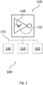
- Fig. 1 shows an FPGA device 100.
- the FPGA device 100 may be an AI accelerator FPGA device.
- the FPGA device 100 may be configured for performing autonomous driving calculations.
- the FPGA device 100 may be suitable for performing autonomous driving calculations.
- the autonomous driving calculations may comprise performing machine learning, or AI assisted calculations relating to the operation of an autonomous vehicle.
- the vehicle may be an autonomous road vehicle.
- the vehicle may be partially or fully autonomous in its operation.
- the vehicle may be an EV with an electrochemical battery and electrical propulsion means e.g. an electric motor.
- the FPGA device 100 may be installed in the vehicle.
- the FPGA device 100 may additionally find utility in a data center installation.
- the FPGA device 100 comprises a CLB 110.
- the FPGA device 100 may comprise a plurality of CLBs 110 as shown in Fig. 2 .
- the CLB 110 may be a K-input CLB, wherein K represents an integer corresponding to the number of inputs of the CLB 110.
- the integer K may e.g. be 3, 4, or 8.
- the CLB 110 may be configured for learning function mapping.
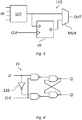
- the CLB 110 may be exemplified by Fig. 3 .
- the CLB 110 comprises at least one logic inverter 120.
- the LUT output is shown to connect to a input, referred to as input D, of a flip-flop, FF.
- the FF may be a so-called D-type FF.
- the LUT output line is also shown to connect to a multiplexer MUX.
- the FF may receive a further input in the form of a clock signal, CLK.
- the FF may provide an output, reffered to as output Q.
- the output Q is shown to connect to the MUX.
- the MUX may produce the CLB output signal, OUT.
- Fig. 4 shows a logic circuit diagram of a D-type FF.
- the FF may comprise a D input and a CLK input.
- the FF may comprise a Q output and a Q' output.
- the Q' output may be considered the inverse or complementing logical output to the Q output. E.g. if Q corresponds to a binary 1, Q' would correspond to a binary 0 and vice versa.
- the FF is shown to comprise a logic inverter 120 at the D input line. This logic inverter 120 may be considered the logic inverter of the CLB 110.
- the FF is further shown to comprise four logical NOT-AND, NAND, gates.
- the NAND gates may comprise a logical AND gate and a logical inverter 120.
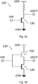
- the logic inverter 120 comprises at least one HEMT 130.
- Fig. 5a shows the logic inverter 120 comprising one HEMT 130.
- the HEMT130 is shown to be arranged as a pull-down network of the logic inverter 120.
- the logic inverter 120 comprises a resistor as its pull-up network, between the output line, VOUT, and the VDD node.
- the resistor may be realized as an always-on transistor with a specific on state resistance, thus corresponding to that of a discrete resistor.
- the logic inverter of Fig. 5a is a so-called 1 transistor, 1T, inverter.
- a high signal/binary 1 on the input line, VIN, connected to the HEMTs 130 gate node, may result in a low signal/binary 0 at VOUT and vice versa.
- the 1T inverter may see a direct current path between the VDD node and the ground node, GND, via the HEMTs 130 drain and source nodes, when the HEMTs 130 channel is open.
- Fig. 5b shows the logic inverter 120 comprising a pull-up transistor 230 instead of, as in Fig. 5a , having a resistor act as a pull-up network.
- the pull-up transistor 230 may be connected with its gate/base node to the input line, VIN.
- the pull-up transistor 230 may be connected with its source/emitter and drain/collector nodes connected to either one of the VDD and VOUT nodes.
- Such a logic inverter 120 may feature reduced leakage current from the VDD node to the GND node as the direct current path there between is only open for a short time during switching. Rise and fall times on the VOUT node may also be shorter due to this.
- the voltage at the VOUT node may also be larger than without a pull-up transistor 230.
- the pull-up transistor 230 may be a p-type MOSFET transistor, PMOS.
- the pull-up transistor 230 may be a Si-based transistor.
- the pull-up transistor 230 may be a Ge-based transistor.
- the pull-up transistor 230 may be a GaN/nitride-based transistor.
- the pull-up transistor 230 may be carbon nanotube-based transistor.
- the pull-up transistor 230 may be a high-hole-mobility transistor, HHMT.
- the pull-up transistor 230 may be a tunnel field-effect transistor, TFET.
- the pull-up transistor 230 may be a bipolar junction transistor, BJT.
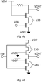
- Fig. 6a shows he logic inverter 120 being a cascode inverter.
- the logic inverter 120 may comprise at least two HEMTs 130.
- the two HEMTs 130 are shown to be arranged as a pull-down network of the logic inverter 120.
- a resistor is shown to form the pull-up network in a similar way to Fig. 5a .
- the top HEMT 130 is shown to be connected at its gate node to the VDD node. As such, the top HEMT 130 may be considered as an always-on transistor.
- the top HEMT 130 may additionally be considered a common gate stage of the cascode configured logic inverter 120.
- the bottom HEMT 130 is shown to be connected at its gate node to the input line, VIN.
- the bottom HEMT 130 may be considered as a common source stage of the cascode configured logic inverter 120.
- Fig. 6b shows the cascode configured logic inverter 120 comprising two pull-up transistors 230 as part of its pull-up network instead of the single resistor of Fig. 6a .
- the top pull-up transistor 230 is shown to be connected with its gate node to the input line, VIN.
- the top pull-up transistor 230 may be considered a common source/emitter stage of the cascode configured logic inverter 120.
- the bottom pull-up transistor 230 is shown to be connected with its gate node to the GND node.
- the bottom pull-up transistor 230 may be considered an always-on transistor.
- the bottom pull-up transistor 230 may additionally be considered a common gate stage of the cascode configured logic inverter 120.
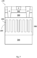
- the HEMT 130 comprises an Al y Ga y-1 N layer structure 380, wherein 0 ⁇ y ⁇ 1.
- the HEMT 130 also comprises a GaN layer structure 382.
- These layer structure features are not shown in Fig.1 but are instead shown in Fig. 7 , to which the readers attention is now directed.
- Fig. 7 shows a cross-sectional view of a HEMT 130 comprising the afforementioned layer structures 380, 382.
- Fig. 7 shows the HEMT 130 being based on a Si substrate 384.
- the Si substrate 384 may be a substantially monocrystalline Si structure.
- the Si substrate 384 may be a Si substrate with a ⁇ 111 > Miller index.
- the Si substrate 384 may be a Si wafer formed with the Czochralski process.
- the Si substrate 384 may be a chip or die from a larger Si wafer.
- Fig. 7 further shows a crystal transition structure 386 being formed on the Si substrate 384.
- the crystal transition structure 286 is shown to comprise a plurality of vertical nanowire structures 388.
- the vertical nanowire structures 388 are further shown to be perpendicularily arranged on the Si substrate 384.
- the vertical nanowire structures 388 may comprise GaN or AIN or AIGaN.
- Fig. 7 also shows the crystal transition structure 286 comprising an Al x Ga x-1 N layer structure 389, wherein 0 x ⁇ 1.
- the Al x Ga x-1 N layer structure 389 is shown to be arranged to vertically and laterally enclose the vertical nanowire strucutures 388.
- the Al x Ga x-1 N layer structure 389 may comprise a plurality of sublayers. The plurality of sublayers may feature a gradually decreasing value for the variable x.
- Fig. 7 shows the Al y Ga y-1 N layer structure 380 being arranged on the crystal transition structure 386 and the GaN layer structure 382 being arranged on the Al y Ga y-1 N layer structure 380.
- the GaN layer structure 382 may be arranged on the crystal transition structure 386 and the Al y Ga y-1 N layer structure 380 may be arranged on the GaN layer structure 382.
- Fig. 7 further shows source S, drain D, and gate G contacts of the HEMT 130.
- the drain contact D should not be confused with the input D of the flip-flop in either Fig. 3 or Fig. 4 .
- the contacts source, drain, and gate contacts may be formed by metal material.
- the source and drain contacts may comprise Ti, AI, Cu, Ni, and/or Au.
- the source and drain contacts may comprise compounds or alloys such as e.g. AICu.
- the gate contact may, in addition to the materials mentioned for the source and drain contacts, also or alternatively comprise Pd and/or Au. As for the source and drain contacts compounds and alloys are also options for the gate contact.
- each of the logic inverters 120 at least two HEMTs 130 comprise an Al y Ga y-1 N layer structure 380, and a GaN layer structure 382.
- the Al y Ga y-1 N layer structures 380 of each HEMT 130 of the logic inverter 120, cascode or otherwise configured, may be integrally formed.
- the GaN layer structures 382 of each HEMT 130 of the logic inverter 120, cascode or otherwise configured, may be integrally formed.
- the layer structures 380, 382 of HEMTs 130 may be separated by passivation/spacer structures to prevent the individual HEMTs 130 unintentionally affecting each other during operation.
- Fig. 1 shows that the FPGA device 100 may comprise a parallel shift register 140.
- the parallel shift register 140 may be a part of the CLB 110.
- the parallel shift register 140 may be considered to correspond to a LUT of the CLB 110 e.g. as the one shown in Fig. 3 .
- Fig. 1 further shows that the FPGA device 100 may comprise a memory block 150.
- the memory block 150 may be a part of the CLB 110.
- the memory block 150 may comprise a random-access memory, RAM.
- the RAM may be static, SRAM, or dynamic, DRAM.
- Other alternative memory solutions may include e.g. magnetoresistive RAM, MRAM.
- Fig. 1 and Fig. 3 further shows that the FPGA device 100 may comprise programmable I/O block(s) 160.
- Fig. 1 further shows that the FPGA device 100 may comprise an interconnect 170.
- the interconnect 170 may be configured to electrically connect at least two of the CLB 110, the parallel shift register 140, the memory block 150, and the programmable I/O block 160.
- Fig. 3 shows the interconnect 170 electrically connecting an array of CLBs 110 and programmable I/O blocks 160.
- the CLB 110, the parallel shift register 140, the memory block 150, and the programmable I/O block 160 may all be formed on a same Si substrate 384.
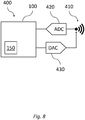
- Fig. 8 shows an Al processing system 400.
- the Al processing system 400 is shown to comprise the FPGA device 100.
- the FPGA device 100 may comprise a memory block 150.
- the memory block 150 may hold, or be configured to hold, stored instructions for operation the Al processing system 400.
- the Al processing system 400 is further shown to comprise a sensor 410.
- the sensor may provide, or be configured to provide, an analog sensor output signal.
- the sensor 410 may be e.g. a camera or stereo camera setup comprising image sensors, a radar/laser/acoustic range finder/object detection sensor, a microphone, an accelerometer, a gyroscope, a temperature sensor, a barometer, a motion sensor, a radio frequency sensor, etc.
- the Al processing system 400 is further shown to comprise an ADC 420.
- the ADC 420 may be provided or configured for receiving the sensor output signal, from the sensor 410, and processing the sensor output signal.
- the ADC 420 may process the analog sensor output signal as to provide a corresponding digital signal to the FPGA device 100.
- the ADC 420 may be a microchip type ADC.
- the an exemplary ADC 420 may be further described in the European Patent Application EP19205265 , which is hereby incorporated by reference.
- the block and circuit diagrams of Figures 1-2 and their corresponding passages in the text provide context to how the ADC 420 may be implemented.
- Figures 3-5 and their corresponding passages in the text provide context on the layer structures and HEMTs 130 of the present disclosure.
- the referenced application provides further context on integration of two HEMTs 130 in close proximity. This may provide improvements to e.g. the cascode configured logical inverters 120 of the FPGA device 100 as overall device footprint may be minimized.
- the summary of the referenced application provides further context on technical advantages and definitions of the language therein.
- the Al processing system 400 is further shown to comprise a DAC 430.
- the DAC 430 may be provided or configured for regulating the sensor 410.
- the DAC 430 may receive digital instructions from the FPGA device and provide a corresponding analog signal to the sensor 410.
- the DAC 430 may be a microchip type DAC.
Landscapes
- Physics & Mathematics (AREA)
- Mathematical Physics (AREA)
- Engineering & Computer Science (AREA)
- Computer Hardware Design (AREA)
- Computing Systems (AREA)
- General Engineering & Computer Science (AREA)
- Computer Networks & Wireless Communication (AREA)
- Junction Field-Effect Transistors (AREA)
- Logic Circuits (AREA)
- Analogue/Digital Conversion (AREA)
Priority Applications (8)
| Application Number | Priority Date | Filing Date | Title |
|---|---|---|---|
| EP20163052.2A EP3879706A1 (fr) | 2020-03-13 | 2020-03-13 | Dispositif de réseau prédiffusé programmable par l'utilisateur |
| CN202180018902.6A CN115336180A (zh) | 2020-03-13 | 2021-03-10 | 现场可编程门阵列器件 |
| EP21709722.9A EP4118748B1 (fr) | 2020-03-13 | 2021-03-10 | Dispositif de réseau prédiffusé programmable par l'utilisateur |
| EP24164179.4A EP4362096A3 (fr) | 2020-03-13 | 2021-03-10 | Dispositif de réseau prédiffusé programmable par l'utilisateur |
| TW110108578A TWI888500B (zh) | 2020-03-13 | 2021-03-10 | 現場可程式閘陣列元件與人工智慧處理系統 |
| US17/905,908 US11955972B2 (en) | 2020-03-13 | 2021-03-10 | Field-programmable gate array device |
| PCT/EP2021/055980 WO2021180757A1 (fr) | 2020-03-13 | 2021-03-10 | Dispositif prédiffusé programmable par utilisateur |
| US18/629,267 US12355442B2 (en) | 2020-03-13 | 2024-04-08 | Field-programmable gate array device |
Applications Claiming Priority (1)
| Application Number | Priority Date | Filing Date | Title |
|---|---|---|---|
| EP20163052.2A EP3879706A1 (fr) | 2020-03-13 | 2020-03-13 | Dispositif de réseau prédiffusé programmable par l'utilisateur |
Publications (1)
| Publication Number | Publication Date |
|---|---|
| EP3879706A1 true EP3879706A1 (fr) | 2021-09-15 |
Family
ID=69941146
Family Applications (3)
| Application Number | Title | Priority Date | Filing Date |
|---|---|---|---|
| EP20163052.2A Withdrawn EP3879706A1 (fr) | 2020-03-13 | 2020-03-13 | Dispositif de réseau prédiffusé programmable par l'utilisateur |
| EP24164179.4A Pending EP4362096A3 (fr) | 2020-03-13 | 2021-03-10 | Dispositif de réseau prédiffusé programmable par l'utilisateur |
| EP21709722.9A Active EP4118748B1 (fr) | 2020-03-13 | 2021-03-10 | Dispositif de réseau prédiffusé programmable par l'utilisateur |
Family Applications After (2)
| Application Number | Title | Priority Date | Filing Date |
|---|---|---|---|
| EP24164179.4A Pending EP4362096A3 (fr) | 2020-03-13 | 2021-03-10 | Dispositif de réseau prédiffusé programmable par l'utilisateur |
| EP21709722.9A Active EP4118748B1 (fr) | 2020-03-13 | 2021-03-10 | Dispositif de réseau prédiffusé programmable par l'utilisateur |
Country Status (5)
| Country | Link |
|---|---|
| US (2) | US11955972B2 (fr) |
| EP (3) | EP3879706A1 (fr) |
| CN (1) | CN115336180A (fr) |
| TW (1) | TWI888500B (fr) |
| WO (1) | WO2021180757A1 (fr) |
Families Citing this family (7)
| Publication number | Priority date | Publication date | Assignee | Title |
|---|---|---|---|---|
| EP3785289B1 (fr) | 2018-04-22 | 2025-12-24 | Epinovatech AB | Dispositif à film mince renforcé |
| EP3855530B1 (fr) | 2020-01-24 | 2025-04-16 | Epinovatech AB | Batterie à semi-conducteurs |
| EP3866189B1 (fr) | 2020-02-14 | 2022-09-28 | Epinovatech AB | Module mmic frontal |
| EP3879706A1 (fr) | 2020-03-13 | 2021-09-15 | Epinovatech AB | Dispositif de réseau prédiffusé programmable par l'utilisateur |
| EP3907877A1 (fr) | 2020-05-07 | 2021-11-10 | Epinovatech AB | Machine à induction |
| EP3916804A1 (fr) | 2020-05-29 | 2021-12-01 | Epinovatech AB | Hemt vertical et procédé de fabrication d'un hemt vertical |
| EP4090139B1 (fr) | 2021-05-10 | 2023-10-25 | Epinovatech AB | Dispositif convertisseur de puissance |
Citations (3)
| Publication number | Priority date | Publication date | Assignee | Title |
|---|---|---|---|---|
| US20070295993A1 (en) * | 2005-11-29 | 2007-12-27 | The Hong Kong University Of Science And Technology | Low Density Drain HEMTs |
| CN101621292B (zh) * | 2009-04-10 | 2012-05-09 | 浙江大学 | 开关电容积分器 |
| US20140134773A1 (en) * | 2011-10-10 | 2014-05-15 | Sensor Electronic Technology, Inc. | Patterned Layer Design for Group III Nitride Layer Growth |
Family Cites Families (155)
| Publication number | Priority date | Publication date | Assignee | Title |
|---|---|---|---|---|
| US2463073A (en) | 1945-01-26 | 1949-03-01 | Rca Corp | Oscillator |
| US4103325A (en) | 1977-03-18 | 1978-07-25 | Sperry Rand Corporation | Aircraft power and phase converter |
| EP0284700A1 (fr) | 1987-03-31 | 1988-10-05 | Marthaler, Willy | Objet de maintien d'une pièce d'horlogerie et/ou de bijouterie destiné â être porté par une personne |
| US4873497A (en) | 1988-10-03 | 1989-10-10 | Motorola, Inc. | Wide band voltage controlled R-C oscillator for use with MMIC technology |
| WO1995008452A1 (fr) | 1993-09-23 | 1995-03-30 | Stichting Voor De Technische Wetenschappen | Procede et circuit de commande d'un moteur a induction |
| EP1016129B2 (fr) | 1997-06-24 | 2009-06-10 | Massachusetts Institute Of Technology | Regulation des densites de dislocation filetees au moyen de couches a teneur echelonnee et d'une planarisation |
| JP2000101152A (ja) | 1998-09-24 | 2000-04-07 | Citizen Watch Co Ltd | 熱電素子 |
| US20030022395A1 (en) | 2001-07-17 | 2003-01-30 | Thoughtbeam, Inc. | Structure and method for fabricating an integrated phased array circuit |
| JP2003101069A (ja) | 2001-09-25 | 2003-04-04 | Nagoya Industrial Science Research Inst | Iii族窒化物量子ドットおよびその製造方法 |
| US7189430B2 (en) | 2002-02-11 | 2007-03-13 | Rensselaer Polytechnic Institute | Directed assembly of highly-organized carbon nanotube architectures |
| JP2004222486A (ja) | 2002-12-27 | 2004-08-05 | Murata Mfg Co Ltd | スイッチング電源モジュール |
| KR100593264B1 (ko) | 2003-06-26 | 2006-06-26 | 학교법인 포항공과대학교 | p-타입 반도체 박막과 n-타입 산화아연(ZnO)계나노막대의 이종접합 구조체, 이의 제법 및 이를 이용한소자 |
| US20050064291A1 (en) | 2003-09-18 | 2005-03-24 | Matsushita Electric Industrial Co., Ltd. | Battery and non-aqueous electrolyte secondary battery using the same |
| US7148149B2 (en) | 2003-12-24 | 2006-12-12 | Matsushita Electric Industrial Co., Ltd. | Method for fabricating nitride-based compound semiconductor element |
| JP4523306B2 (ja) | 2004-03-19 | 2010-08-11 | シチズンホールディングス株式会社 | 熱電素子の製造方法 |
| US7745376B2 (en) | 2004-08-10 | 2010-06-29 | Nove Technologies, Inc. | Superconducting composite |
| KR100664986B1 (ko) | 2004-10-29 | 2007-01-09 | 삼성전기주식회사 | 나노로드를 이용한 질화물계 반도체 소자 및 그 제조 방법 |
| US7202173B2 (en) | 2004-12-20 | 2007-04-10 | Palo Alto Research Corporation Incorporated | Systems and methods for electrical contacts to arrays of vertically aligned nanorods |
| US20070108435A1 (en) | 2005-02-07 | 2007-05-17 | Harmon Eric S | Method of making nanowires |
| TWI252920B (en) | 2005-03-25 | 2006-04-11 | Ind Tech Res Inst | Method of fabricating an integral device of a biochip integrated with micro thermo-electric elements and the apparatus thereof |
| US8324660B2 (en) | 2005-05-17 | 2012-12-04 | Taiwan Semiconductor Manufacturing Company, Ltd. | Lattice-mismatched semiconductor structures with reduced dislocation defect densities and related methods for device fabrication |
| JP5113330B2 (ja) | 2005-11-30 | 2013-01-09 | ローム株式会社 | 窒化ガリウム半導体発光素子 |
| AU2007313096B2 (en) | 2006-03-10 | 2011-11-10 | Unm Rainforest Innovations | Pulsed growth of GaN nanowires and applications in group III nitride semiconductor substrate materials and devices |
| US7968359B2 (en) | 2006-03-10 | 2011-06-28 | Stc.Unm | Thin-walled structures |
| DE112007000667T5 (de) | 2006-03-20 | 2009-01-29 | International Rectifier Corp., El Segundo | Vereinigter Gate-Kaskoden-Transistor |
| US20070277866A1 (en) | 2006-05-31 | 2007-12-06 | General Electric Company | Thermoelectric nanotube arrays |
| JP4807186B2 (ja) | 2006-08-30 | 2011-11-02 | マツダ株式会社 | フリーピストンエンジンの制御装置 |
| KR20090075819A (ko) | 2006-09-19 | 2009-07-09 | 큐나노 에이비 | 나노스케일 전계 효과 트랜지스터의 조립체 |
| US7902809B2 (en) | 2006-11-28 | 2011-03-08 | International Rectifier Corporation | DC/DC converter including a depletion mode power switch |
| FR2910721B1 (fr) | 2006-12-21 | 2009-03-27 | Commissariat Energie Atomique | Ensemble collecteur de courant-electrode avec des cavites d'expansion pour accumulateur au lithium sous forme de films minces. |
| EP2102899B1 (fr) | 2007-01-12 | 2020-11-11 | QuNano AB | Nanofils de nitrure et leur procede de fabrication |
| US20080171424A1 (en) | 2007-01-16 | 2008-07-17 | Sharp Laboratories Of America, Inc. | Epitaxial growth of GaN and SiC on silicon using nanowires and nanosize nucleus methodologies |
| GB0702560D0 (en) | 2007-02-09 | 2007-03-21 | Univ Bath | Production of Semiconductor devices |
| US8094223B1 (en) * | 2007-05-30 | 2012-01-10 | On Semiconductor Trading Ltd. | Bus driving in an image sensor |
| JP5341325B2 (ja) | 2007-07-25 | 2013-11-13 | 日本化学工業株式会社 | リチウム二次電池用正極活物質、その製造方法及びリチウム二次電池 |
| WO2009035746A2 (fr) | 2007-09-07 | 2009-03-19 | Amberwave Systems Corporation | Cellules solaires multi-jonctions |
| EP2075745A1 (fr) | 2007-12-28 | 2009-07-01 | Hitachi Ltd. | Dispositif de traitement d'informations quantiques |
| WO2009135078A2 (fr) | 2008-04-30 | 2009-11-05 | The Regents Of The University Of California | Procédé et appareil de fabrication de dispositifs opto-électromécaniques par transfert de structure avec utilisation d’un substrat réutilisable |
| US8957642B2 (en) | 2008-05-06 | 2015-02-17 | International Rectifier Corporation | Enhancement mode III-nitride switch with increased efficiency and operating frequency |
| KR101563554B1 (ko) | 2008-08-01 | 2015-10-27 | 퀄컴 테크놀로지스, 인크. | 잡음 제거를 위한 통합 시간 필터를 구비한 비디오 인코더 |
| US20110140072A1 (en) | 2008-08-21 | 2011-06-16 | Nanocrystal Corporation | Defect-free group iii - nitride nanostructures and devices using pulsed and non-pulsed growth techniques |
| US20100072515A1 (en) | 2008-09-19 | 2010-03-25 | Amberwave Systems Corporation | Fabrication and structures of crystalline material |
| US8305025B2 (en) | 2008-10-07 | 2012-11-06 | Siemens Industry, Inc. | Methods and apparatus for controlling multiple A.C. induction machines from a single inverter |
| US9275857B1 (en) | 2008-12-19 | 2016-03-01 | Stc.Unm | Nanowires, nanowire networks and methods for their formation and use |
| WO2010100599A1 (fr) | 2009-03-04 | 2010-09-10 | Koninklijke Philips Electronics, N.V. | Batterie à film mince de grande capacité et son procédé de fabrication |
| TW201036347A (en) | 2009-03-23 | 2010-10-01 | Ralink Technology Corp | Radio frequency transceiver and related wireless communication device |
| JP5182189B2 (ja) | 2009-03-27 | 2013-04-10 | 富士通株式会社 | 半導体装置の製造方法 |
| US9502973B2 (en) | 2009-04-08 | 2016-11-22 | Infineon Technologies Americas Corp. | Buck converter with III-nitride switch for substantially increased input-to-output voltage ratio |
| JP5299105B2 (ja) | 2009-06-16 | 2013-09-25 | ソニー株式会社 | 二酸化バナジウムナノワイヤとその製造方法、及び二酸化バナジウムナノワイヤを用いたナノワイヤデバイス |
| JP4700125B2 (ja) | 2009-07-30 | 2011-06-15 | 住友電気工業株式会社 | 半導体装置およびその製造方法 |
| WO2011067872A1 (fr) | 2009-12-01 | 2011-06-09 | 国立大学法人北海道大学 | Élément électroluminescent et son procédé de fabrication |
| US8604498B2 (en) | 2010-03-26 | 2013-12-10 | Tsmc Solid State Lighting Ltd. | Single phosphor layer photonic device for generating white light or color lights |
| US8692105B2 (en) | 2010-04-16 | 2014-04-08 | The Regents Of The University Of California | III-V nitride-based thermoelectric device |
| US9114399B2 (en) | 2010-08-31 | 2015-08-25 | Canon U.S. Life Sciences, Inc. | System and method for serial processing of multiple nucleic acid assays |
| EP2571065A4 (fr) | 2010-12-08 | 2016-03-23 | El Seed Corp | Dispositif à semi-conducteur à nitrure du groupe iii et procédé de fabrication associé |
| GB201021112D0 (en) | 2010-12-13 | 2011-01-26 | Ntnu Technology Transfer As | Nanowires |
| WO2012105901A1 (fr) | 2011-02-01 | 2012-08-09 | Qunano Ab | Batterie au lithium-ion comportant des nanofils |
| JP5123414B2 (ja) | 2011-05-16 | 2013-01-23 | 株式会社東芝 | 半導体発光素子、窒化物半導体ウェーハ及び窒化物半導体層の製造方法 |
| US10312361B2 (en) | 2011-06-20 | 2019-06-04 | The Regents Of The University Of California | Trenched vertical power field-effect transistors with improved on-resistance and breakdown voltage |
| US8758480B2 (en) | 2011-09-09 | 2014-06-24 | Torosoleil, Llc | Dynamic and continuous control for pressure swing adsorption |
| JP5857573B2 (ja) | 2011-09-16 | 2016-02-10 | 富士通株式会社 | 化合物半導体装置の製造方法 |
| WO2013049817A1 (fr) | 2011-09-30 | 2013-04-04 | The Regents Of The University Of California | Dispositifs opto-électriques à affaissement du rendement et tension directe réduits |
| US8884308B2 (en) * | 2011-11-29 | 2014-11-11 | Taiwan Semiconductor Manufacturing Company, Ltd. | High electron mobility transistor structure with improved breakdown voltage performance |
| GB201200355D0 (en) | 2012-01-10 | 2012-02-22 | Norwegian Univ Sci & Tech Ntnu | Nanowires |
| JP2013153027A (ja) | 2012-01-24 | 2013-08-08 | Fujitsu Ltd | 半導体装置及び電源装置 |
| WO2013121289A2 (fr) | 2012-02-14 | 2013-08-22 | Qunano Ab | Electronique à base de nanofil de nitrure de gallium |
| CN103531474B (zh) | 2012-07-02 | 2016-04-20 | 中国科学院微电子研究所 | 半导体器件制造方法 |
| TWI617045B (zh) | 2012-07-06 | 2018-03-01 | Epistar Corporation | 具有奈米柱之發光元件及其製造方法 |
| JP6048026B2 (ja) | 2012-09-20 | 2016-12-21 | 富士通株式会社 | 電源回路及び電源装置 |
| FR3000294B1 (fr) | 2012-12-21 | 2016-03-04 | Aledia | Support fonctionnel comprenant des nanofils et des nano-empreintes et procede de fabrication dudit support |
| JP2014127708A (ja) | 2012-12-27 | 2014-07-07 | Toshiba Corp | 半導体発光素子及び半導体発光素子の製造方法 |
| US9251934B2 (en) | 2013-01-11 | 2016-02-02 | Infineon Technologies Ag | Method for manufacturing a plurality of nanowires |
| JP6161910B2 (ja) | 2013-01-30 | 2017-07-12 | ルネサスエレクトロニクス株式会社 | 半導体装置 |
| US20160005919A1 (en) | 2013-02-05 | 2016-01-07 | Tokuyama Corporation | Nitride semiconductor light emitting device |
| US8823146B1 (en) | 2013-02-19 | 2014-09-02 | Raytheon Company | Semiconductor structure having silicon devices, column III-nitride devices, and column III-non-nitride or column II-VI devices |
| US8946779B2 (en) | 2013-02-26 | 2015-02-03 | Freescale Semiconductor, Inc. | MISHFET and Schottky device integration |
| CN103236477B (zh) | 2013-04-19 | 2015-08-12 | 安徽三安光电有限公司 | 一种led外延结构及其制备方法 |
| JP2014217252A (ja) | 2013-04-30 | 2014-11-17 | 三菱電機株式会社 | カスコード接続パワーデバイス |
| US9349715B2 (en) | 2013-06-21 | 2016-05-24 | Infineon Technologies Americas Corp. | Depletion mode group III-V transistor with high voltage group IV enable switch |
| JP6175931B2 (ja) | 2013-06-21 | 2017-08-09 | 富士通株式会社 | 導電構造及びその製造方法、電子装置及びその製造方法 |
| US9419194B2 (en) | 2013-08-13 | 2016-08-16 | Palo Alto Research Center Incorporated | Transparent electron blocking hole transporting layer |
| US9764950B2 (en) | 2013-08-16 | 2017-09-19 | Taiwan Semiconductor Manufacturing Company Limited | Semiconductor arrangement with one or more semiconductor columns |
| US9640645B2 (en) | 2013-09-05 | 2017-05-02 | Taiwan Semiconductor Manufacturing Company Limited | Semiconductor device with silicide |
| JP6237038B2 (ja) | 2013-09-20 | 2017-11-29 | 富士通株式会社 | カスコードトランジスタ及びカスコードトランジスタの制御方法 |
| US20150118572A1 (en) | 2013-10-29 | 2015-04-30 | Battery Energy Storage Systems-Technologies | Solid-state battery and methods of fabrication |
| GB2520687A (en) | 2013-11-27 | 2015-06-03 | Seren Photonics Ltd | Semiconductor devices and fabrication methods |
| US9379657B2 (en) | 2013-12-16 | 2016-06-28 | Wisconsin Alumni Research Foundation | Unity power factor induction machine |
| US9472625B2 (en) | 2014-03-17 | 2016-10-18 | Infineon Technologies Austria Ag | Operational Gallium Nitride devices |
| WO2015159348A1 (fr) | 2014-04-14 | 2015-10-22 | 富士通株式会社 | Appareil photosynthétique |
| GB201407297D0 (en) | 2014-04-25 | 2014-06-11 | Gasp Solar Aps | A method of preparing a substrate for nanowire growth, And a method of fabricating an array of semiconductor nanostructures |
| US9893174B2 (en) | 2014-05-21 | 2018-02-13 | Arizona Board Of Regents On Behalf Of Arizona State University | III-nitride based N polar vertical tunnel transistor |
| US9773669B2 (en) | 2014-09-11 | 2017-09-26 | Ramot At Tel-Aviv University Ltd. | Method of fabricating a nanoribbon and applications thereof |
| US9406506B2 (en) | 2014-11-05 | 2016-08-02 | International Business Machines Corporation | Lattice matched aspect ratio trapping to reduce defects in III-V layer directly grown on silicon |
| DE102015200742A1 (de) | 2015-01-20 | 2016-07-21 | Zf Friedrichshafen Ag | Steuerung einer Drehfeldmaschine |
| US9520466B2 (en) | 2015-03-16 | 2016-12-13 | Taiwan Semiconductor Manufacturing Company, Ltd. | Vertical gate-all-around field effect transistors and methods of forming same |
| US11978731B2 (en) | 2015-09-21 | 2024-05-07 | Monolithic 3D Inc. | Method to produce a multi-level semiconductor memory device and structure |
| US9887637B1 (en) * | 2015-06-16 | 2018-02-06 | Tagore Technology, Inc. | High speed programmable threshold gallium nitride power limiter |
| CN106549050A (zh) | 2015-09-17 | 2017-03-29 | 中国科学院苏州纳米技术与纳米仿生研究所 | 级联增强型hemt器件 |
| US9916985B2 (en) | 2015-10-14 | 2018-03-13 | International Business Machines Corporation | Indium phosphide smoothing and chemical mechanical planarization processes |
| US10439671B2 (en) | 2015-12-21 | 2019-10-08 | Intel Corporation | Microelectronic devices designed with high frequency communication modules having steerable beamforming capability |
| US9947591B2 (en) | 2015-12-22 | 2018-04-17 | Imec Vzw | Method for manufacturing a Si-based high-mobility CMOS device with stacked channel layers, and resulting devices |
| WO2017111844A1 (fr) | 2015-12-24 | 2017-06-29 | Intel Corporation | Dispositifs mémoires comprenant une diode tunnel intégrée en contact et leurs techniques de fabrication |
| US11018253B2 (en) | 2016-01-07 | 2021-05-25 | Lawrence Livermore National Security, Llc | Three dimensional vertically structured electronic devices |
| US10128750B2 (en) | 2016-03-04 | 2018-11-13 | Infineon Technologies Ag | Switched-mode power converter with an inductive storage element and a cascode circuit |
| US11239394B2 (en) | 2016-03-18 | 2022-02-01 | Lg Innotek Co., Ltd. | Semiconductor device and display device including the same |
| CN105895526B (zh) | 2016-04-26 | 2019-02-01 | 中国科学院微电子研究所 | 一种GaN基功率电子器件及其制备方法 |
| US10192976B2 (en) | 2016-04-28 | 2019-01-29 | The Trustees Of Princeton University | Semiconductor quantum dot device and method for forming a scalable linear array of quantum dots |
| CN105914232B (zh) | 2016-05-06 | 2020-02-21 | 西安电子科技大学 | T栅N面GaN/AlGaN鳍式高电子迁移率晶体管 |
| US10312082B2 (en) | 2016-05-09 | 2019-06-04 | The Regents Of The University Of Michigan | Metal based nanowire tunnel junctions |
| US9941330B2 (en) | 2016-05-18 | 2018-04-10 | Globalfoundries Inc. | LEDs with three color RGB pixels for displays |
| WO2017213644A1 (fr) | 2016-06-08 | 2017-12-14 | Intel Corporation | Intégration monolithique d'un transistor à canal p d'arrière-plan avec un transistor à canal n de type iii-n |
| US10211329B2 (en) * | 2016-06-16 | 2019-02-19 | Infineon Technologies Americas Corp. | Charge trapping prevention III-Nitride transistor |
| US10516050B2 (en) | 2016-07-29 | 2019-12-24 | Taiwan Semiconductor Manufacturing Co., Ltd. | Method for forming stressor, semiconductor device having stressor, and method for forming the same |
| WO2018084878A1 (fr) | 2016-11-03 | 2018-05-11 | Intel Corporation | Dispositifs à points quantiques |
| BR102016026339B1 (pt) | 2016-11-10 | 2022-08-02 | Embraco Indústria De Compressores E Soluções E Refrigeração Ltda | Sistema e método de partida para um motor de indução monofásico |
| US10840092B2 (en) | 2016-11-29 | 2020-11-17 | Unm Rainforest Innovations | Atomic force microscopy based on nanowire tips for high aspect ratio nanoscale metrology/confocal microscopy |
| US10479218B2 (en) | 2017-02-14 | 2019-11-19 | Toyota Motor Engineering & Manufacturing North America, Inc. | Electric vehicle power system with shared converter |
| WO2019003047A1 (fr) * | 2017-06-27 | 2019-01-03 | 株式会社半導体エネルギー研究所 | Dispositif à semi-conducteur et procédé de fabrication de dispositif à semi-conducteur |
| US10387792B1 (en) | 2017-06-29 | 2019-08-20 | Hrl Laboratories, Llc | Etched spin-qubit for high temperature operation |
| US10446681B2 (en) | 2017-07-10 | 2019-10-15 | Micron Technology, Inc. | NAND memory arrays, and devices comprising semiconductor channel material and nitrogen |
| US10553712B2 (en) | 2017-07-12 | 2020-02-04 | Indian Institute Of Technology | High-electron-mobility transistor (HEMT) |
| TW201914026A (zh) * | 2017-09-08 | 2019-04-01 | 聯穎光電股份有限公司 | 氮化物半導體元件 |
| US10475929B2 (en) | 2017-11-30 | 2019-11-12 | Taiwan Semiconductor Manufacturing Co., Ltd. | Semiconductor device and manufacturing method thereof |
| WO2019147738A1 (fr) | 2018-01-23 | 2019-08-01 | Light Share, LLC | Pixels micro-del monolithiques à pleine couleur |
| GB201801337D0 (en) | 2018-01-26 | 2018-03-14 | Cambridge Entpr Ltd | Method for etching a semiconductor structure |
| WO2019144966A1 (fr) | 2018-01-29 | 2019-08-01 | Coyote Bioscience Co., Ltd. | Systèmes et procédés d'analyse d'acides nucléiques |
| JP6816735B2 (ja) | 2018-03-13 | 2021-01-20 | 株式会社豊田中央研究所 | 化学反応用電極、それを用いた化学反応用セル及び化学反応装置 |
| CN110324568B (zh) * | 2018-03-29 | 2021-07-09 | 赛灵思电子科技(北京)有限公司 | 一种网络视频监控装置 |
| US10742208B1 (en) * | 2018-04-13 | 2020-08-11 | Hrl Laboratories, Llc | Circuit for driving switched transistor and filter, circulator and correlator including the same |
| FR3080487B1 (fr) | 2018-04-20 | 2020-06-12 | Commissariat A L'energie Atomique Et Aux Energies Alternatives | Procede de fabrication d’un dispositif optoelectronique a matrice de diodes |
| EP3785289B1 (fr) | 2018-04-22 | 2025-12-24 | Epinovatech AB | Dispositif à film mince renforcé |
| TWI701835B (zh) * | 2018-05-04 | 2020-08-11 | 晶元光電股份有限公司 | 高電子遷移率電晶體 |
| US10594268B2 (en) | 2018-05-18 | 2020-03-17 | Cree, Inc. | Switch circuits having integrated overdrive protection and related transmit/receive circuits and MMIC amplifiers |
| US10535570B1 (en) | 2018-06-22 | 2020-01-14 | International Business Machines Corporation | Cointegration of III-V channels and germanium channels for vertical field effect transistors |
| US10811588B2 (en) | 2018-08-06 | 2020-10-20 | International Business Machines Corporation | Vertical dispersive readout of qubits of a lattice surface code architecture |
| FR3091022B1 (fr) | 2018-12-20 | 2020-12-11 | Commissariat Energie Atomique | Procede de fabrication de structures optoelectroniques pourvues de diodes electroluminescentes coplanaires |
| US11243098B2 (en) * | 2019-02-08 | 2022-02-08 | Simmonds Precision Products, Inc. | Configurable nodes for sensing systems |
| CN110336028B (zh) | 2019-04-30 | 2021-03-30 | 中国科学院半导体研究所 | 电池负极材料及其制备方法、锂电池 |
| WO2020222149A1 (fr) | 2019-05-02 | 2020-11-05 | Epitronic Holdings Pte. Ltd. | Capteur microélectronique à détecteur bolométrique ou pyroélectrique permettant la détection de signaux électriques dans des gammes de fréquences infra-térahertz et térahertz |
| US11411099B2 (en) | 2019-05-28 | 2022-08-09 | Glc Semiconductor Group (Cq) Co., Ltd. | Semiconductor device |
| WO2021021415A1 (fr) | 2019-07-28 | 2021-02-04 | Applied Materials, Inc. | Micro-del et procédé de fabrication de micro-del |
| CN112490243B (zh) * | 2019-09-12 | 2023-09-12 | 联华电子股份有限公司 | 三维半导体结构及其制作方法 |
| EP3813240A1 (fr) | 2019-10-25 | 2021-04-28 | Epinovatech AB | Circuit convertisseur ca-cc |
| EP3836227A1 (fr) | 2019-12-11 | 2021-06-16 | Epinovatech AB | Structure à couches semi-conductrices |
| EP3855530B1 (fr) | 2020-01-24 | 2025-04-16 | Epinovatech AB | Batterie à semi-conducteurs |
| EP3866189B1 (fr) | 2020-02-14 | 2022-09-28 | Epinovatech AB | Module mmic frontal |
| US11621598B2 (en) | 2020-03-10 | 2023-04-04 | Qatar University | Torque density pseudo six-phase induction machine |
| EP3879706A1 (fr) | 2020-03-13 | 2021-09-15 | Epinovatech AB | Dispositif de réseau prédiffusé programmable par l'utilisateur |
| EP3907877A1 (fr) | 2020-05-07 | 2021-11-10 | Epinovatech AB | Machine à induction |
| EP3916804A1 (fr) | 2020-05-29 | 2021-12-01 | Epinovatech AB | Hemt vertical et procédé de fabrication d'un hemt vertical |
| EP4080575A1 (fr) | 2021-04-22 | 2022-10-26 | Epinovatech AB | Procédé pour former une matrice d'éléments dels de différentes couleurs |
| EP4090139B1 (fr) | 2021-05-10 | 2023-10-25 | Epinovatech AB | Dispositif convertisseur de puissance |
| EP4101945B1 (fr) | 2021-06-09 | 2024-05-15 | Epinovatech AB | Dispositif pour effectuer une électrolyse de l'eau et système associé |
| EP4125135A1 (fr) | 2021-07-28 | 2023-02-01 | Epinovatech AB | Transistor, dispositif électrique et procédé de production d'un transistor |
| EP4187616A1 (fr) | 2021-11-26 | 2023-05-31 | Epinovatech AB | Hemt vertical, circuit électrique, et procédé de production d'un hemt vertical |
-
2020
- 2020-03-13 EP EP20163052.2A patent/EP3879706A1/fr not_active Withdrawn
-
2021
- 2021-03-10 EP EP24164179.4A patent/EP4362096A3/fr active Pending
- 2021-03-10 EP EP21709722.9A patent/EP4118748B1/fr active Active
- 2021-03-10 WO PCT/EP2021/055980 patent/WO2021180757A1/fr not_active Ceased
- 2021-03-10 CN CN202180018902.6A patent/CN115336180A/zh active Pending
- 2021-03-10 TW TW110108578A patent/TWI888500B/zh active
- 2021-03-10 US US17/905,908 patent/US11955972B2/en active Active
-
2024
- 2024-04-08 US US18/629,267 patent/US12355442B2/en active Active
Patent Citations (3)
| Publication number | Priority date | Publication date | Assignee | Title |
|---|---|---|---|---|
| US20070295993A1 (en) * | 2005-11-29 | 2007-12-27 | The Hong Kong University Of Science And Technology | Low Density Drain HEMTs |
| CN101621292B (zh) * | 2009-04-10 | 2012-05-09 | 浙江大学 | 开关电容积分器 |
| US20140134773A1 (en) * | 2011-10-10 | 2014-05-15 | Sensor Electronic Technology, Inc. | Patterned Layer Design for Group III Nitride Layer Growth |
Non-Patent Citations (3)
| Title |
|---|
| PAUL SRITOMA ET AL: "A Novel GaN-Hemt based Inverter and Cascode Amplifier", 2018 IEEE ELECTRON DEVICES KOLKATA CONFERENCE (EDKCON), IEEE, 24 November 2018 (2018-11-24), pages 465 - 469, XP033580758, DOI: 10.1109/EDKCON.2018.8770510 * |
| TAVARES GABRIEL H M ET AL: "Implementation of a high frequency PWM signal in FPGA FOR GaN power devices switching", 2017 BRAZILIAN POWER ELECTRONICS CONFERENCE (COBEP), IEEE, 19 November 2017 (2017-11-19), pages 1 - 7, XP033297053, DOI: 10.1109/COBEP.2017.8257309 * |
| Y. CAI ET AL: "Monolithically Integrated Enhancement/Depletion-Mode AlGaN/GaN HEMT Inverters and Ring Oscillators Using$hboxCF_4$Plasma Treatment", IEEE TRANSACTIONS ON ELECTRON DEVICES, vol. 53, no. 9, 1 September 2006 (2006-09-01), US, pages 2223 - 2230, XP055732103, ISSN: 0018-9383, DOI: 10.1109/TED.2005.881002 * |
Also Published As
| Publication number | Publication date |
|---|---|
| WO2021180757A1 (fr) | 2021-09-16 |
| EP4118748B1 (fr) | 2024-04-24 |
| EP4362096A2 (fr) | 2024-05-01 |
| TW202207632A (zh) | 2022-02-16 |
| US11955972B2 (en) | 2024-04-09 |
| US12355442B2 (en) | 2025-07-08 |
| EP4118748C0 (fr) | 2024-04-24 |
| EP4362096A3 (fr) | 2024-07-31 |
| US20230119801A1 (en) | 2023-04-20 |
| EP4118748A1 (fr) | 2023-01-18 |
| CN115336180A (zh) | 2022-11-11 |
| TWI888500B (zh) | 2025-07-01 |
| US20240250686A1 (en) | 2024-07-25 |
Similar Documents
| Publication | Publication Date | Title |
|---|---|---|
| EP4118748B1 (fr) | Dispositif de réseau prédiffusé programmable par l'utilisateur | |
| US6326666B1 (en) | DTCMOS circuit having improved speed | |
| Trescases et al. | GaN power ICs: Reviewing strengths, gaps, and future directions | |
| JP5356536B2 (ja) | 電圧レベル変換回路 | |
| Abe et al. | New technology towards GaAs LSI/VLSI for computer applications | |
| US7994550B2 (en) | Semiconductor structures having both elemental and compound semiconductor devices on a common substrate | |
| US20140070627A1 (en) | Integrated Group III-V Power Stage | |
| CN104377201A (zh) | 互补氮化镓集成电路及其制作方法 | |
| CN115485827A (zh) | 具有共享电极的集成晶体管 | |
| CN107170673A (zh) | 具有石墨烯掩埋散热层和源接地的GaNMMIC器件及制备方法 | |
| US20240322814A1 (en) | Buffer circuit for driving a gan power switch and corresponding driver circuit | |
| CN111897209B (zh) | 一种毫米波芯片增益高低温自适应偏置结构及方法 | |
| Raghavan et al. | Indium phosphide ICs unleash the high-frequency spectrum | |
| HK40108694A (en) | Field-programmable gate array device | |
| CN217508742U (zh) | 复合逻辑门电路及包括其的芯片和电子装置 | |
| JPH08204536A (ja) | インタフェース回路及びレベル変換回路 | |
| TWI523148B (zh) | 提升高電子遷移率電晶體元件崩潰電壓的方法 | |
| US9438112B2 (en) | Power converter including integrated driver for depletion mode group III-V transistor | |
| Cui et al. | A monolithic GaN driver with a deadtime generator (DTG) for high‐temperature (HT) GaN DC‐DC buck converters | |
| Stesev et al. | Serial-to-parallel converter using GaAs D-mode transistors | |
| CN105680107B (zh) | 一种基于soi工艺的电池管理芯片电路 | |
| US10923473B2 (en) | High voltage logic circuit | |
| Mizutani et al. | Gigabit logic operation with enhancement-mode GaAs MESFET IC's | |
| Fan et al. | Wafer-Scale GaN-Si (100) Monolithic Heterogeneous Integration Inverters With Improved Output Voltage Swing and Fast Switching Capability by Transfer Printing and Self-Aligned Etching Technology | |
| Choi et al. | Monolithically integrated GaN+ CMOS logic circuits design and electro-thermal analysis for high-voltage applications |
Legal Events
| Date | Code | Title | Description |
|---|---|---|---|
| PUAI | Public reference made under article 153(3) epc to a published international application that has entered the european phase |
Free format text: ORIGINAL CODE: 0009012 |
|
| STAA | Information on the status of an ep patent application or granted ep patent |
Free format text: STATUS: THE APPLICATION HAS BEEN PUBLISHED |
|
| AK | Designated contracting states |
Kind code of ref document: A1 Designated state(s): AL AT BE BG CH CY CZ DE DK EE ES FI FR GB GR HR HU IE IS IT LI LT LU LV MC MK MT NL NO PL PT RO RS SE SI SK SM TR |
|
| STAA | Information on the status of an ep patent application or granted ep patent |
Free format text: STATUS: THE APPLICATION IS DEEMED TO BE WITHDRAWN |
|
| 18D | Application deemed to be withdrawn |
Effective date: 20220316 |