EP4517439A2 - Systèmes et procédés de fabrication de cellules de guide d'ondes - Google Patents
Systèmes et procédés de fabrication de cellules de guide d'ondes Download PDFInfo
- Publication number
- EP4517439A2 EP4517439A2 EP24214043.2A EP24214043A EP4517439A2 EP 4517439 A2 EP4517439 A2 EP 4517439A2 EP 24214043 A EP24214043 A EP 24214043A EP 4517439 A2 EP4517439 A2 EP 4517439A2
- Authority
- EP
- European Patent Office
- Prior art keywords
- optical recording
- recording material
- mixture
- grating
- substrate
- Prior art date
- Legal status (The legal status is an assumption and is not a legal conclusion. Google has not performed a legal analysis and makes no representation as to the accuracy of the status listed.)
- Withdrawn
Links
Images


Classifications
-
- B—PERFORMING OPERATIONS; TRANSPORTING
- B05—SPRAYING OR ATOMISING IN GENERAL; APPLYING FLUENT MATERIALS TO SURFACES, IN GENERAL
- B05C—APPARATUS FOR APPLYING FLUENT MATERIALS TO SURFACES, IN GENERAL
- B05C5/00—Apparatus in which liquid or other fluent material is projected, poured or allowed to flow on to the surface of the work
- B05C5/002—Apparatus in which liquid or other fluent material is projected, poured or allowed to flow on to the surface of the work the work consisting of separate articles
- B05C5/004—Apparatus in which liquid or other fluent material is projected, poured or allowed to flow on to the surface of the work the work consisting of separate articles the work consisting of separate rectangular flat articles, e.g. flat sheets
-
- B—PERFORMING OPERATIONS; TRANSPORTING
- B05—SPRAYING OR ATOMISING IN GENERAL; APPLYING FLUENT MATERIALS TO SURFACES, IN GENERAL
- B05C—APPARATUS FOR APPLYING FLUENT MATERIALS TO SURFACES, IN GENERAL
- B05C5/00—Apparatus in which liquid or other fluent material is projected, poured or allowed to flow on to the surface of the work
- B05C5/02—Apparatus in which liquid or other fluent material is projected, poured or allowed to flow on to the surface of the work the liquid or other fluent material being discharged through an outlet orifice by pressure, e.g. from an outlet device in contact or almost in contact, with the work
- B05C5/0204—Apparatus in which liquid or other fluent material is projected, poured or allowed to flow on to the surface of the work the liquid or other fluent material being discharged through an outlet orifice by pressure, e.g. from an outlet device in contact or almost in contact, with the work for applying liquid or other fluent material to the edges of essentially flat articles
-
- B—PERFORMING OPERATIONS; TRANSPORTING
- B05—SPRAYING OR ATOMISING IN GENERAL; APPLYING FLUENT MATERIALS TO SURFACES, IN GENERAL
- B05C—APPARATUS FOR APPLYING FLUENT MATERIALS TO SURFACES, IN GENERAL
- B05C5/00—Apparatus in which liquid or other fluent material is projected, poured or allowed to flow on to the surface of the work
- B05C5/02—Apparatus in which liquid or other fluent material is projected, poured or allowed to flow on to the surface of the work the liquid or other fluent material being discharged through an outlet orifice by pressure, e.g. from an outlet device in contact or almost in contact, with the work
- B05C5/0291—Apparatus in which liquid or other fluent material is projected, poured or allowed to flow on to the surface of the work the liquid or other fluent material being discharged through an outlet orifice by pressure, e.g. from an outlet device in contact or almost in contact, with the work the material being discharged on the work through discrete orifices as discrete droplets, beads or strips that coalesce on the work or are spread on the work so as to form a continuous coating
-
- B—PERFORMING OPERATIONS; TRANSPORTING
- B05—SPRAYING OR ATOMISING IN GENERAL; APPLYING FLUENT MATERIALS TO SURFACES, IN GENERAL
- B05C—APPARATUS FOR APPLYING FLUENT MATERIALS TO SURFACES, IN GENERAL
- B05C5/00—Apparatus in which liquid or other fluent material is projected, poured or allowed to flow on to the surface of the work
- B05C5/02—Apparatus in which liquid or other fluent material is projected, poured or allowed to flow on to the surface of the work the liquid or other fluent material being discharged through an outlet orifice by pressure, e.g. from an outlet device in contact or almost in contact, with the work
- B05C5/0295—Floating coating heads or nozzles
-
- B—PERFORMING OPERATIONS; TRANSPORTING
- B29—WORKING OF PLASTICS; WORKING OF SUBSTANCES IN A PLASTIC STATE IN GENERAL
- B29D—PRODUCING PARTICULAR ARTICLES FROM PLASTICS OR FROM SUBSTANCES IN A PLASTIC STATE
- B29D11/00—Producing optical elements, e.g. lenses or prisms
- B29D11/00009—Production of simple or compound lenses
- B29D11/00432—Auxiliary operations, e.g. machines for filling the moulds
-
- B—PERFORMING OPERATIONS; TRANSPORTING
- B29—WORKING OF PLASTICS; WORKING OF SUBSTANCES IN A PLASTIC STATE IN GENERAL
- B29D—PRODUCING PARTICULAR ARTICLES FROM PLASTICS OR FROM SUBSTANCES IN A PLASTIC STATE
- B29D11/00—Producing optical elements, e.g. lenses or prisms
- B29D11/00663—Production of light guides
- B29D11/00682—Production of light guides with a refractive index gradient
-
- B—PERFORMING OPERATIONS; TRANSPORTING
- B29—WORKING OF PLASTICS; WORKING OF SUBSTANCES IN A PLASTIC STATE IN GENERAL
- B29D—PRODUCING PARTICULAR ARTICLES FROM PLASTICS OR FROM SUBSTANCES IN A PLASTIC STATE
- B29D11/00—Producing optical elements, e.g. lenses or prisms
- B29D11/0074—Production of other optical elements not provided for in B29D11/00009- B29D11/0073
- B29D11/00769—Producing diffraction gratings
-
- B—PERFORMING OPERATIONS; TRANSPORTING
- B82—NANOTECHNOLOGY
- B82Y—SPECIFIC USES OR APPLICATIONS OF NANOSTRUCTURES; MEASUREMENT OR ANALYSIS OF NANOSTRUCTURES; MANUFACTURE OR TREATMENT OF NANOSTRUCTURES
- B82Y20/00—Nanooptics, e.g. quantum optics or photonic crystals
-
- G—PHYSICS
- G02—OPTICS
- G02B—OPTICAL ELEMENTS, SYSTEMS OR APPARATUS
- G02B27/00—Optical systems or apparatus not provided for by any of the groups G02B1/00 - G02B26/00, G02B30/00
- G02B27/0081—Optical systems or apparatus not provided for by any of the groups G02B1/00 - G02B26/00, G02B30/00 with means for altering, e.g. enlarging, the entrance or exit pupil
-
- G—PHYSICS
- G02—OPTICS
- G02B—OPTICAL ELEMENTS, SYSTEMS OR APPARATUS
- G02B27/00—Optical systems or apparatus not provided for by any of the groups G02B1/00 - G02B26/00, G02B30/00
- G02B27/01—Head-up displays
- G02B27/017—Head mounted
- G02B27/0172—Head mounted characterised by optical features
-
- G—PHYSICS
- G02—OPTICS
- G02B—OPTICAL ELEMENTS, SYSTEMS OR APPARATUS
- G02B27/00—Optical systems or apparatus not provided for by any of the groups G02B1/00 - G02B26/00, G02B30/00
- G02B27/09—Beam shaping, e.g. changing the cross-sectional area, not otherwise provided for
- G02B27/0938—Using specific optical elements
- G02B27/0944—Diffractive optical elements, e.g. gratings, holograms
-
- G—PHYSICS
- G02—OPTICS
- G02B—OPTICAL ELEMENTS, SYSTEMS OR APPARATUS
- G02B5/00—Optical elements other than lenses
- G02B5/18—Diffraction gratings
- G02B5/1828—Diffraction gratings having means for producing variable diffraction
-
- G—PHYSICS
- G02—OPTICS
- G02B—OPTICAL ELEMENTS, SYSTEMS OR APPARATUS
- G02B5/00—Optical elements other than lenses
- G02B5/18—Diffraction gratings
- G02B5/1833—Diffraction gratings comprising birefringent materials
-
- G—PHYSICS
- G02—OPTICS
- G02B—OPTICAL ELEMENTS, SYSTEMS OR APPARATUS
- G02B5/00—Optical elements other than lenses
- G02B5/18—Diffraction gratings
- G02B5/1847—Manufacturing methods
- G02B5/1857—Manufacturing methods using exposure or etching means, e.g. holography, photolithography, exposure to electron or ion beams
-
- G—PHYSICS
- G02—OPTICS
- G02B—OPTICAL ELEMENTS, SYSTEMS OR APPARATUS
- G02B5/00—Optical elements other than lenses
- G02B5/18—Diffraction gratings
- G02B5/1866—Transmission gratings characterised by their structure, e.g. step profile, contours of substrate or grooves, pitch variations, materials
- G02B5/1871—Transmissive phase gratings
-
- G—PHYSICS
- G02—OPTICS
- G02B—OPTICAL ELEMENTS, SYSTEMS OR APPARATUS
- G02B5/00—Optical elements other than lenses
- G02B5/30—Polarising elements
- G02B5/3016—Polarising elements involving passive liquid crystal elements
-
- G—PHYSICS
- G02—OPTICS
- G02B—OPTICAL ELEMENTS, SYSTEMS OR APPARATUS
- G02B6/00—Light guides; Structural details of arrangements comprising light guides and other optical elements, e.g. couplings
- G02B6/10—Light guides; Structural details of arrangements comprising light guides and other optical elements, e.g. couplings of the optical waveguide type
- G02B6/105—Light guides; Structural details of arrangements comprising light guides and other optical elements, e.g. couplings of the optical waveguide type having optical polarisation effects
-
- G—PHYSICS
- G02—OPTICS
- G02B—OPTICAL ELEMENTS, SYSTEMS OR APPARATUS
- G02B6/00—Light guides; Structural details of arrangements comprising light guides and other optical elements, e.g. couplings
- G02B6/10—Light guides; Structural details of arrangements comprising light guides and other optical elements, e.g. couplings of the optical waveguide type
- G02B6/12—Light guides; Structural details of arrangements comprising light guides and other optical elements, e.g. couplings of the optical waveguide type of the integrated circuit kind
- G02B6/12007—Light guides; Structural details of arrangements comprising light guides and other optical elements, e.g. couplings of the optical waveguide type of the integrated circuit kind forming wavelength selective elements, e.g. multiplexer, demultiplexer
- G02B6/12009—Light guides; Structural details of arrangements comprising light guides and other optical elements, e.g. couplings of the optical waveguide type of the integrated circuit kind forming wavelength selective elements, e.g. multiplexer, demultiplexer comprising arrayed waveguide grating [AWG] devices, i.e. with a phased array of waveguides
-
- G—PHYSICS
- G02—OPTICS
- G02B—OPTICAL ELEMENTS, SYSTEMS OR APPARATUS
- G02B6/00—Light guides; Structural details of arrangements comprising light guides and other optical elements, e.g. couplings
- G02B6/10—Light guides; Structural details of arrangements comprising light guides and other optical elements, e.g. couplings of the optical waveguide type
- G02B6/12—Light guides; Structural details of arrangements comprising light guides and other optical elements, e.g. couplings of the optical waveguide type of the integrated circuit kind
- G02B6/122—Basic optical elements, e.g. light-guiding paths
-
- G—PHYSICS
- G02—OPTICS
- G02B—OPTICAL ELEMENTS, SYSTEMS OR APPARATUS
- G02B6/00—Light guides; Structural details of arrangements comprising light guides and other optical elements, e.g. couplings
- G02B6/10—Light guides; Structural details of arrangements comprising light guides and other optical elements, e.g. couplings of the optical waveguide type
- G02B6/12—Light guides; Structural details of arrangements comprising light guides and other optical elements, e.g. couplings of the optical waveguide type of the integrated circuit kind
- G02B6/13—Integrated optical circuits characterised by the manufacturing method
-
- G—PHYSICS
- G02—OPTICS
- G02F—OPTICAL DEVICES OR ARRANGEMENTS FOR THE CONTROL OF LIGHT BY MODIFICATION OF THE OPTICAL PROPERTIES OF THE MEDIA OF THE ELEMENTS INVOLVED THEREIN; NON-LINEAR OPTICS; FREQUENCY-CHANGING OF LIGHT; OPTICAL LOGIC ELEMENTS; OPTICAL ANALOGUE/DIGITAL CONVERTERS
- G02F1/00—Devices or arrangements for the control of the intensity, colour, phase, polarisation or direction of light arriving from an independent light source, e.g. switching, gating or modulating; Non-linear optics
- G02F1/01—Devices or arrangements for the control of the intensity, colour, phase, polarisation or direction of light arriving from an independent light source, e.g. switching, gating or modulating; Non-linear optics for the control of the intensity, phase, polarisation or colour
- G02F1/13—Devices or arrangements for the control of the intensity, colour, phase, polarisation or direction of light arriving from an independent light source, e.g. switching, gating or modulating; Non-linear optics for the control of the intensity, phase, polarisation or colour based on liquid crystals, e.g. single liquid crystal display cells
- G02F1/1326—Liquid crystal optical waveguides or liquid crystal cells specially adapted for gating or modulating between optical waveguides
-
- G—PHYSICS
- G02—OPTICS
- G02F—OPTICAL DEVICES OR ARRANGEMENTS FOR THE CONTROL OF LIGHT BY MODIFICATION OF THE OPTICAL PROPERTIES OF THE MEDIA OF THE ELEMENTS INVOLVED THEREIN; NON-LINEAR OPTICS; FREQUENCY-CHANGING OF LIGHT; OPTICAL LOGIC ELEMENTS; OPTICAL ANALOGUE/DIGITAL CONVERTERS
- G02F1/00—Devices or arrangements for the control of the intensity, colour, phase, polarisation or direction of light arriving from an independent light source, e.g. switching, gating or modulating; Non-linear optics
- G02F1/01—Devices or arrangements for the control of the intensity, colour, phase, polarisation or direction of light arriving from an independent light source, e.g. switching, gating or modulating; Non-linear optics for the control of the intensity, phase, polarisation or colour
- G02F1/13—Devices or arrangements for the control of the intensity, colour, phase, polarisation or direction of light arriving from an independent light source, e.g. switching, gating or modulating; Non-linear optics for the control of the intensity, phase, polarisation or colour based on liquid crystals, e.g. single liquid crystal display cells
- G02F1/133—Constructional arrangements; Operation of liquid crystal cells; Circuit arrangements
- G02F1/1333—Constructional arrangements; Manufacturing methods
- G02F1/1334—Constructional arrangements; Manufacturing methods based on polymer dispersed liquid crystals, e.g. microencapsulated liquid crystals
- G02F1/13342—Holographic polymer dispersed liquid crystals
-
- G—PHYSICS
- G03—PHOTOGRAPHY; CINEMATOGRAPHY; ANALOGOUS TECHNIQUES USING WAVES OTHER THAN OPTICAL WAVES; ELECTROGRAPHY; HOLOGRAPHY
- G03H—HOLOGRAPHIC PROCESSES OR APPARATUS
- G03H1/00—Holographic processes or apparatus using light, infrared or ultraviolet waves for obtaining holograms or for obtaining an image from them; Details peculiar thereto
- G03H1/02—Details of features involved during the holographic process; Replication of holograms without interference recording
- G03H1/024—Hologram nature or properties
- G03H1/0248—Volume holograms
-
- G—PHYSICS
- G02—OPTICS
- G02B—OPTICAL ELEMENTS, SYSTEMS OR APPARATUS
- G02B6/00—Light guides; Structural details of arrangements comprising light guides and other optical elements, e.g. couplings
- G02B6/10—Light guides; Structural details of arrangements comprising light guides and other optical elements, e.g. couplings of the optical waveguide type
- G02B6/12—Light guides; Structural details of arrangements comprising light guides and other optical elements, e.g. couplings of the optical waveguide type of the integrated circuit kind
- G02B2006/12083—Constructional arrangements
- G02B2006/12107—Grating
-
- G—PHYSICS
- G02—OPTICS
- G02B—OPTICAL ELEMENTS, SYSTEMS OR APPARATUS
- G02B6/00—Light guides; Structural details of arrangements comprising light guides and other optical elements, e.g. couplings
- G02B6/10—Light guides; Structural details of arrangements comprising light guides and other optical elements, e.g. couplings of the optical waveguide type
- G02B6/12—Light guides; Structural details of arrangements comprising light guides and other optical elements, e.g. couplings of the optical waveguide type of the integrated circuit kind
- G02B2006/12083—Constructional arrangements
- G02B2006/12116—Polariser; Birefringent
-
- G—PHYSICS
- G02—OPTICS
- G02B—OPTICAL ELEMENTS, SYSTEMS OR APPARATUS
- G02B6/00—Light guides; Structural details of arrangements comprising light guides and other optical elements, e.g. couplings
- G02B6/10—Light guides; Structural details of arrangements comprising light guides and other optical elements, e.g. couplings of the optical waveguide type
- G02B6/12—Light guides; Structural details of arrangements comprising light guides and other optical elements, e.g. couplings of the optical waveguide type of the integrated circuit kind
- G02B2006/12166—Manufacturing methods
-
- G—PHYSICS
- G02—OPTICS
- G02B—OPTICAL ELEMENTS, SYSTEMS OR APPARATUS
- G02B2207/00—Coding scheme for general features or characteristics of optical elements and systems of subclass G02B, but not including elements and systems which would be classified in G02B6/00 and subgroups
- G02B2207/101—Nanooptics
-
- G—PHYSICS
- G03—PHOTOGRAPHY; CINEMATOGRAPHY; ANALOGOUS TECHNIQUES USING WAVES OTHER THAN OPTICAL WAVES; ELECTROGRAPHY; HOLOGRAPHY
- G03H—HOLOGRAPHIC PROCESSES OR APPARATUS
- G03H2260/00—Recording materials or recording processes
- G03H2260/30—Details of photosensitive recording material not otherwise provided for
- G03H2260/34—Non uniform thickness
Definitions
- the present invention generally relates to processes and apparatuses for manufacturing waveguide cells and, more specifically, manufacturing waveguide cells utilizing deposition and printing techniques.
- Waveguides can be referred to as structures with the capability of confining and guiding waves (i.e., restricting the spatial region in which waves can propagate).
- One class of waveguides includes optical waveguides, which are structures that can guide electromagnetic waves, typically those in the visible spectrum.
- Waveguide structures can be designed to control the propagation path of waves using a number of different mechanisms.
- planar waveguides can be designed to utilize diffraction gratings to diffract and couple incident light into the waveguide structure such that the in-coupled light can proceed to travel within the planar structure via total internal reflection ("TIR").
- Fabrication of waveguides can include the use of material systems that allow for the recording of holographic optical elements within the waveguides.
- One class of such material includes polymer dispersed liquid crystal (“PDLC”) mixtures, which are mixtures containing photopolymerizable monomers and liquid crystals.
- PDLC polymer dispersed liquid crystal
- HPDLC holographic polymer dispersed liquid crystal
- Holographic optical elements such as volume phase gratings, can be recorded in such a liquid mixture by illuminating the material with two mutually coherent laser beams.
- the monomers polymerize and the mixture undergoes a photopolymerization-induced phase separation, creating regions densely populated by liquid crystal micro-droplets, interspersed with regions of clear polymer.
- the alternating liquid crystal-rich and liquid crystal-depleted regions form the fringe planes of the grating.
- Waveguide optics such as those described above, can be considered for a range of display and sensor applications.
- waveguides containing one or more grating layers encoding multiple optical functions can be realized using various waveguide architectures and material systems, enabling new innovations in near-eye displays for Augmented Reality (“AR”) and Virtual Reality (“VR”), compact Heads Up Displays (“HUDs”) for aviation and road transport, and sensors for biometric and laser radar (“LIDAR”) applications.
- AR Augmented Reality
- VR Virtual Reality
- HUDs compact Heads Up Displays
- LIDAR biometric and laser radar
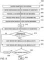
- One embodiment includes a method for manufacturing waveguide cells, the method including providing a first substrate, determining a predefined grating characteristic, and depositing a layer of optical recording material onto the first substrate using at least one deposition head, wherein the optical recording material deposited over the grating region is formulated to achieve the predefined grating characteristic.
- the method further includes providing a second substrate, placing the second substrate onto the deposited layer of optical recording material, and laminating the first substrate, the layer of optical recording material, and the second substrate.
- depositing the layer of optical recording material includes providing a first mixture of optical recording material, providing a second mixture of optical recording material, and depositing the first and second mixtures of optical recording material onto the first substrate in a predetermined pattern using the at least one deposition head.
- the first mixture of optical recording material includes a first bead and the second mixture of optical recording material includes a second bead that is a different size from the first bead.
- the first mixture of optical recording material has a different percentage by weight of liquid crystals than the second mixture of optical recording material.
- the method further includes defining a grating region and a nongrating region on the first substrate, wherein the first mixture of optical recording material includes a liquid crystal and a monomer, the second mixture of optical recording material includes a monomer, and depositing the first and second mixtures of optical recording material onto the first substrate in the predetermined pattern includes depositing the first mixture of optical recording material over the grating region and depositing the second mixture of optical recording material over the nongrating region.
- the first mixture of optical recording material is a polymer dispersed liquid crystal mixture that includes a monomer, a liquid crystal, a photoinitiator dye, and a coinitiator.
- the polymer dispersed liquid crystal mixture includes an additive selected from the group that includes a photoinitiator, nano particles, low-functionality monomers, additives for reducing switching voltage, additives for reducing switching time, additives for increasing refractive index modulation, and additives for reducing haze.
- the at least one deposition head includes at least one inkjet print head.
- depositing the layer of optical recording material includes providing a first mixture of optical recording material, providing a second mixture of optical recording material, printing a first dot of the first mixture of optical recording material using the at least one inkjet print head, and printing a second dot of the second mixture of optical recording material adjacent to the first dot using the at least one inkjet print head.
- the at least one inkjet print head includes a first inkjet print head and a second inkjet print head and depositing the layer of optical recording material includes providing a first mixture of optical recording material, providing a second mixture of optical recording material, printing the first mixture of optical recording material onto the first substrate using the first inkjet print head, and printing the second mixture of optical recording material onto the first substrate using the second inkjet print head.
- the predefined grating characteristic includes a characteristic selected from the group that includes refractive index modulation, refractive index, birefringence, liquid crystal director alignment, and grating layer thickness.
- the predefined grating characteristic includes a spatial variation of a characteristic selected from the group that includes refractive index modulation, refractive index, birefringence, liquid crystal director alignment, and grating layer thickness.
- the predefined grating characteristic results in a grating after exposure, wherein the grating has a spatially varying diffraction efficiency.
- a still further additional embodiment includes a system for fabricating a grating, the system including at least one deposition head connected to at least one reservoir containing at least one mixture of optical recording material, a first substrate having at least one predefined region for supporting gratings, a positioning element capable of positioning the at least one deposition head across the first substrate, wherein the at least one deposition head is configured to deposit the at least one mixture of optical recording material onto the first substrate using the positioning element and the deposited material provides a predefined grating characteristic within the at least one predefined grating region after holographic exposure.
- the at least one deposition head is connected to a first reservoir containing a first mixture of optical recording material and a second reservoir containing a second mixture of optical recording material.
- the first mixture of optical recording material includes a liquid crystal and a monomer and the second mixture of optical recording material includes a monomer, wherein the at least one deposition head is configured to deposit the first mixture of optical recording material onto the at least one predefined grating region.
- the at least one deposition head includes at least one inkjet print head.
- the predefined grating characteristic includes a characteristic selected from the group that includes refractive index modulation, refractive index, birefringence, liquid crystal director alignment, and grating layer thickness.
- the predefined grating characteristic results in a grating after exposure, wherein the grating has a spatially varying diffraction efficiency.
- the term "on-axis" in relation to a ray or a beam direction refers to propagation parallel to an axis normal to the surfaces of the optical components described in relation to the invention.
- the terms light, ray, beam and direction may be used interchangeably and in association with each other to indicate the direction of propagation of light energy along rectilinear trajectories. Parts of the following description will be presented using terminology commonly employed by those skilled in the art of optical design. For illustrative purposes, it is to be understood that the drawings are not drawn to scale unless stated otherwise.
- a waveguide cell can be defined as a device containing uncured and/or unexposed optical recording material in which optical elements, such as but not limited to gratings, can be recorded through exposure to certain wavelengths of electromagnetic radiation.
- optical elements such as but not limited to gratings
- a waveguide cell is constructed by placing a thin film of optical recording material between two transparent substrates.
- a workcell cluster manufacturing system is implemented to construct such waveguide cells.
- a workcell can be defined as a set of machines assigned to a particular manufacturing task.
- a cluster can be defined as a group of machines that performs a similar function cooperatively.
- the workcell cluster includes a preparation workcell for preparing substrates for deposition, a deposition workcell for depositing an optical recording material onto a substrate, and a lamination workcell for laminating various layers together to form a waveguide cell.
- preparation workcells can be configured to prepare substrates for material deposition through various processes, including but not limited to cleaning procedures and protocols.
- the preparation of substrates includes glass cleaning procedures for ridding the surfaces of the substrates of contaminants and particles.
- procedures for increasing the surface adhesion properties of the substrates are implemented to further prepare the substrates for material deposition.
- Deposition workcells can be configured to deposit one or more layers of optical recording material onto a transparent substrate using a variety of different deposition and printing mechanisms.
- additive manufacturing techniques such as but not limited to inkjet printing, are used to deposit the layer(s) of optical recording material.
- spraying techniques are utilized to deposit the layer(s) of optical recording material.
- Suitable optical recording material can vary widely depending on the given application.
- the optical recording material deposited has a similar composition throughout the layer.
- the optical recording material spatially varies in composition, allowing for the formation of optical elements with varying characteristics. Regardless of the composition of the optical recording material, any method of placing or depositing the optical recording material onto a substrate can be utilized.
- Lamination workcells can be configured to laminate various layers to form a waveguide cell.
- the lamination workcell is configured to laminate and form a three-layer composite of optical recording material and transparent substrates.
- the number of layers and types of materials used to construct the waveguide cells can vary and depend on the given application.
- waveguide cells can be constructed to include protective cover layers, polarization control layers, and/or alignment layers.
- the system is configured for the production of curved waveguides and waveguide cells. Specific materials, systems, and methods for constructing waveguide cells are discussed below in further detail.
- Waveguide cells can be configured and constructed in many different ways in accordance with various embodiments of the invention.
- the waveguide cell includes a thin film of optical recording material sandwiched between two substrates.
- Such waveguide cells can be manufactured using various processes.
- waveguide cells can be constructed by coating a first substrate with an optical recording material capable of acting as an optical recording medium.
- the optical recording material is a holographic polymer dispersed liquid crystal mixture (e.g., a matrix of liquid crystal droplets).
- the choice of optical recording material and types of mixtures utilized can depend on the given application.
- the optical recording material can be deposited using a variety of deposition techniques.
- the optical recording material can be deposited onto the first substrate through inkjetting, spin coating, and/or spraying processes.
- the deposition processes can be configured to deposit one or more type of optical recording material.
- the deposition process is configured to deposit optical recording material that spatially varies in composition across a substrate.
- a second substrate can be placed such that the optical recording material is sandwiched between the two substrates to form a waveguide cell.
- the second substrate can be a thin protective film coated onto the exposed layer.
- various techniques including but not limited to spraying processes, can be used to coat the exposed layer with the desired film of material.
- the waveguide cell can include various additional layers, such as but not limited to polarization control layers and/or alignment layers.
- Other processes for manufacturing waveguide cells can include filling empty waveguide cells (constructed of two substrates) with an optical recording material using processes such as but not limited to gravity filling and vacuum filling methods.
- Substrates used in the construction of waveguide cells are often made of transparent materials.
- the substrate is an optical plastic.
- the substrate may be fabricated from glass.
- An exemplary glass substrate is standard Corning Willow glass substrate (index 1.51) which is available in thicknesses down to 50 micrometers. The thicknesses of the substrates can vary from application to application. In many embodiments, 1 mm thick glass slides are used as the substrates.
- substrates of different shapes such as but not limited to rectangular and curvilinear shapes, can also be used depending on the application. Oftentimes, the shapes of the substrates can determine the overall shape of the waveguide.
- the waveguide cell contains two substrates that are of the same shape. In other embodiments, the substrates are of different shapes. As can readily be appreciated, the shapes, dimensions, and materials of the substrates can vary and depend on the specific requirements of a given application.
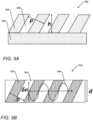
- beads or other particles are dispersed throughout the optical recording material to help control the thickness of the layer of optical recording material and to help prevent the two substrates from collapsing onto one another.
- the waveguide cell is constructed with an optical recording material layer sandwiched between two planar substrates. Depending on the type of optical recording material used, thickness control can be difficult to achieve due to the viscosity of some optical recording materials and the lack of a bounding edge for the optical recording material layer.
- the beads are relatively incompressible solids, which can allow for the construction of waveguide cells with consistent thicknesses. The size of a bead can determine a localized minimum thickness for the area around the individual bead.
- the dimensions of the beads can be selected to help attain the desired optical recording material layer thickness.
- the beads can be made of any of a variety of materials, including but not limited to glass and plastics.
- the material of the beads is selected such that its refractive index does not substantially affect the propagation of light within the waveguide cell.
- the waveguide cell is constructed such that the two substrates are parallel or substantially parallel. In such embodiments, relatively similar sized beads can be dispersed throughout the optical recording material to help attain a uniform thickness throughout the layer.
- the waveguide cell has a tapered profile.
- a tapered waveguide cell can be constructed by dispersing beads of different sizes across the optical recording material. As discussed above, the size of a bead can determine the local minimum thickness of the optical recording material layer. By dispersing the beads in a pattern of increasing size across the material layer, a tapered layer of optical recording material can be formed when the material is sandwiched between two substrates.
- waveguide cells can be used in conjunction with a variety of processes for recording optical elements within the optical recording material.
- the process disclosed may incorporated embodiments and teachings from the materials and processes, such as but not limited to those described in U.S. Patent Application No. 16/116,834 entitled “Systems and Methods for High-Throughput Recording of Holographic Gratings in Waveguide Cells," filed August 29, 2018 and U.S. Patent Application No. 16/007,932 entitled “Holographic Material Systems and Waveguides Incorporating Low Functionality Monomers,” filed June 13, 2018
- the disclosures of U.S. Patent Application Nos. 16/116,834 and 16/007,932 are hereby incorporated in their entireties for all purpose.
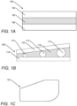
- FIG. 1A A profile view of a waveguide cell 100 in accordance with an embodiment of the invention is conceptually illustrated in FIG. 1A .
- the waveguide cell 100 includes a layer of optical recording material 102 that can be used as a recording medium for optical elements, such as but not limited to gratings.
- the optical recording material 102 can be any of a variety of compounds, mixtures, or solutions, such as but not limited to the HPDLC mixtures described in the sections above.
- the optical recording material 102 is sandwich between two parallel glass plates 104, 106.
- the substrates can be arranged in both parallel and non-parallel configurations.
- FIG. 1A A profile view of a waveguide cell 100 in accordance with an embodiment of the invention is conceptually illustrated in FIG. 1A .
- the waveguide cell 100 includes a layer of optical recording material 102 that can be used as a recording medium for optical elements, such as but not limited to gratings.
- the optical recording material 102 can be any of a variety of compounds,
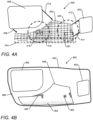
- FIG. 1B conceptually illustrates a profile view of a tapered waveguide cell 108 utilizing beads 110, 112, and 114 in accordance with an embodiment of the invention.
- beads 110, 112, and 114 vary in size and are dispersed throughout an optical recording material 116 sandwiched by two glass plates 118, 120.
- the local thickness of an area of the optical recording material layer is limited by the sizes of the beads in that particular area.
- a tapered waveguide cell can be constructed when the substrates are placed in contact with the beads.
- substrates utilized in waveguide cells can vary in thicknesses and shapes. In many embodiments, the substrate is rectangular in shape.
- the shape of the waveguide cell is a combination of curvilinear components.
- FIG. 1C conceptually illustrates a top view of a waveguide cell 122 having a curvilinear shape in accordance with an embodiment of the invention.
- FIGs. 1A - 1C illustrate specific waveguide cell constructions and arrangements, waveguide cells can be constructed in many different configurations and can use a variety of different materials depending on the specific requirements of a given application.
- substrates can be made of transparent plastic polymers instead of glass.
- the shapes and sizes of the waveguide cells can vary greatly and can be determined by various factors, such as but not limited to the application of the waveguide, ergonomic considerations, and economical factors.
- the substrates are curved, allowing for the production of waveguides with curved cross sections.
- Waveguide cells in accordance with various embodiments of the invention can incorporate a variety of light-sensitive materials.
- the waveguide cell incorporates a holographic polymer dispersed liquid crystal mixture that functions as an optical recording medium in which optical elements can be recorded.
- Optical elements can include many different types of gratings capable of exhibiting different optical properties.
- One type of grating that can be recorded in waveguide cells is a volume Bragg grating, which can be characterized as a transparent medium with a periodic variation in its refractive index. This variation can allow for the diffraction of incident light of certain wavelengths at certain angles.
- Volume Bragg gratings can have high efficiency with little light being diffracted into higher orders. The relative amount of light in the diffracted and zero order can be varied by controlling the refractive index modulation of the grating.
- SBG Switchable Bragg Grating
- An SBG is a diffractive device that can be formed by recording a volume phase grating in an HPDLC mixture (although other materials can be used).
- SBGs can be fabricated by first placing a thin film of a mixture of photopolymerizable monomers and liquid crystal material between glass plates or substrates, which forms a waveguide cell.
- One or both glass plates can support electrodes, typically transparent tin oxide films, for applying an electric field across the film.
- SBGs can be implemented as waveguide devices in which the HPDLC forms either the waveguide core or an evanescently coupled layer in proximity to the waveguide.
- the glass plates used to form the HPDLC cell can provide a total internal reflection light guiding structure. Light is coupled out of the SBG when the switchable grating diffracts the light at an angle beyond the TIR condition.
- the grating structure in an SBG can be recorded in the film of HPDLC material through photopolymerization-induced phase separation using interferential exposure with a spatially periodic intensity modulation. Factors such as but not limited to control of the irradiation intensity, component volume fractions of the HPDLC material, and exposure temperature can determine the resulting grating morphology and performance.
- the monomers polymerize and the mixture undergoes a phase separation.
- the LC molecules aggregate to form discrete or coalesced droplets that are periodically distributed in polymer networks on the scale of optical wavelengths.
- the alternating liquid crystal-rich and liquid crystal-depleted regions form the fringe planes of the grating, which can produce Bragg diffraction with a strong optical polarization resulting from the orientation ordering of the LC molecules in the droplets.
- the resulting volume phase grating can exhibit very high diffraction efficiency, which may be controlled by the magnitude of the electric field applied across the HPDLC layer.
- an electric field is applied to the hologram via transparent electrodes, the natural orientation of the LC droplets is changed, causing the refractive index modulation of the fringes to reduce and the hologram diffraction efficiency to drop to very low levels.
- the diffraction efficiency of the device can be adjusted, by means of the applied voltage, over a continuous range from near 100% efficiency with no voltage applied to essentially zero efficiency with a sufficiently high voltage applied.
- phase separation of the LC material from the polymer can be accomplished to such a degree that no discernible droplet structure results.
- An SBG can also be used as a passive grating. In this mode, its chief benefit is a uniquely high refractive index modulation.
- SBGs can be used to provide transmission or reflection gratings for free space applications.
- SBGs can be implemented as waveguide devices in which the HPDLC forms either the waveguide core or an evanescently coupled layer in proximity to the waveguide.
- the glass plates used to form the HPDLC cell provide a total internal reflection light guiding structure. Light can be coupled out of the SBG when the switchable grating diffracts the light at an angle beyond the TIR condition.
- SBGs are recorded in a uniform modulation material, such as POLICRYPS or POLIPHEM having a matrix of solid liquid crystals dispersed in a liquid polymer.
- a uniform modulation material such as POLICRYPS or POLIPHEM having a matrix of solid liquid crystals dispersed in a liquid polymer.
- Exemplary uniform modulation liquid crystal-polymer material systems are disclosed in United State Patent Application Publication No.: US2007/0019152 by Caputo et al and PCT Application No.: PCT/EP2005/006950 by Stumpe et al. both of which are incorporated herein by reference in their entireties.
- Uniform modulation gratings are characterized by high refractive index modulation (and hence high diffraction efficiency) and low scatter.
- at least one of the gratings is recorded a reverse mode HPDLC material.
- Reverse mode HPDLC differs from conventional HPDLC in that the grating is passive when no electric field is applied and becomes diffractive in the presence of an electric field.
- the reverse mode HPDLC may be based on any of the recipes and processes disclosed in PCT Application No.: PCT/GB2012/000680 , entitled IMPROVEMENTS TO HOLOGRAPHIC POLYMER DISPERSED LIQUID CRYSTAL MATERIALS AND DEVICES. Optical recording material systems are discussed below in further detail.
- HPDLC mixtures in accordance with various embodiments of the invention generally include LC, monomers, photoinitiator dyes, and coinitiators.
- the mixture (often referred to as syrup) frequently also includes a surfactant.
- a surfactant is defined as any chemical agent that lowers the surface tension of the total liquid mixture.
- the use of surfactants in PDLC mixtures is known and dates back to the earliest investigations of PDLCs. For example, a paper by R.L Sutherland et al., SPIE Vol.
- polymer-dispersed liquid crystal material for forming a polymer-dispersed liquid crystal optical element including: at least one acrylic acid monomer; at least one type of liquid crystal material; a photoinitiator dye; a coinitiator; and a surfactant.
- the disclosure of U.S. Patent No. 7,018,563 is hereby incorporated by reference in its entirety.
- Acrylates offer the benefits of fast kinetics, good mixing with other materials, and compatibility with film forming processes. Since acrylates are cross-linked, they tend to be mechanically robust and flexible. For example, urethane acrylates of functionality 2 (di) and 3 (tri) have been used extensively for HPDLC technology. Higher functionality materials such as penta and hex functional stems have also been used.
- HPDLC mixtures with specific components are discussed above in relation with their suitable uses as the optical recording material in a waveguide cell
- specific formulations of optical recording materials can vary widely and can depend on the specific requirements of a given application. Such considerations can include diffraction efficiency ("DE”), haze, solar immunity, transparency, and switching requirements.
- DE diffraction efficiency
- the S and P polarization response of a grating containing LC can depend on the average LC director orientations relative to the grating K-vector.
- the directors are substantially parallel to the K-vector, giving a strong P-response and a weaker S-response. If the LC directors are not aligned, the grating can have a strong S-response.
- RLCM reactive monomer liquid crystal mixture
- monomers and other components including: photoinitiator dye, coinitiators, surfactant
- photoinitiator dye coinitiators
- surfactant which under holographic exposure undergo phase separation to provide a grating in which at least one of the LCs and at least one of the monomers form a first HPDLC morphology that provides a P polarization response and at least one of the LCs and at least one of the monomers form a second HPDLC morphology that provides a S polarization response.
- the material systems include an RMLCM, which includes photopolymerizable monomers composed of suitable functional groups (e.g., acrylates, mercapto-, and other esters, among others), a cross-linking agent, a photo-initiator, a surfactant and a liquid crystal.
- suitable functional groups e.g., acrylates, mercapto-, and other esters, among others
- cross-linking agent e.g., acrylates, mercapto-, and other esters, among others
- surfactant e.g., acrylates, mercapto-, and other esters, among others
- any encapsulating polymer formed from any single photo-reactive monomer material or mixture of photo-reactive monomer materials having refractive indices from about 1.5 to 1.9 that crosslink and phase separate when combined can be utilized.
- Exemplary monomer functional groups usable in material formulations according to embodiments include, but are not limited to, acrylates, thiol-ene, thiol-ester, fluoromonomers, mercaptos, siloxane-based materials, and other esters, etc.
- Polymer cross-linking can be achieved through different reaction types, including but not limited to optically-induced photo-polymerization, thermally-induced polymerization, and chemically-induced polymerization.
- photopolymerizable materials can be combined in a biphase blend with a second liquid crystal material.
- a second liquid crystal material Any suitable liquid crystal material having ordinary and extraordinary refractive indices matched to the polymer refractive index can be used as a dopant to balance the refractive index of the final RMLCM material.
- the liquid crystal material can be manufactured, refined, or naturally occurring.
- the liquid crystal material includes all known phases of liquid crystallinity, including the nematic and smectic phases, the cholesteric phase, the lyotropic discotic phase.
- the liquid crystal can exhibit ferroelectric or antiferroelectric properties and/or behavior.
- any suitable photoinitiator, co-initiator, chain extender and surfactant (such as for example octanoic acid) suitable for use with the monomer and LC materials can be used in the RMLCM material formulation. It will be understood that the photo-initiator can operate in any desired spectral band including the in the UV and/or in the visible band.
- the LCs can interact to form an LC mixture in which molecules of two or more different LCs interact to form a non-axial structure which interacts with both S and P polarizations.
- the waveguide can also contain an LC alignment material for optimizing the LC alignment for optimum S and P performance.
- the ratio of the diffraction efficiencies of the P- and S-polarized light in the PDLC morphology is maintained at a relative ratio of from 1.1:1 to 2:1, and in some embodiments at around 1.5:1.
- the measured diffraction efficiency of P-polarized light is from greater than 20% to less than 60%, and the diffraction efficiency for S-polarized light is from greater than 10% to less than 50%, and in some embodiments the diffraction efficiency of the PDLC morphology for P-polarization is around 30% and the diffraction efficiency of the PDLC morphology for S-polarization is around 20%.
- This can be compared with conventional PDLC morphologies where the diffraction efficiency for P-polarization is around 60% and for S-polarization is around 1% (i.e., the conventional P-polarization materials have very low or negligible S-components).
- the reactive monomer liquid crystal mixture can further include chemically active nanoparticles disposed within the LC domains.
- the nanoparticles are carbon nanotube ("CNT") or nanoclay nanoparticle materials within the LC domains.
- CNT carbon nanotube
- Embodiments are also directed to methods for controlling the nanoclay particle size, shape, and uniformity. Methods for blending and dispersing the nanoclay particles can determine the resulting electrical and optical properties of the device. The use of nanoclays in HPDLC is discussed in PCT Application No.: PCT/GB2012/000680 , entitled IMPROVEMENTS TO HOLOGRAPHIC POLYMER DISPERSED LIQUID CRYSTAL MATERIALS AND DEVICES.
- the nanoclay nanoparticles can be formed from any naturally occurring or manufactured composition, as long as they can be dispersed in the liquid crystal material.
- the specific nanoclay material to be selected depends upon the specific application of the film and/or device.
- the concentration and method of dispersion also depends on the specific application of the film and/or device.
- the liquid crystal material is selected to match the liquid crystal ordinary index of refraction with the nanoclay material.
- the resulting composite material can have a forced alignment of the liquid crystal molecules due to the nanoclay particle dispersion, and the optical quality of the film and/or device can be unaffected.
- the composite mixture which includes the liquid crystal and nanoclay particles, can be mixed to an isotropic state by ultrasonication.
- the mixture can then be combined with an optically crosslinkable monomer, such as acrylated or urethane resin that has been photoinitiated, and sandwiched between substrates to form a cell (or alternatively applied to a substrate using a coating process).
- nanoparticles are composed of nanoclay nanoparticles, preferably spheres or platelets, with particle size on the order of 2-10 nanometers in the shortest dimension and on the order of 10 nanometers in the longest dimension.
- the liquid crystal material is selected to match the liquid crystal ordinary index of refraction with the nanoclay material.
- the nanoparticles can be composed of material having ferroelectric properties, causing the particles to induce a ferroelectric alignment effect on the liquid crystal molecules, thereby enhancing the electro-optic switching properties of the device.
- the nanoparticles are composed of material having ferromagnetic properties, causing the particles to induce a ferromagnetic alignment effect on the liquid crystal molecules, thereby enhancing the electro-optic switching properties of the device.
- the nanoparticles have an induced electric or magnetic field, causing the particles to induce an alignment effect on the liquid crystal molecules, thereby enhancing the electro-optic switching properties of the device.
- Exemplary nanoparticles used in other contexts including thermoplastics, polymer binders, etc. are disclosed in U.S. Patent Nos. 7,068,898 ; 7,046,439 ; 6,323,989 ; 5,847,787 ; and U.S. Patent Pub. Nos. 2003/0175004 ; 2004/0156008 ; 2004/0225025 ; 2005/0218377 ; and 2006/0142455 , the disclosures of which are incorporated herein by reference.
- the nanoclay can be used with its naturally occurring surface properties, or the surface can be chemically treated for specific binding, electrical, magnetic, or optical properties.
- the nanoclay particles will be intercalated, so that they disperse uniformly in the liquid crystalline material.
- the generic term "nanoclay" as used in the discussion of the present invention can refer to naturally occurring montmorillonite nanoclay, intercalated montmorillonite nanoclay, surface modified montmorillonite nanoclay, and surface treated montmorillonite nanoclay.
- the nanoparticles can be useable as commercially purchased, or they may need to be reduced in size or altered in morphology.
- the processes that can be used include chemical particle size reduction, particle growth, grinding of wet or dry particles, milling of large particles or stock, vibrational milling of large particles or stock, ball milling of particles or stock, centrifugal ball milling of particles or stock, and vibrational ball milling of particles or stock. All of these techniques can be performed either dry or with a liquid suspension.
- the liquid suspension can be a buffer, a solvent, an inert liquid, or a liquid crystal material.
- Spex LLC Metaluchen, NJ
- Retsch France
- the nanoparticles can be dispersed in the liquid crystal material prior to polymer dispersion. Dry or solvent suspended nanoparticles can be ultrasonically mixed with the liquid crystal material or monomers prior to polymer dispersion to achieve an isotropic dispersion. Wet particles may need to be prepared for dispersion in liquid crystal, depending on the specific materials used. If the particles are in a solvent or liquid buffer, the solution can be dried, and the dry particles dispersed in the liquid crystal as described above. Drying methods include evaporation in air, vacuum evaporation, purging with inert gas like nitrogen and heating the solution.
- the optical film includes a liquid crystal material and a nanoclay nanoparticle, where a nanoparticle is a particle of material with size less than one micrometer in at least one dimension.
- the film can be isotropically distributed.
- CNT is used as an alternative to nanoclay as a means for reducing voltage.
- the properties of CNT in relation to PDLC devices are reviewed by E.H. Kim et. al. in Polym. Int. 2010; 59: 1289- 1295 , the disclosure of which is incorporated herein by reference in its entirety.
- PDLC films have been fabricated with varying amounts of multi- walled carbon nanotubes ("MWCNTs") to optimize the electro-optical performance of the PDLC films.
- MWCNTs multi- walled carbon nanotubes
- the MWCNTs were well dispersed in the prepolymer mixture up to 0.5 wt%, implying that polyurethane acrylate ("PUA") oligomer chains wrap the MWCNTs along their length, resulting in high diffraction efficiency and good phase separation.
- PUA polyurethane acrylate
- the hardness and elastic modulus of the polymer matrix were enhanced with increasing amounts of MWCNTs because of the reinforcement effect of the MWCNTs with intrinsically good mechanical properties.
- the increased elasticity of the PUA matrix and the immiscibility between the matrix and the liquid crystals gradually increased the diffraction efficiency of the PDLC films.
- PDLC films with more than 0.05 wt% MWCNTs were reduced, caused by poor phase separation between the matrix and LCs because of the high viscosity of the reactive mixture.
- PDLC films showing a low driving voltage (75%) could be obtained with 0.05 wt% MWCNTs at 40 wt% LCs.
- the PDLC materials incorporate such nanoparticles
- reductions of switching voltage and improvements to the electro-optic properties of a polymer dispersed liquid crystal film and/or polymer dispersed liquid crystal device can be obtained by including nanoparticles in the liquid crystal domains.
- the inclusion of nanoparticles serves to align the liquid crystal molecules and to alter the birefringent properties of the film through index of refraction averaging.
- the inclusion of the nanoparticles improves the switching response of the liquid crystal domains.
- the material system is an RMLCM that includes at least one LC, at least one multi-functional monomer, a photo-initiator, a dye, and at least one mono-functional monomer.
- the specific mixture of components and their percent composition can determine the diffraction efficiency of the resulting HPDLC gratings.
- Inhomogeneous polymerization due to the spatially periodic irradiation intensity of the exposure can be the driving force to segregate monomers and LCs and to order the orientation of LC molecules, which can influence the diffraction efficiencies of the HPDLC gratings.
- the diffusion coefficient of monomers depends on their molecular weight and reactivity. It has been shown that a variety of monomer molecular weights or functional numbers can yield a complex distribution of polymer and LC phases. In many cases, molecular functionality can be critical in achieving efficient phase separation and the formation of gratings with high diffraction efficiency.
- many embodiments of the invention include material systems formulated with specific mixes of monomers that are chosen, at least in part, for their functionality so as to influence the diffraction efficiency and index modulation of the resulting grating structure.
- Other considerations in formulating such a mixture can include but are not limited to the properties of the recording beam and the thickness of the gratings.
- the functionality of a monomer refers to the number of reactive sites on each monomer unit.
- the monomers within the mixture are either mono-functional monomers or bi-functional monomers.
- tri-functional monomers are also included. In such mixtures, the tri-functional monomers are typically included at a low concentration, such as lower than 5wt%.
- Mixtures including low functional monomers can behave differently depending on a variety of factors, such as but not limited to the wavelength sensitivity of the material system, thickness of the HPDLC to be formed, and exposure temperature.
- investigations into PDLC material systems typically include UV sensitive material systems since material reaction efficiency in general is typically poor with visible light systems.
- formulations in accordance with various embodiments of the invention have been able to reach high diffraction efficiency (>80%) with low haze using low functionality monomers that are sensitive (polymerizes) to visible light.
- the material systems include monomers that are sensitive to green light, such as light with wavelengths ranging from 495-570 nm.
- the material system is formulated for use in waveguides with thin form factors.
- the material system is formulated for use in manufacturing waveguides having HPDLC layers with thicknesses of less than 10 ⁇ m. and gratings with more than 80% diffraction efficiency.
- the material system is formulated for use in a waveguide having a 2-3 ⁇ m thick HPDLC layer and gratings with 80-90% diffraction efficiency.
- the material system can also be formulated for manufacturing such waveguides with low haze.
- the material system can form HPDLC layers having less than 1% haze.
- Waveguide haze is the integrated effect of light interacting with material and surface inhomogeneities over many beam bounces. The impact on the ANSI contrast, the ratio of averaged white to black measurements taken from a checkerboard pattern, can be dramatic owing to the scatter contribution to the black level.
- Haze is mostly due to wide-angle scatter by LC droplets and other small particles or scattering centers resulting from incomplete phase separation of the LC/monomer mixture during grating recording. Haze can also arise, at least partly, from narrow angle scatter generated by large-scale nonuniformities, leading to a loss of see-through quality and reduced image sharpness.
- Some waveguide applications such as aircraft HUDs, which use 1-D beam expansion in thick waveguides, produce as few as 7 bounces, allowing up to 80:1 contrast.
- the number of bounces may increase by a factor of 10 making the need for haze control more acute.
- RMLCM recipes can be optimized for specific thicknesses of HPDLC layers.
- the RMLCM recipe is optimized for a ⁇ 3 ⁇ m thick uniform modulation gratings designed to have a refractive index modulation of -0.16.
- the specific thickness of the waveguide parts to be fabricated can vary and can depend on the specific requirements of a given application.
- the waveguide parts can be fabricated with 90% transmission and 0.3% haze.
- the waveguide parts can be fabricated with -0.1% haze (with -0.01% haze recorded in unexposed samples of the same material).
- the RMLCM can be formulated for fabricating waveguide parts containing haze of less than 0.05%.
- Transmission haze can be defined as the percentage of light that deviates from desired beam direction by more the 2.5 degrees on average (according to the ASTM D1003 standard).
- the clarity of a waveguide can be characterized by the amount of narrow angle scattered light (at an angle less than 2.5° from the normal to the waveguide surface). Transmission can be defined as the amount of light transmitted through the waveguide without being scattered.
- the scatter can be measured around a vector normal to a waveguide TIR surface.
- holographic haze the scatter can be measured around principal diffraction directions (passing through the center of the eye box).
- the RMLCM mixture includes a liquid crystal mixture, a complex mixture of acrylates and acrylate esters, Dynasylan ® MEMO, and photoinitiators.
- the RMLCM includes EHA and DFHA. Depending on the specific mix of components and their percent composition, the resulting grating can have vastly different characteristics.
- the proportion of LC by weight is greater than 30%. In further embodiments, the proportion of LC is greater than 35wt%.
- the mixture includes liquid crystal with high birefringence. In further embodiments, the high birefringence liquid crystal accounts for more than 20wt% of the mixture. In a number of embodiments, dye and photo-initiators account for less than 5wt% of the mixture.
- Nematic LC materials can provide a range of birefringence (which can translate to refractive index modulation).
- Low to medium birefringence typically covers the range of 0.09 - 0.12.
- gratings can be designed using much lower birefringence values, including gratings in which the birefringence varies along the grating. Such gratings can be used to extract light from waveguides with low efficiency at one end of the grating and high efficiency at the other end of the grating to provide spatially uniform output illumination.
- High birefringence is typically the range of 0.2 - 0.5. Even higher values are possible.
- Nematic liquid crystals, compounds, and mixtures with positive dielectric anisotropies i.e., LCs for which the dielectric constant is greater in the long molecular axis than that in the other directions
- LCs for which the dielectric constant is greater in the long molecular axis than that in the other directions
- the mixture includes at least one mono-functional monomer and at least one multifunctional monomer in varying concentrations.
- the concentration of mono-functional monomer within the mixture ranges from 1 - 50wt%.
- the monofunctional monomer can include aliphatic/aromatic groups and an adhesion promoter.
- the proportion of multi-functional monomers present in the mixture is in the range of 2 - 30wt%.
- Multi-functional monomers in accordance with various embodiments of the invention typically include monomers of low functionality.
- the mixture includes a bi-functional monomer at a low concentration.
- the mixture includes bi-functional monomers at less than 15wt%. Depending on the type and concentration of bi-functional monomer in the mixture, adequate phase separation and grating formation can occur.
- the mono-functional monomer, bi-functional monomer and LC have relative weight ratios of 30%, 14%, and 40%, which resulted in a formulation that allowed for the recording of gratings with a diffraction efficiency higher than 90% and an index modulation of around 0.12.
- percent composition of each component within an RMLCM can vary widely. Formulations of such material systems can be designed to achieve certain characteristics in the resulting gratings. In many cases, the RMLCM is formulated to have as high a diffraction efficiency as possible.
- Waveguide cell manufacturing systems in accordance with various embodiments of the invention can be implemented as workcell clusters. By compartmentalizing different manufacturing steps into workcells, modular systems can be implemented.
- a workcell cluster includes a preparation workcell for preparing substrates for material deposition, a deposition workcell for depositing an optical recording material onto a substrate, and a lamination workcell for laminating various layers together to construct a waveguide cell.
- Workcells can be configured in various ways to implement different manufacturing processes for waveguide cells. In some embodiments, the workcells are linked and configured such that the output of one workcell is transferred to another workcell, forming a manufacturing assembly line.
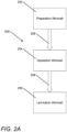
- FIG. 2A conceptually illustrates a workcell cluster system 200 in accordance with an embodiment of the invention.
- the system 200 includes a preparation workcell 202, a deposition workcell 204, and a lamination workcell 206.
- arrows 208 indicate a sequential workflow relationship among the workcells.
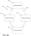
- FIG. 2B conceptually illustrates a workcell cluster system 210 with two deposition workcells 212, 214 in accordance with an embodiment of the invention.
- the system 210 includes a preparation workcell 216, two deposition workcells 212, 214, and a lamination workcell 218.
- Dotted arrows 220 indicate that output from the preparation workcell 216 can be received by either deposition workcell 212, 214. Such a system can be ideally implemented when the completion time for a single deposition process is approximately twice as long as the completion time for other processes.
- FIGs. 2A and 2B conceptually illustrate specific workcell cluster system configurations
- workcell clusters in accordance with various embodiments of the invention can be configured in numerous ways depending on the specific requirements of the given application.
- workcell clusters can be configured to have different workflow paths, types of workcells, and/or numbers of workcells.
- workcells can be configured to provide protection from environmental light and contaminants.
- optical filters cover the workcell in order to reduce and/or prevent unwanted light from interacting with the optical recording material, which is typically a photosensitive material.
- the deposition workcell can be lined with an appropriate optical filter that prevent light of certain wavelengths from entering the workcell and exposing the optical recording material.
- workcells can also be configured to reduce particulate contamination.
- the workcell is configured to operate in an environment with minimal air contamination. A low-particulate environment can be achieved in many different ways, including but not limited to the use of air filters.
- air filters employing laminar airflow principles are implemented.
- Contamination reduction/prevention systems such as those described above can be implemented separately or in combination.
- workcells in accordance with various embodiments of the invention can be constructed in various ways as to alter the working environment in a desired manner.
- the workcell is configured to operate in a vacuum. Specific workcells and their implementations and constructions are described in the sections below in further detail.
- Waveguide cells in accordance with various embodiments of the invention are typically composed of a layer of optical recording material sandwiched between two substrates.
- Manufacturing techniques for constructing such waveguide cells in accordance with various embodiments of the invention can include a deposition step where a layer of optical recording material is deposited onto one of the substrate.
- a preparation workcell can be implemented to perform a cleaning/preparation procedure on the substrates to prepare them for the deposition step.
- Preparing substrates such as but not limited to glass plates, can include ridding the surfaces of contaminants and increasing the surface adhesion properties for better material deposition.
- Preparation workcells can be configured to implement various cleaning and preparation protocols. Mechanical arms and/or suction apparatuses can be used to maneuver the substrates throughout the workcell.
- the preparation workcells are configured to clean glass substrates using various solvents and solutions, including but not limited to soap solutions, acid washes, acetone, and various types of alcohols.
- solvents and solutions are used in conjunction.
- methanol or isopropanol can be administered after acetone to rinse off excess acetone.
- deionized water is used to rinse off excess solvents or solutions.
- the solvents can be administered in several ways, including but not limited to the use of nozzles and baths.
- the workcell can be configured to dry the substrates using an inert gas, such as nitrogen, and/or a heating element.
- the cleaning process includes a sonication step.
- the substrate is placed in a chamber containing a solution and a transducer is used to produce ultrasonic waves.
- the ultrasonic waves can agitate the solution and remove contaminants adhered to the substrates.
- the treatment can vary in duration depending on several factors and can be performed with different types of substrates. Deionized water or cleaning solutions/solvents can be used depending on the type of contamination and the type of substrate.
- the preparation workcell is configured to implement a plasma chamber to plasma treat the surfaces of the substrates.
- the substrates are made of glass.
- Existing in the form of ions and electrons, plasma is essentially an ionized gas that has been electrified with extra electrons in both negative and positive states.
- Plasma can be used to treat the surface of the substrate to remove contaminants and/or prepare the surface for material deposition by increasing the surface energy to improve adhesion properties.
- the workcell includes a vacuum pump, which can be used to create a vacuum under which the plasma treatment can be performed.
- preparation workcells in accordance with various embodiments of the invention can be configured to perform combinations of various steps to implement a specific cleaning protocol according to the requirements of a given application.
- specific preparation workcells for preparing glass plates are discussed above, preparation workcells can be implemented to preform various preparatory steps for a variety of different substrates, including but not limited to plastics.
- Waveguide cell manufacturing systems can utilize various techniques for placing optical recording materials in between two substrates.
- Manufacturing systems in accordance with various embodiments of the invention can utilize a deposition process where a film of optical recording material is deposited onto a substrate, and the composite is laminated along with a second substrate to form a three-layer laminate.
- the manufacturing system is a workcell cluster that includes a deposition workcell for depositing a film of optical recording material onto a substrate.
- Such deposition workcells can be configured to receive substrates from preparation workcells.
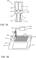
- the deposition workcell includes a stage for supporting the substrate and at least one deposition mechanism for depositing material onto the substrate. Any of a variety of deposition heads can be implemented to perform as the deposition mechanism.
- spraying mechanisms such as but not limited to spraying nozzles are implemented to deposit optical recording material onto a substrate.
- the optical recording material is deposited using a printing mechanism.
- the deposition head can allow for the deposition of different materials and/or mixtures that vary in component concentrations.
- the specific deposition mechanism utilized can depend on the specific requirements of a given application.
- the components within the deposition workcell can be configured to move in various ways in order to deposit the optical recording material onto the substrate.
- the deposition head and/or the stage are configured to move across certain axes in order to deposit one or multiple layers of optical recording material.
- the deposition head is configured to move and deposit material across three dimensions, such as in a three-dimensional Euclidean space, which allows for the deposition of multiple layers onto the substrate.
- the deposition head is only configured to move in two axes to deposit a single layer.
- the stage and, consequently, the substrate are configured to move in three dimensions while the deposition head is stationary.
- deposition applications can be implemented to deposit material in various dimensions by configuring the degrees of motion freedom of the print head(s) and/or stage.
- the stage and deposition head can be configured such that their combination of degrees of motion freedom allows for depositing material in n-dimensional Euclidean space, where n is the desired dimension.
- the deposition head is configured to move back and forth to deposit material in one axis while the stage moves in a different axis, allowing for the deposition of material in a two-dimensional Euclidean plane.
- the stage is implemented using a conveyor belt.
- the system can be designed such that the conveyor belt receives the substrate from a different workcell, such as the preparation workcell. Once received, the conveyor system can move the substrate along as a deposition head deposits a layer of material onto the substrate. At the end of the conveyor path, the substrate can be delivered into another workcell.
- the deposition workcell includes an inkjet print head configured to deposit optical recording material onto the substrate.
- inkjet printing refers to a printing method that deposits a matrix of ink dots to form a desired image.
- an inkjet print head contains a large amount of small individual nozzles that can each deposit a dot of material.
- inkjet printing can be used to create complex patterns and structures with high precision due to the size and number of nozzles in a typical inkjet print head. Applying these principles to waveguide cell manufacturing applications, inkjet printing can be used to print a uniform or near-uniform, in terms of thickness and composition, layer of optical recording material.
- one or multiple layers of the optical recording material can be printed onto the substrate.
- Various optical recording materials such as those described in the sections above, can be used in conjunction with an inkjet print head.
- the printing system can be configured for use with various types of substrates.
- the choice of material to be printed and the substrates used can depend on the specific requirements of a given application. For instance, choices in material systems can be selected based on printing stability and accuracy. Other considerations can include but are not limited to viscosity, surface tension, and density, which can influence several factors such as but not limited to droplet formability and the ability to form layers of uniform thickness,
- FIG. 3A shows an isometric view of the deposition workcell 300 while FIG. 3B shows a top view of the same deposition workcell 300.
- the deposition workcell 300 is constructed with a frame that can hold optical glass filters to prevent particulate contamination and environmental light from exposing optical recording materials within the workcell 300.
- the workcell includes chambers 302, 304 for receiving substrates and outputting waveguide cells.
- the stage is implemented as a conveyor belt 306 that moves received substrates along one direction.
- the deposition workcell 300 further includes an inkjet printer 308 implemented as a deposition mechanism.
- the inkjet printer 308 is configured to print across a direction different from the movement of the conveyor belt 306, allowing for the deposition of a layer of optical recording material across the planar surface of the substrates. Additionally, the deposition workcell 300 implements a roller laminator 310 for laminating the printed layer and two substrates to construct a waveguide cell. The workcell 300 is also implemented as a glovebox with gloves 312 that allow for the manual manipulation of the devices within the workcell 300 while maintaining a clean environment.
- FIGs. 3A and 3B depict a specific deposition workcell configuration
- deposition workcells can be configured in many ways in accordance with various embodiments of the invention.
- the laminator can be implemented in a separate lamination workcell.
- automatic system configurations can be implemented.
- multiple inkjet print heads are used.
- spraying nozzles are used as the deposition mechanism.
- High luminance and excellent color fidelity are important factors in AR waveguide displays. In each case, high uniformity across the FOV can be essential.
- the fundamental optics of waveguides can lead to non-uniformities due to gaps or overlaps of beams bouncing down the waveguide. Further non-uniformities may arise from imperfections in the gratings and non-planarity of the waveguide substrates.
- SBGs there can exist a further issue of polarization rotation by birefringent gratings. The biggest challenge is the fold grating where there are millions of light paths resulting from multiple intersections of the beam with the grating fringes. Careful management of grating properties, particularly the refractive index modulation, can be utilized to overcome non-uniformity in accordance with various embodiments of the invention.
- the design can be exported to the deposition mechanism, with each target index modulation translating to a unique deposition setting for each spatial resolution cell on the substrate to be coated.
- the spatial pattern can be implemented to 30 micrometers resolution with full repeatability.
- FIGs. 4A and4B conceptually illustrate schematically the use of reverse ray tracing to compute a compensated index modulation pattern for coating in accordance with various embodiments of the invention.
- the procedure can determine the optimum usable area of the fold grating and the refractive index modulation variation across the fold grating needed to provide uniform illumination at the eye box.
- FIG. 4A shows a mathematical model of a basic waveguide architecture that includes an input grating 402, a fold grating that is divided up into a calculation mesh 404, and an output grating 406. By tracing rays from points across the eye box through the output grating and through the fold grating, the fold grating cells which contribute to the eyebox illumination for a given FOV direction can be identified.
- Reverse beam paths from the output grating are indicated by the rays 408-414.
- the maximum extent of the fold grating needed to fill the eye box can be determined. This ensures that the area of HPDLC material to be deposited/printed can be kept to a minimum, thereby reducing haze in the finished waveguide part.
- the procedure can also identify which cells need to have their index modulation increased (or decreased) in order to maintain illumination uniformity across the eyebox. For example, in the embodiment of FIG.4A , most of the fold grating region has a refractive index modulation of 0.03.
- FIG. 4B is a plan view 450 of the final waveguide part 452 onto which is superimposed the index modulation map of the printed grating layer (corresponding to the model of FIG.4A ) as would be revealed by examining the printed grating under cross polarizers.
- the grating regions include the input 454, output 456, and fold 458 gratings.
- the fold grating contains the high index modulation regions 460, 462, and 464 corresponding to the cells identified in regions 416, 420, and 424 of FIG.4A .
- the grating regions of FIG.4B are surrounded by a clear polymer region 466.
- FIGs. 4A and 4B illustrate a specific way of computing a compensated index modulation pattern, any of a variety of techniques can be utilized to compute such a pattern.
- SBG waveguides Compared with waveguides utilizing surface relief gratings ("SRGs"), SBG waveguides implementing manufacturing techniques in accordance with various embodiments of the invention can allow for the grating design parameters that impact efficiency and uniformity, such as refractive index modulation and grating thickness, to be adjusted dynamically during the deposition process. As such, there is no need for a new master for the grating recording process. With SRGs where modulation is controlled by etch depth, such schemes would not be practical as each variation of the grating would entail repeating the complex and expensive tooling process. Additionally, achieving the required etch depth precision and resist imaging complexity can be very difficult.
- FIGs. 5A and 5B conceptually illustrate the fundamental structural differences between SBGs and SRGs.
- FIG. 5A shows a cross-sectional view 500 of a portion of an SRG.
- the grating includes a substrate 502 supporting slanted surface relief elements 504 separated by air gaps 506.
- the surface relief elements and substrate are formed from a common material.
- the grating pitch is indicated by the symbol p and the grating depth by symbol h.
- FIG. 5B shows a cross-sectional view 550 of an SBG.
- the SBG includes alternating slanted Bragg fringes formed from low index monomer-rich fringes such as 552 and higher index LC-rich fringes such as 554.
- the index difference is characterized by the refractive index modulation ⁇ n , which plays an equivalent role in determining grating diffraction efficiency to the grating depth in a SRG.
- the variation of index modulation is represented by the superimposed plot 556 of index modulation versus distance z along the grating.
- the index modulation has a sinusoidal profile as shown in FIG. 5B .
- the index modulation profile can include near-rectangular LC-rich and polymer-rich regions.
- Deposition processes in accordance with various embodiments of the invention can provide for the adjustment of grating design parameters by controlling the type of material that is to be deposited. Similar to multi-material additive manufacturing techniques, various embodiments of the invention can be configured to deposit different materials, or different material compositions, in different areas on the substrate. In many embodiments, a layer of optical recording material can be deposited with different materials in different areas. For example, deposition processes can be configured to deposit HPDLC material onto an area of a substrate that is meant to be a grating region and to deposit monomer onto an area of the substrate that is meant to be a nongrating region.
- the deposition process is configured to deposit a layer of optical recording material that varies spatially in component composition, allowing for the modulation of various aspects of the deposited material. Modulation schemes and deposition processes for different types of materials and mixtures are discussed below in further detail.
- the deposition head is configured to deposit a layer of optical recording material for a waveguide cell intended to be recorded with three different gratings.
- the layer can be deposited such that the materials printed in each of the areas designated for the three gratings are all different from one another.
- FIG. 6 conceptually illustrates a waveguide cell 600 with marked areas intended to be recorded with various gratings in accordance with an embodiment of the invention. As shown, areas for an input grating 602, a fold grating 604, and an output grating 606 are outlined. Such areas can each be composed of a different material or different mixture composition depending on the given application.
- the waveguide cell is in a curvilinear shape, which, along with the positions, sizes, and shapes of the gratings, is designed to be a waveguide for near-eye applications.
- Deposition of material with different compositions can be implemented in several different ways.
- more than one deposition head can be utilized to deposit different materials and mixtures.
- Each deposition head can be coupled to a different material/mixture reservoir.
- Such implementations can be used for a variety of applications.
- different materials can be deposited for grating and nongrating areas of a waveguide cell.
- HPDLC material is deposited onto the grating regions while only monomer is deposited onto the nongrating regions.
- the deposition mechanism can be configured to deposit mixtures with different component compositions.
- spraying nozzles can be implemented to deposit multiple types of materials onto a single substrate. In waveguide applications, the spraying nozzles can be used to deposit different materials for grating and non-grating areas of the waveguide.
- FIGs. 7A and 7B conceptually illustrate operation of a deposition mechanism utilizing a spray module in accordance with an embodiment of the invention. As shown, the apparatus 700 includes a coating module 702 that includes a first spray module 704 connected via a pipe 706 to a first reservoir 708 containing a first mixture of a first material and a second spray module 710 connected via a pipe 712 to a second reservoir 714 containing a second mixture of a second material.
- the first material includes at least a liquid crystal and a monomer while the second material includes only a monomer.
- the first material includes at least a liquid crystal and a monomer while the second material includes only a monomer.
- Such a configuration allows for the deposition of a layer of optical recording material with defined grating and non-grating areas.
- any configurations of different mixtures can be utilized as appropriate depending on the specific application.
- the first and second spray modules provide jets of liquid droplets over a controllable divergence angle as represented by 716, 718.
- the apparatus further includes a support for a transparent substrate 720 having predefined regions for supporting gratings as illustrated by the shaded regions 722 - 726, regions of gratings that do not transmit light into the eyebox as indicated by 728, 730, and regions surrounding the gratings indicated by 732.
- the regions 728, 730 are identified by a reverse ray trace of the waveguide from the eyebox.
- the regions for supporting gratings providing diffracted light that enters the eye box are coated with the first mixture.
- the regions 728, 730 are coated with the second mixture.
- the apparatus further includes a positioning apparatus 734 connected to the coating apparatus by a control link 736 for traversing the coating apparatus across the substrate.
- the apparatus further includes a switching mechanism for activating the first spray module and deactivating the second spray module when the coating apparatus is positioned over a substrate region for supporting a grating and for deactivating the first spray module and activating the second spray module when the coating apparatus is positioned over a substrate region that does not support a grating.
- FIGs. 8A and 8B Two operational states of the apparatus are conceptually illustrated in FIGs. 8A and 8B , which show a detail of the substrate.
- FIG. 8A when the coating apparatus is over a nongrating-supporting region 800 (located in the upper region of the strip bounded by the edges 802, 804), the second spray module is activated, and the first spray module is deactivated so that a layer of monomer 806 is sprayed onto the substrate.
- FIG. 8A when the coating apparatus is over a nongrating-supporting region 800 (located in the upper region of the strip bounded by the edges 802, 804), the second spray module is activated, and the first spray module is deactivated so that a layer of monomer 806 is sprayed onto the substrate.
- FIG. 8A when the coating apparatus is over a nongrating-supporting region 800 (located in the upper region of the strip bounded by the edges 802, 804), the second spray module is activated, and the first spray module is deactivated
- the second spray module when the coating apparatus is over a substantially grating-supporting region 808 (located in the lower region of the strip bounded by the edges 802, 804), the second spray module is deactivated, and the first spray module is activated so that a layer of liquid crystal and monomer mixture 810 is sprayed onto the substrate.
- FIGs. 7A - 8B illustrate specific applications and configurations of spraying mechanisms, spraying mechanisms and deposition mechanisms in general can be configured and utilized for a variety of applications.
- the spraying mechanism is configured for printing gratings in which at least one of the material composition, birefringence, and thickness can be controlled using a coating apparatus having at least two selectable spray heads.
- the deposition workcell provides an apparatus for depositing grating recording material optimized for the control of laser banding. In several embodiments, the deposition workcell provides an apparatus for depositing grating recording material optimized for the control of polarization non-uniformity.
- the deposition workcell provides an apparatus for depositing grating recording material optimized for the control of polarization non-uniformity in association with an alignment control layer.
- the deposition workcell can be configured for the deposition of additional layers such as beam splitting coatings and environmental protection layers.
- FIGs. 7A - 8B discuss the capabilities of spraying nozzles, these capabilities can be implemented in other deposition mechanisms.
- inkjet print heads can also be implemented to print different materials in grating and nongrating regions of the substrate.
- FIG. 9 is a flow chart conceptually illustrating a method of fabricating a holographic grating using a selective coating process in accordance with an embodiment of the invention.
- the method 900 includes providing (902) a transparent substrate for coating.
- a grating supporting and non-grating-supporting regions of the substrate can be defined (904).
- gratings of various sizes and shapes can be defined.
- a grating region supports an input, a fold, or an output grating.
- the substrate has regions defined for gratings made of a combination of the aforementioned types of gratings.
- a first mixture for coating containing a liquid crystal and monomer and a second mixture for coating containing a monomer can be provided (906).
- a first spray head can be provided (908) for coating the first mixture onto the substrate.
- a second spray head can be provided (910) for coating the second mixture.
- the first and second spray heads integrated together can be considered a coating apparatus.
- the coating apparatus can be set
- the coating apparatus can be moved (914) to the current position over the substrate.
- a decision can be made (916) on whether the current coating apparatus is positioned over a grating supporting region or a non-grating-supporting region. If the coating apparatus is over a grating region, the first spray head can be activated and the second spray head can be deactivated (918). If the coating module is over a grating-supporting region, the first spray head can be deactivated and the second spray head can be activated (920).
- a decision can be made (922) regarding the coating status. If all specified regions have been coated, the process can be terminated (924). If the specified regions have not all been coated, the next region (increment k) to be coated can be selected (926) and the deposition steps can be repeated.
- FIG. 10 conceptually illustrates a deposition head for providing predefined grating characteristics within grating regions in accordance with an embodiment of the invention.
- the deposition head 1000 includes a first spray module 1002 fed via pipe 1004 from a reservoir 1006 containing a mixture of at least one of a liquid crystal and a monomer, which is dispersed into the spray jet 1008 by the spray module 1002 for coating a transparent substrate.
- the substrate has predefined regions for supporting gratings.
- an X-Y displacement controller 1010 for traversing the spray module across the substrate and a means for controlling the spray characteristics from the module over each grating region to deposit a film that provides a predefined grating characteristic within the grating region following holographic exposure.
- the holographic exposure may be carried out using any current holographic process, include any of the processes disclosed in the reference documents.
- the deposition head 1000 further includes a mixture controller 1012 for controlling one or more of the temperature, dilution and relative concentrations of chemical components of the mixture.
- the deposition head 1000 can also include a spray controller 1014 for controlling one or more of the spray angle relative to the substrate, the spray divergence angle, and the durations of the spray on and off states.
- the predefined grating characteristic includes one or more of refractive index modulation, refractive index, birefringence, liquid crystal director alignment, and grating layer thickness.
- deposition heads can be implemented and configured in many different ways. In many embodiments, any combination and subset of the X-Y displacement controller, mixture controller, and spray controller can be utilized. In some embodiments, additional controllers are utilized to configure the spraying mechanism and the material deposited.
- FIG. 11 conceptually illustrates operation of a deposition head for depositing material having regions with predefined grating characteristics in accordance with an embodiment of the invention.
- the deposition head can be configured to deposit material having a spatial variation across the grating region of one or more of refractive index modulation, refractive index, birefringence, liquid crystal director alignment and grating layer thickness.
- the spray module 1100 follows a spraying path 1102 across the substrate 1104. The spray can be dynamically controlled during transit along the path 1102 to vary the predefined grating characteristics in areas of the predefined grating regions such as 1106, 1108, for example.
- the deposition mechanism provides, after exposure, a grating with a spatially varying diffraction efficiency.
- a grating with a spatially varying diffraction efficiency.
- the coating areas 1106, 1108 (after holographic exposure) exhibit diffraction efficiency (DE) versus angle (U) characteristics represented by the curves 1110, 1112 respectively.
- FIG. 12 conceptually illustrates a deposition mechanism for depositing two grating layers in accordance with an embodiment of the invention.
- the system 1200 is similar to that of FIG. 11 but further includes a second spray module 1202 providing a jet 1204 for coating the second grating layer 1206.
- the grating layers are coated using different mixture compositions.
- the system includes a first spray module connected to a first reservoir containing a first mixture that includes at least one of a first liquid crystal and a first monomer and a second spray module connected to a second reservoir containing a second mixture that includes at least one of a second liquid crystal and a second monomer.
- FIG. 13 conceptually illustrates a system for depositing a grating layer of material and for holographically exposing the layer using recording beams with on and off states synchronized with the coating module.
- the system 1300 includes a coating apparatus similar to that of FIG. 12 following a spraying path 1302 across the substrate 1304 providing predefined grating regions 1306, 1308. While the coating process is taking place, a holographic exposure apparatus 1310, which provides a recording beam 1312, can expose coated predefined grating regions 1314.
- the holographic exposure apparatus is based on a master grating which contact copies the required grating into the predefined grating region.
- FIG. 14 is a flow chart conceptually illustrating a method of depositing a film of material with regions having predefined grating characteristics in accordance with an embodiment of the invention.
- the method 1400 includes providing (1402) a transparent substrate for coating.
- a grating supporting and non-grating-supporting regions of the substrate can be defined (1404).
- a mixture containing a liquid crystal and monomer can be provided (1406).
- the material utilized includes one or more of a photoinitiator, nano-particles, low-functionality monomers, additives for reducing switching voltage, additives for reducing switching time, additives for increasing refractive index modulation and additives for reducing haze.
- a spray module for coating the mixture onto the substrate can be provided (1408).
- the spray module can be moved (1412) to the current position over the substrate.
- a decision can be made (1414) on whether the current coating apparatus is positioned over a grating supporting region or a non-grating-supporting region. If the coating apparatus is over a grating region, the spray module can be activated (1416) to provide a spray characteristic for achieving a predefined grating characteristic within the grating region.
- the grating region can be coated (1418).
- a decision can be made (1420) regarding the coating status. If all specified regions have been coated, the process can be terminated (1422). If all specified regions have not been coated, the next region to be coated can be selected (1424) and the deposition steps can be repeated with k incremented.
- FIGs. 10 - 14 illustrate specific implementations and methods of depositing material with regions having predefined grating characteristics
- any of a variety of configurations can be implemented.
- multiple spray modules or deposition heads are utilized.
- Various predefined grating characteristics can be controlled and/or modulated depending on the specific application. Modulation of material composition utilizing more than one deposition head is discussed below in further detail.
- deposition processes can be configured to deposit optical recording material that varies spatially in component composition. Modulation of material composition can be implemented in many different ways.
- an inkjet print head can be configured to modulate material composition by utilizing the various inkjet nozzles within the print head. By altering the composition on a "dot-by-dot" basis, the layer of optical recording material can be deposited such that it has a varying composition across the planar surface of the layer.
- Such a system can be implemented using a variety of apparatuses including but not limited to inkjet print heads.
- inkjet print heads in accordance with various embodiments of the invention can be configured to print optical recording materials with varying compositions using only a few reservoirs of different materials.
- Different types of inkjet print heads can have different precision levels and can print with different resolutions. In many embodiments, a 300 DPI ("dots per inch") inkjet print head is utilized. Depending on the precision level, discretization of varying compositions of a given number of materials can be determined across a given area.
- each dot location can contain either one of the two types of materials.
- each dot location can contain either one of the two types of materials or both materials.
- more than one inkjet print head is configured to print a layer of optical recording material with a spatially varying composition.
- FIG. 15 conceptually illustrates an inkjet printing modulation scheme in accordance with an embodiment of the invention.
- eighteen discrete unit-squares are each capable of being printed with a varying ratios of two different types of materials.
- the inkjet print head is capable of printing sixty-four dots within each of the eighteen unit squares. Each dot can be printed with either one of two types of material.
- a close up 1500 of unit square 1502 shows that all sixty-four dot locations within the unit square is printed with the first material.
- a close up 1504 of unit square 1506 is printed completely with the second material.
- Unit square 1508 shows an intermediate composition where thirty out of the sixty-four dot locations are printed with the first material while the remaining dot locations are printed with the second material.
- unit square 1508 as a whole, contains an intermediate level of concentrations from both materials. Utilizing this modulation scheme, any pattern of varying material characteristics can be achieved.
- the amount of discrete levels of possible concentrations/ratios across a unit square is given by how many dot locations can be printed within the unit square.
- sixty-four discrete dots can be printed within the unit square, which thus results in each unit square having a possibility of sixty-five different concentration combinations, ranging from 100% of the first material to 100% of the second material.
- FIG. 15 discusses the areas in terms of a unit square, the concepts are applicable to real units and can be determined by the precision level of the inkjet print head.
- modulating the material composition of the printed layer can be expanded to use more than two different material reservoirs and can vary in precision levels, which largely depends on the type of print head used.
- Varying the composition of the material printed can be advantageous for several reasons. For example, in many embodiments, varying the composition of the material during deposition can allow for a waveguide with gratings that have varying diffraction efficiencies across different areas of the gratings. In embodiments utilizing HPDLC mixtures, this can be achieved by modulating the relative concentration of liquid crystals in the HPDLC mixture during the printing process, which creates compositions that can produce gratings with varying diffraction efficiencies when exposed.
- a first HPDLC mixture with a certain concentration of liquid crystals and a second HPDLC mixture that is liquid crystal-free are used as the printing palette in an inkjet print head for modulating the diffraction efficiencies of gratings that can be formed in the printed material.
- discretization can be determined based on the precision of the inkjet print head. For example, if a 150 DPI inkjet print head is utilized, each square inch can be printed with 22,501 discrete levels of liquid crystal concentration. A discrete level can be given by the concentration/ratio of the materials printed across a certain area. In this example, the discrete levels range from no liquid crystal to the maximum concentration of liquid crystals in the first PDLC mixture.
- Waveguides are typically designed such that light can be reflected many times between the two planar surfaces of a waveguide. These multiple reflections can allow for a light path to interact with a grating multiple times.
- a waveguide cell can be printed with varying compositions such that the gratings formed from the optical recording material layer have varying diffraction efficiencies to compensate for the loss of light during interactions with the gratings to allow for a uniform output intensity.
- an output grating is configured to provide exit pupil expansion in one direction while also coupling light out of the waveguide.
- the output grating can be designed such that when light within the waveguide interact with the grating, only a percentage of the light is refracted out of the waveguide. The remaining portion continues in the same light path, which remains within TIR and continues to be reflected within the waveguide. Upon a second interaction with the same output grating again, another portion of light is refracted out of the waveguide. During each refraction, the amount of light still traveling within the waveguide decreases by the amount refracted out of the waveguide. As such, the portions refracted at each interaction gradually decreases in terms of total intensity. By varying the diffraction efficiencies of the grating such that it increases with propagation distance, the decrease in output intensity along each interaction can be compensated, allowing for a uniform output intensity.
- Varying the diffraction efficiency can also be used to compensate for other attenuation of light within a waveguide. All objects have a degree of reflection and absorption. Light trapped in TIR within a waveguide are continually reflected between the two surfaces of the waveguide. Depending on the material that makes up the surfaces, portions of light can be absorbed by the material during each interaction. In many cases, this attenuation is small, but can be substantial across a large area where many reflections occur.
- a waveguide cell can be printed with varying compositions such that the gratings formed from the optical recording material layer have varying diffraction efficiencies to compensate for the absorption of light from the substrates. Depending on the substrates, certain wavelengths can be more prone to absorption by the substrates.
- each layer can be designed to couple in a certain range of wavelengths of light. Accordingly, the light coupled by these individual layers can be absorbed in different amounts by the substrates of the layers.
- the waveguide is made of a 3-layer stack to implement a color display, where each layer is designed for one of Red, Green, and Blue.
- gratings within each of the waveguide layers can be formed to have varying diffraction efficiencies to perform color balance optimization by compensating for color imbalance due to loss of transmission of certain wavelengths of light.
- another technique includes varying the thickness of the waveguide cell. This can be accomplished through the use of beads.
- beads are dispersed throughout the optical recording material for structural support during the construction of the waveguide cell.
- different sizes of beads are dispersed throughout the optical recording material.
- the beads can be dispersed in ascending order of sizes across one direction of the layer of optical recording material.
- the substrates sandwich the optical recording material and, with structural support from the varying sizes of beads, create a wedge shaped layer of optical recording material. Beads of varying sizes can be dispersed similar to the modulation process described above.
- modulating bead sizes can be combined with modulation of material compositions.
- reservoirs of HPDLC materials each suspended with beads of different sizes are used to print a layer of HPDLC material with beads of varying sizes strategically dispersed to form a wedge shaped waveguide cell.
- bead size modulation is combined with material composition modulation by providing an amount of reservoirs equal to the product of the number of different sizes of beads and the number of different materials used.
- the inkjet print head is configured to print varying concentrations of liquid crystal with two different bead sizes.
- four reservoirs can be prepared: a liquid crystal-free mixture-suspension with beads of a first size, a liquid crystal-free mixture-suspension with beads of a second size, a liquid crystal-rich mixture-suspension with beads of a first size, and a liquid crystal-rich mixture-suspension with beads of a second size.
- the workcell cluster includes a lamination workcell for laminating the waveguide cell.
- a second substrate can be placed onto the optical recording material, creating a three-layer composite.
- the second substrate will be made of the same material and in the same dimensions as the first substrate.
- the deposition workcell is configured to place the second substrate onto the optical recording material.
- the lamination workcell is configured to place the second substrate onto the optical recording material.
- the second substrate can be placed manually or through the use of mechanical arms and/or suction mechanisms. Once the second substrate is placed, the three-layer composite may be too unstable to handle manually and, thus, in many embodiments, a laminator is implemented to compact the composite.
- the three-layer composite can be laminated in various ways.
- a press is implemented to provide downward pressure onto the composite.
- the lamination workcell is configured to feed the composite through a roller laminator.
- the compacted composite and adhesion properties of the optical recording material can result in a waveguide cell with enough stability to be handled manually.
- the layer of optical recording material includes beads. Consequently, these relatively incompressible beads can define the height of the layer of optical recording material within the compacted composite. As discussed in the sections above, differently sized beads can be placed throughout the optical recording material. Upon lamination, the sizes of the beads can each determine the local thickness of the waveguide cell. By varying the sizes of the beads, a wedge shaped waveguide cell can be constructed.
- the lamination of the substrates- optical recording material layer composite can be achieved using lamination workcells that can be configured and implemented in many different ways.
- the lamination workcell is a modular workcell within the workcell cluster.
- the lamination workcell is simply a laminator implemented within the deposition workcell, such as the one shown in FIGs. 3A and 3B .
Landscapes
- Physics & Mathematics (AREA)
- General Physics & Mathematics (AREA)
- Optics & Photonics (AREA)
- Engineering & Computer Science (AREA)
- Manufacturing & Machinery (AREA)
- Chemical & Material Sciences (AREA)
- Health & Medical Sciences (AREA)
- Ophthalmology & Optometry (AREA)
- Mechanical Engineering (AREA)
- Microelectronics & Electronic Packaging (AREA)
- Nonlinear Science (AREA)
- Crystallography & Structural Chemistry (AREA)
- Nanotechnology (AREA)
- Life Sciences & Earth Sciences (AREA)
- Biophysics (AREA)
- Dispersion Chemistry (AREA)
- Mathematical Physics (AREA)
- Liquid Crystal (AREA)
- Optical Integrated Circuits (AREA)
- Diffracting Gratings Or Hologram Optical Elements (AREA)
- Manufacturing Optical Record Carriers (AREA)
Applications Claiming Priority (8)
| Application Number | Priority Date | Filing Date | Title |
|---|---|---|---|
| US201862614932P | 2018-01-08 | 2018-01-08 | |
| US201862614813P | 2018-01-08 | 2018-01-08 | |
| US201862614831P | 2018-01-08 | 2018-01-08 | |
| US201862663864P | 2018-04-27 | 2018-04-27 | |
| US201862667891P | 2018-05-07 | 2018-05-07 | |
| US201862703329P | 2018-07-25 | 2018-07-25 | |
| EP18897932.2A EP3710876A4 (fr) | 2018-01-08 | 2018-11-28 | Systèmes et procédés de fabrication de cellules de guide d'ondes |
| PCT/US2018/062835 WO2019135837A1 (fr) | 2018-01-08 | 2018-11-28 | Systèmes et procédés de fabrication de cellules de guide d'ondes |
Related Parent Applications (1)
| Application Number | Title | Priority Date | Filing Date |
|---|---|---|---|
| EP18897932.2A Division EP3710876A4 (fr) | 2018-01-08 | 2018-11-28 | Systèmes et procédés de fabrication de cellules de guide d'ondes |
Publications (2)
| Publication Number | Publication Date |
|---|---|
| EP4517439A2 true EP4517439A2 (fr) | 2025-03-05 |
| EP4517439A3 EP4517439A3 (fr) | 2025-05-14 |
Family
ID=67140737
Family Applications (2)
| Application Number | Title | Priority Date | Filing Date |
|---|---|---|---|
| EP18897932.2A Withdrawn EP3710876A4 (fr) | 2018-01-08 | 2018-11-28 | Systèmes et procédés de fabrication de cellules de guide d'ondes |
| EP24214043.2A Withdrawn EP4517439A3 (fr) | 2018-01-08 | 2018-11-28 | Systèmes et procédés de fabrication de cellules de guide d'ondes |
Family Applications Before (1)
| Application Number | Title | Priority Date | Filing Date |
|---|---|---|---|
| EP18897932.2A Withdrawn EP3710876A4 (fr) | 2018-01-08 | 2018-11-28 | Systèmes et procédés de fabrication de cellules de guide d'ondes |
Country Status (6)
| Country | Link |
|---|---|
| US (3) | US20190212588A1 (fr) |
| EP (2) | EP3710876A4 (fr) |
| JP (2) | JP7456929B2 (fr) |
| KR (2) | KR20250089565A (fr) |
| CN (2) | CN111615655B (fr) |
| WO (1) | WO2019135837A1 (fr) |
Cited By (1)
| Publication number | Priority date | Publication date | Assignee | Title |
|---|---|---|---|---|
| US12613439B2 (en) | 2018-01-08 | 2026-04-28 | Digilens Inc. | Systems and methods for manufacturing waveguide cells |
Families Citing this family (51)
| Publication number | Priority date | Publication date | Assignee | Title |
|---|---|---|---|---|
| GB0718706D0 (en) | 2007-09-25 | 2007-11-07 | Creative Physics Ltd | Method and apparatus for reducing laser speckle |
| US9335604B2 (en) | 2013-12-11 | 2016-05-10 | Milan Momcilo Popovich | Holographic waveguide display |
| US11726332B2 (en) | 2009-04-27 | 2023-08-15 | Digilens Inc. | Diffractive projection apparatus |
| US9274349B2 (en) | 2011-04-07 | 2016-03-01 | Digilens Inc. | Laser despeckler based on angular diversity |
| EP2748670B1 (fr) | 2011-08-24 | 2015-11-18 | Rockwell Collins, Inc. | Affichage de données portable |
| WO2016020630A2 (fr) | 2014-08-08 | 2016-02-11 | Milan Momcilo Popovich | Illuminateur laser en guide d'ondes comprenant un dispositif de déchatoiement |
| US20150010265A1 (en) | 2012-01-06 | 2015-01-08 | Milan, Momcilo POPOVICH | Contact image sensor using switchable bragg gratings |
| EP2842003B1 (fr) | 2012-04-25 | 2019-02-27 | Rockwell Collins, Inc. | Affichage grand angle holographique |
| US9933684B2 (en) | 2012-11-16 | 2018-04-03 | Rockwell Collins, Inc. | Transparent waveguide display providing upper and lower fields of view having a specific light output aperture configuration |
| US9727772B2 (en) | 2013-07-31 | 2017-08-08 | Digilens, Inc. | Method and apparatus for contact image sensing |
| WO2016042283A1 (fr) | 2014-09-19 | 2016-03-24 | Milan Momcilo Popovich | Procédé et appareil de production d'images d'entrée pour affichages à guides d'ondes holographiques |
| US10437064B2 (en) | 2015-01-12 | 2019-10-08 | Digilens Inc. | Environmentally isolated waveguide display |
| US9632226B2 (en) | 2015-02-12 | 2017-04-25 | Digilens Inc. | Waveguide grating device |
| WO2017060665A1 (fr) | 2015-10-05 | 2017-04-13 | Milan Momcilo Popovich | Afficheur à guide d'ondes |
| JP6895451B2 (ja) | 2016-03-24 | 2021-06-30 | ディジレンズ インコーポレイテッド | 偏光選択ホログラフィー導波管デバイスを提供するための方法および装置 |
| EP3548939A4 (fr) | 2016-12-02 | 2020-11-25 | DigiLens Inc. | Dispositif de guide d'ondes à éclairage de sortie uniforme |
| US10545346B2 (en) | 2017-01-05 | 2020-01-28 | Digilens Inc. | Wearable heads up displays |
| CN107272202A (zh) * | 2017-06-16 | 2017-10-20 | 北京灵犀微光科技有限公司 | 光学装置和波导显示装置 |
| CN114721242B (zh) | 2018-01-08 | 2025-08-15 | 迪吉伦斯公司 | 用于制造光学波导的方法 |
| JP7404243B2 (ja) | 2018-01-08 | 2023-12-25 | ディジレンズ インコーポレイテッド | 導波管セル内のホログラフィック格子の高スループット記録のためのシステムおよび方法 |
| WO2019136476A1 (fr) | 2018-01-08 | 2019-07-11 | Digilens, Inc. | Architectures de guides d'ondes et procédés de fabrication associés |
| US11402801B2 (en) | 2018-07-25 | 2022-08-02 | Digilens Inc. | Systems and methods for fabricating a multilayer optical structure |
| JP7229274B2 (ja) * | 2018-12-11 | 2023-02-27 | 富士フイルム株式会社 | 液晶回折素子および導光素子 |
| WO2020149956A1 (fr) | 2019-01-14 | 2020-07-23 | Digilens Inc. | Affichage de guide d'ondes holographique avec couche de commande de lumière |
| US20200247017A1 (en) | 2019-02-05 | 2020-08-06 | Digilens Inc. | Methods for Compensating for Optical Surface Nonuniformity |
| US20220283377A1 (en) | 2019-02-15 | 2022-09-08 | Digilens Inc. | Wide Angle Waveguide Display |
| EP3924759B1 (fr) | 2019-02-15 | 2025-07-30 | Digilens Inc. | Procédés et appareils pour fournir un affichage de guide d'ondes holographique à l'aide de réseaux intégrés |
| JP2022525165A (ja) | 2019-03-12 | 2022-05-11 | ディジレンズ インコーポレイテッド | ホログラフィック導波管バックライトおよび関連する製造方法 |
| EP3980825A4 (fr) | 2019-06-07 | 2023-05-03 | Digilens Inc. | Guides d'ondes incorporant des réseaux transparents et réfléchissants et procédés de fabrication associés |
| JP2022543571A (ja) | 2019-07-29 | 2022-10-13 | ディジレンズ インコーポレイテッド | 画素化されたディスプレイの画像解像度および視野を乗算するための方法および装置 |
| JP2022546413A (ja) * | 2019-08-29 | 2022-11-04 | ディジレンズ インコーポレイテッド | 真空回折格子および製造方法 |
| KR102531752B1 (ko) * | 2019-09-30 | 2023-05-12 | 주식회사 엘지화학 | 홀로그래픽 광학소자 및 그 제조방법 |
| US11467331B1 (en) * | 2019-10-29 | 2022-10-11 | Meta Platforms Technologies, Llc | Optical combiner with uniform illuminance throughput |
| JP2021103198A (ja) * | 2019-12-24 | 2021-07-15 | 大日本印刷株式会社 | 光学部材、表示装置、頭部装着型表示装置、光学部材の製造方法 |
| CN111367004A (zh) * | 2020-04-29 | 2020-07-03 | 刘奡 | 一种偏振体全息光栅的喷墨打印制备方法 |
| EP4172678B1 (fr) | 2020-06-25 | 2026-02-25 | Magic Leap, Inc. | Oculaire pour visiocasque et procédé pour la fabrication de celui-ci |
| KR20230036151A (ko) * | 2020-07-14 | 2023-03-14 | 디지렌즈 인코포레이티드. | 나노입자-기초 홀로그램 광중합체 재료 및 관련 적용 |
| WO2022066941A1 (fr) * | 2020-09-23 | 2022-03-31 | Applied Materials, Inc. | Fabrication d'un élément optique diffractif ayant un profil d'indice de réfraction variable par dépôt par impression à jet d'encre |
| WO2022119924A1 (fr) * | 2020-12-01 | 2022-06-09 | Kent State University | Compensateur d'état de polarisation |
| CN114603890A (zh) * | 2020-12-08 | 2022-06-10 | 深南电路股份有限公司 | 一种有机光波导元件的制造装置及其喷头组件 |
| WO2022150841A1 (fr) | 2021-01-07 | 2022-07-14 | Digilens Inc. | Structures de réseau pour guides d'ondes de couleur |
| CN112848282B (zh) * | 2021-01-07 | 2021-11-26 | 芯体素(杭州)科技发展有限公司 | 一种基于嵌入式3d打印的有机光波导制备方法 |
| KR20230153459A (ko) * | 2021-03-05 | 2023-11-06 | 디지렌즈 인코포레이티드. | 진공 주기적 구조체 및 제조 방법 |
| US20250076645A1 (en) * | 2021-04-22 | 2025-03-06 | Budapesti Muszaki És Gazdaságtudományi Egyetem (Budapest University Of Technology And Economics) | Hud system with reduced reflection and a method of reducing the reflection of a hud system |
| US20230237678A1 (en) * | 2022-01-26 | 2023-07-27 | Microsoft Technology Licensing, Llc. | Image sampling in diffraction grating-based display system for alignment control |
| US12422677B2 (en) * | 2022-02-03 | 2025-09-23 | Microsoft Technology Licensing, Llc | Slanted surface relief grating replication by optical proximity recording |
| JP2025510699A (ja) * | 2022-03-25 | 2025-04-15 | アプライド マテリアルズ インコーポレイテッド | 個別の回折モジュールアセンブリを使用する光学装置の低コスト製造 |
| WO2023229824A1 (fr) * | 2022-05-27 | 2023-11-30 | Applied Materials, Inc. | Procédé pour améliorer l'efficacité d'affichage et l'uniformité d'un guide d'ondes ra |
| WO2023250390A2 (fr) * | 2022-06-21 | 2023-12-28 | Digilens Inc. | Réseaux harmoniques utilisant des structures périodiques à vide |
| CN116213163A (zh) * | 2022-12-08 | 2023-06-06 | 天津七所高科技有限公司 | 一种适用于大型油缸喷涂输送线的挂具自动识别、跟踪装置 |
| CN115857178B (zh) * | 2023-03-01 | 2023-06-16 | 南昌虚拟现实研究院股份有限公司 | 全息光波导镜片及其制备方法 |
Citations (13)
| Publication number | Priority date | Publication date | Assignee | Title |
|---|---|---|---|---|
| US5751452A (en) | 1993-02-22 | 1998-05-12 | Nippon Telegraph And Telephone Corporation | Optical devices with high polymer material and method of forming the same |
| US5847787A (en) | 1996-08-05 | 1998-12-08 | Motorola, Inc. | Low driving voltage polymer dispersed liquid crystal display device with conductive nanoparticles |
| US5942157A (en) | 1996-07-12 | 1999-08-24 | Science Applications International Corporation | Switchable volume hologram materials and devices |
| US6323989B1 (en) | 1996-07-19 | 2001-11-27 | E Ink Corporation | Electrophoretic displays using nanoparticles |
| US20030175004A1 (en) | 2002-02-19 | 2003-09-18 | Garito Anthony F. | Optical polymer nanocomposites |
| US20040156008A1 (en) | 2002-01-10 | 2004-08-12 | Yurii Reznikov | Material for liquid crystal cell |
| US20040225025A1 (en) | 2001-08-03 | 2004-11-11 | Sullivan Michael G. | Curable compositions for display devices |
| US20050218377A1 (en) | 2004-03-31 | 2005-10-06 | Solaris Nanosciences, Inc. | Anisotropic nanoparticles and anisotropic nanostructures and pixels, displays and inks using them |
| US7018563B1 (en) | 2002-11-26 | 2006-03-28 | Science Applications International Corporation | Tailoring material composition for optimization of application-specific switchable holograms |
| US7046439B2 (en) | 2003-05-22 | 2006-05-16 | Eastman Kodak Company | Optical element with nanoparticles |
| US7068898B2 (en) | 2002-09-05 | 2006-06-27 | Nanosys, Inc. | Nanocomposites |
| US20060142455A1 (en) | 2004-12-23 | 2006-06-29 | Naveen Agarwal | Polymer compositions, method of manufacture, and articles formed therefrom |
| US20070019152A1 (en) | 2003-07-09 | 2007-01-25 | Robert Caputo | Holographic diffraction grating, process for its preparation and opto-electronic devices incorporating it |
Family Cites Families (1737)
| Publication number | Priority date | Publication date | Assignee | Title |
|---|---|---|---|---|
| JP2001242411A (ja) | 1999-05-10 | 2001-09-07 | Asahi Glass Co Ltd | ホログラム表示装置 |
| US1043938A (en) | 1911-08-17 | 1912-11-12 | Friedrich Huttenlocher | Safety device for gas-lamps. |
| US2141884A (en) | 1936-11-12 | 1938-12-27 | Zeiss Carl Fa | Photographic objective |
| US3482498A (en) | 1967-05-09 | 1969-12-09 | Trw Inc | Ridge pattern recording apparatus |
| GB1332433A (en) | 1969-10-24 | 1973-10-03 | Smiths Industries Ltd | Head-up display apparatus |
| DE2115312C3 (de) | 1971-03-30 | 1975-06-26 | Hoechst Ag, 6000 Frankfurt | Beheizbarer Spinnschacht |
| US3843231A (en) | 1971-04-22 | 1974-10-22 | Commissariat Energie Atomique | Liquid crystal diffraction grating |
| US3851303A (en) | 1972-11-17 | 1974-11-26 | Sundstrand Data Control | Head up display and pitch generator |
| JPS4992850U (fr) | 1972-12-01 | 1974-08-12 | ||
| US3804496A (en) | 1972-12-11 | 1974-04-16 | Stanford Research Inst | Two dimensional eye tracker and method for tracking an eye |
| US3885095A (en) | 1973-04-30 | 1975-05-20 | Hughes Aircraft Co | Combined head-up multisensor display |
| US3965029A (en) | 1974-02-04 | 1976-06-22 | Kent State University | Liquid crystal materials |
| US4038110A (en) | 1974-06-17 | 1977-07-26 | Ibm Corporation | Planarization of integrated circuit surfaces through selective photoresist masking |
| US3975711A (en) | 1974-08-30 | 1976-08-17 | Sperry Rand Corporation | Real time fingerprint recording terminal |
| US4066334A (en) | 1975-01-06 | 1978-01-03 | National Research Development Corporation | Liquid crystal light deflector |
| US4082432A (en) | 1975-01-09 | 1978-04-04 | Sundstrand Data Control, Inc. | Head-up visual display system using on-axis optics with image window at the focal plane of the collimating mirror |
| US3940204A (en) | 1975-01-23 | 1976-02-24 | Hughes Aircraft Company | Optical display systems utilizing holographic lenses |
| US4035068A (en) | 1975-06-25 | 1977-07-12 | Xerox Corporation | Speckle minimization in projection displays by reducing spatial coherence of the image light |
| GB1548164A (en) | 1975-06-25 | 1979-07-04 | Penrose R | Set of tiles for covering a surface |
| US3993399A (en) | 1975-07-24 | 1976-11-23 | Trw Systems And Energy | Universal holographic optics orientation assembly |
| GB1525573A (en) | 1975-09-13 | 1978-09-20 | Pilkington Perkin Elmer Ltd | Lenses |
| US4028725A (en) | 1976-04-21 | 1977-06-07 | Grumman Aerospace Corporation | High-resolution vision system |
| US4099841A (en) | 1976-06-30 | 1978-07-11 | Elliott Brothers (London) Limited | Head up displays using optical combiner with three or more partially reflective films |
| GB1584268A (en) | 1977-03-28 | 1981-02-11 | Elliott Brothers London Ltd | Head-up displays |
| US4251137A (en) | 1977-09-28 | 1981-02-17 | Rca Corporation | Tunable diffractive subtractive filter |
| US4322163A (en) | 1977-10-25 | 1982-03-30 | Fingermatrix Inc. | Finger identification |
| US4218111A (en) | 1978-07-10 | 1980-08-19 | Hughes Aircraft Company | Holographic head-up displays |
| GB2041562B (en) | 1978-12-21 | 1983-09-01 | Redifon Simulation Ltd | Visual display apparatus |
| DE3000402A1 (de) | 1979-01-19 | 1980-07-31 | Smiths Industries Ltd | Anzeigevorrichtung |
| US4248093A (en) | 1979-04-13 | 1981-02-03 | The Boeing Company | Holographic resolution of complex sound fields |
| US4389612A (en) | 1980-06-17 | 1983-06-21 | S.H.E. Corporation | Apparatus for reducing low frequency noise in dc biased SQUIDS |
| GB2182159B (en) | 1980-08-21 | 1987-10-14 | Secr Defence | Head-up displays |
| US4403189A (en) | 1980-08-25 | 1983-09-06 | S.H.E. Corporation | Superconducting quantum interference device having thin film Josephson junctions |
| US4403827A (en) | 1980-09-12 | 1983-09-13 | Mcdonnell Douglas Corporation | Process for producing a diffraction grating |
| US4386361A (en) | 1980-09-26 | 1983-05-31 | S.H.E. Corporation | Thin film SQUID with low inductance |
| US4544267A (en) | 1980-11-25 | 1985-10-01 | Fingermatrix, Inc. | Finger identification |
| JPS5789722A (en) | 1980-11-25 | 1982-06-04 | Sharp Corp | Manufacture of display cell |
| IL62627A (en) | 1981-04-10 | 1984-09-30 | Yissum Res Dev Co | Eye testing system |
| US4418993A (en) | 1981-05-07 | 1983-12-06 | Stereographics Corp. | Stereoscopic zoom lens system for three-dimensional motion pictures and television |
| US4562463A (en) | 1981-05-15 | 1985-12-31 | Stereographics Corp. | Stereoscopic television system with field storage for sequential display of right and left images |
| US4472037A (en) | 1981-08-24 | 1984-09-18 | Stereographics Corporation | Additive color means for the calibration of stereoscopic projection |
| US4523226A (en) | 1982-01-27 | 1985-06-11 | Stereographics Corporation | Stereoscopic television system |
| GB8309558D0 (en) * | 1983-04-08 | 1983-05-11 | Gen Electric Co Plc | Electrical windings |
| US4566758A (en) | 1983-05-09 | 1986-01-28 | Tektronix, Inc. | Rapid starting, high-speed liquid crystal variable optical retarder |
| US4884876A (en) | 1983-10-30 | 1989-12-05 | Stereographics Corporation | Achromatic liquid crystal shutter for stereoscopic and other applications |
| AU4117585A (en) | 1984-03-19 | 1985-10-11 | Kent State University | Light modulating material comprising a liquid crystal dispersion in a synthetic resin matrix |
| US4583117A (en) | 1984-07-17 | 1986-04-15 | Stereographics Corporation | Stereoscopic video camera |
| US4729640A (en) | 1984-10-03 | 1988-03-08 | Canon Kabushiki Kaisha | Liquid crystal light modulation device |
| US4643515A (en) | 1985-04-01 | 1987-02-17 | Environmental Research Institute Of Michigan | Method and apparatus for recording and displaying edge-illuminated holograms |
| US4728547A (en) | 1985-06-10 | 1988-03-01 | General Motors Corporation | Liquid crystal droplets dispersed in thin films of UV-curable polymers |
| US4711512A (en) | 1985-07-12 | 1987-12-08 | Environmental Research Institute Of Michigan | Compact head-up display |
| JPS6232425A (ja) | 1985-08-05 | 1987-02-12 | Brother Ind Ltd | 光偏向器 |
| US4890902A (en) | 1985-09-17 | 1990-01-02 | Kent State University | Liquid crystal light modulating materials with selectable viewing angles |
| US4741926A (en) | 1985-10-29 | 1988-05-03 | Rca Corporation | Spin-coating procedure |
| US4743083A (en) | 1985-12-30 | 1988-05-10 | Schimpe Robert M | Cylindrical diffraction grating couplers and distributed feedback resonators for guided wave devices |
| US4647967A (en) | 1986-01-28 | 1987-03-03 | Sundstrand Data Control, Inc. | Head-up display independent test site |
| US4799765A (en) | 1986-03-31 | 1989-01-24 | Hughes Aircraft Company | Integrated head-up and panel display unit |
| US5148302A (en) | 1986-04-10 | 1992-09-15 | Akihiko Nagano | Optical modulation element having two-dimensional phase type diffraction grating |
| US5707925A (en) | 1986-04-11 | 1998-01-13 | Dai Nippon Insatsu Kabushiki Kaisha | Image formation on objective bodies |
| DE3751484T2 (de) | 1986-04-11 | 1996-06-13 | Dainippon Printing Co Ltd | Vorrichtung zur Herstellung von Bildern auf Gegenständen. |
| US4794021A (en) | 1986-11-13 | 1988-12-27 | Microelectronics And Computer Technology Corporation | Method of providing a planarized polymer coating on a substrate wafer |
| US4970129A (en) | 1986-12-19 | 1990-11-13 | Polaroid Corporation | Holograms |
| US4749256A (en) | 1987-02-13 | 1988-06-07 | Gec Avionics, Inc. | Mounting apparatus for head-up display |
| US5736424A (en) | 1987-02-27 | 1998-04-07 | Lucent Technologies Inc. | Device fabrication involving planarization |
| US4811414A (en) | 1987-02-27 | 1989-03-07 | C.F.A. Technologies, Inc. | Methods for digitally noise averaging and illumination equalizing fingerprint images |
| DE3881252D1 (de) | 1987-03-30 | 1993-07-01 | Siemens Ag | Integriert-optische anordnung fuer die bidirektionale optische nachrichten- oder signaluebertragung. |
| FR2613497B1 (fr) | 1987-03-31 | 1991-08-16 | Thomson Csf | Viseur binoculaire, holographique et a grand champ, utilisable sur casque |
| US4775218A (en) | 1987-04-17 | 1988-10-04 | Flight Dynamics, Inc. | Combiner alignment detector for head up display system |
| US4791788A (en) | 1987-08-24 | 1988-12-20 | Quantum Design, Inc. | Method for obtaining improved temperature regulation when using liquid helium cooling |
| US4848093A (en) | 1987-08-24 | 1989-07-18 | Quantum Design | Apparatus and method for regulating temperature in a cryogenic test chamber |
| US20050259302A9 (en) | 1987-09-11 | 2005-11-24 | Metz Michael H | Holographic light panels and flat panel display systems and method and apparatus for making same |
| US5822089A (en) | 1993-01-29 | 1998-10-13 | Imedge Technology Inc. | Grazing incidence holograms and system and method for producing the same |
| US5710645A (en) | 1993-01-29 | 1998-01-20 | Imedge Technology, Inc. | Grazing incidence holograms and system and method for producing the same |
| GB8723050D0 (en) | 1987-10-01 | 1987-11-04 | British Telecomm | Optical filters |
| EP0382791A4 (en) | 1987-10-27 | 1992-05-06 | Night Vision General Partnership | Compact see-through night vision goggles |
| US4792850A (en) | 1987-11-25 | 1988-12-20 | Sterographics Corporation | Method and system employing a push-pull liquid crystal modulator |
| WO1989006371A2 (fr) | 1987-12-30 | 1989-07-13 | Hughes Aircraft Company | Materiau a cristaux liquides disperses dans un polymere d'acrylate et dispositifs realises a partir de ce materiau |
| US5096282A (en) | 1988-01-05 | 1992-03-17 | Hughes Aircraft Co. | Polymer dispersed liquid crystal film devices |
| US4938568A (en) | 1988-01-05 | 1990-07-03 | Hughes Aircraft Company | Polymer dispersed liquid crystal film devices, and method of forming the same |
| US4933976A (en) | 1988-01-25 | 1990-06-12 | C.F.A. Technologies, Inc. | System for generating rolled fingerprint images |
| US5240636A (en) | 1988-04-11 | 1993-08-31 | Kent State University | Light modulating materials comprising a liquid crystal microdroplets dispersed in a birefringent polymeric matri method of making light modulating materials |
| US4994204A (en) | 1988-11-04 | 1991-02-19 | Kent State University | Light modulating materials comprising a liquid crystal phase dispersed in a birefringent polymeric phase |
| US4854688A (en) | 1988-04-14 | 1989-08-08 | Honeywell Inc. | Optical arrangement |
| US5119454A (en) | 1988-05-23 | 1992-06-02 | Polaroid Corporation | Bulk optic wavelength division multiplexer |
| JPH01306886A (ja) | 1988-06-03 | 1989-12-11 | Canon Inc | 体積位相型回折格子 |
| US5150234A (en) | 1988-08-08 | 1992-09-22 | Olympus Optical Co., Ltd. | Imaging apparatus having electrooptic devices comprising a variable focal length lens |
| US5004323A (en) | 1988-08-30 | 1991-04-02 | Kent State University | Extended temperature range polymer dispersed liquid crystal light shutters |
| US4852988A (en) | 1988-09-12 | 1989-08-01 | Applied Science Laboratories | Visor and camera providing a parallax-free field-of-view image for a head-mounted eye movement measurement system |
| US4964701A (en) | 1988-10-04 | 1990-10-23 | Raytheon Company | Deflector for an optical beam |
| US5007711A (en) | 1988-11-30 | 1991-04-16 | Flight Dynamics, Inc. | Compact arrangement for head-up display components |
| US4928301A (en) | 1988-12-30 | 1990-05-22 | Bell Communications Research, Inc. | Teleconferencing terminal with camera behind display screen |
| JPH02186319A (ja) | 1989-01-13 | 1990-07-20 | Fujitsu Ltd | 表示システム |
| US5033814A (en) | 1989-04-10 | 1991-07-23 | Nilford Laboratories, Inc. | Line light source |
| US5009483A (en) | 1989-04-12 | 1991-04-23 | Rockwell Iii Marshall A | Optical waveguide display system |
| FI82989C (fi) | 1989-04-13 | 1991-05-10 | Nokia Oy Ab | Foerfarande foer framstaellning av en ljusvaogledare. |
| US5183545A (en) | 1989-04-28 | 1993-02-02 | Branca Phillip A | Electrolytic cell with composite, porous diaphragm |
| FR2647556B1 (fr) | 1989-05-23 | 1993-10-29 | Thomson Csf | Dispositif optique pour l'introduction d'une image collimatee dans le champ visuel d'un observateur et casque comportant au moins un tel dispositif |
| US5099343A (en) | 1989-05-25 | 1992-03-24 | Hughes Aircraft Company | Edge-illuminated liquid crystal display devices |
| US4967268A (en) | 1989-07-31 | 1990-10-30 | Stereographics | Liquid crystal shutter system for stereoscopic and other applications |
| BR9007619A (pt) | 1989-08-21 | 1992-07-07 | Carl R Amos | Aparelho para manipulacao de fenomenos eletromagneticos |
| US5016953A (en) | 1989-08-31 | 1991-05-21 | Hughes Aircraft Company | Reduction of noise in computer generated holograms |
| US4960311A (en) | 1989-08-31 | 1990-10-02 | Hughes Aircraft Company | Holographic exposure system for computer generated holograms |
| US4963007A (en) | 1989-09-05 | 1990-10-16 | U.S. Precision Lens, Inc. | Color corrected projection lens |
| US5210624A (en) | 1989-09-19 | 1993-05-11 | Fujitsu Limited | Heads-up display |
| US4971719A (en) | 1989-09-22 | 1990-11-20 | General Motors Corporation | Polymer dispersed liquid crystal films formed by electron beam curing |
| US5138687A (en) | 1989-09-26 | 1992-08-11 | Omron Corporation | Rib optical waveguide and method of manufacturing the same |
| US5198912A (en) | 1990-01-12 | 1993-03-30 | Polaroid Corporation | Volume phase hologram with liquid crystal in microvoids between fringes |
| US5109465A (en) | 1990-01-16 | 1992-04-28 | Summit Technology, Inc. | Beam homogenizer |
| JPH03239384A (ja) | 1990-02-16 | 1991-10-24 | Fujitsu Ltd | 半導体レーザ保護回路 |
| FR2660440B1 (fr) | 1990-04-03 | 1992-10-16 | Commissariat Energie Atomique | Composant optique integre protege contre l'environnement et son procede de fabrication. |
| US5416616A (en) | 1990-04-06 | 1995-05-16 | University Of Southern California | Incoherent/coherent readout of double angularly multiplexed volume holographic optical elements |
| US5117302A (en) | 1990-04-13 | 1992-05-26 | Stereographics Corporation | High dynamic range electro-optical shutter for steroscopic and other applications |
| US5153751A (en) | 1990-04-27 | 1992-10-06 | Central Glass Company, Limited | Holographic display element |
| CA2044932C (fr) | 1990-06-29 | 1996-03-26 | Masayuki Kato | Ecran d'affichage |
| FI86226C (fi) | 1990-07-10 | 1992-07-27 | Nokia Oy Ab | Foerfarande foer framstaellning av ljusvaogsledare medelst jonbytesteknik pao ett glassubstrat. |
| GB2249192B (en) | 1990-07-18 | 1994-10-12 | Sony Magnescale Inc | Hologram scales |
| FI86225C (fi) | 1990-08-23 | 1992-07-27 | Nokia Oy Ab | Anpassningselement foer sammankoppling av olika ljusvaogsledare och framstaellningsfoerfarande foer detsamma. |
| US5139192A (en) | 1990-08-30 | 1992-08-18 | Quantum Magnetics, Inc. | Superconducting bonds for thin film devices |
| US5110034A (en) | 1990-08-30 | 1992-05-05 | Quantum Magnetics, Inc. | Superconducting bonds for thin film devices |
| US5053834A (en) | 1990-08-31 | 1991-10-01 | Quantum Magnetics, Inc. | High symmetry dc SQUID system |
| DE4028275A1 (de) | 1990-09-06 | 1992-03-12 | Kabelmetal Electro Gmbh | Verfahren zur herstellung von glasfaser-lichtwellenleitern mit erhoehter zugfestigkeit |
| US5142357A (en) | 1990-10-11 | 1992-08-25 | Stereographics Corp. | Stereoscopic video camera with image sensors having variable effective position |
| US5063441A (en) | 1990-10-11 | 1991-11-05 | Stereographics Corporation | Stereoscopic video cameras with image sensors having variable effective position |
| US5166989A (en) | 1990-11-16 | 1992-11-24 | International Business Machines Corporation | Integrated polarization detection system |
| US10593092B2 (en) | 1990-12-07 | 2020-03-17 | Dennis J Solomon | Integrated 3D-D2 visual effects display |
| US5619586A (en) | 1990-12-20 | 1997-04-08 | Thorn Emi Plc | Method and apparatus for producing a directly viewable image of a fingerprint |
| US5410370A (en) | 1990-12-27 | 1995-04-25 | North American Philips Corporation | Single panel color projection video display improved scanning |
| US5416514A (en) | 1990-12-27 | 1995-05-16 | North American Philips Corporation | Single panel color projection video display having control circuitry for synchronizing the color illumination system with reading/writing of the light valve |
| US5159445A (en) | 1990-12-31 | 1992-10-27 | At&T Bell Laboratories | Teleconferencing video display system for improving eye contact |
| US5867238A (en) | 1991-01-11 | 1999-02-02 | Minnesota Mining And Manufacturing Company | Polymer-dispersed liquid crystal device having an ultraviolet-polymerizable matrix and a variable optical transmission and a method for preparing same |
| US5117285A (en) | 1991-01-15 | 1992-05-26 | Bell Communications Research | Eye contact apparatus for video conferencing |
| US5481321A (en) | 1991-01-29 | 1996-01-02 | Stereographics Corp. | Stereoscopic motion picture projection system |
| US5093747A (en) | 1991-02-28 | 1992-03-03 | Raytheon Company | Method for providing beam steering in a subaperture-addressed optical beam steerer |
| US5317405A (en) | 1991-03-08 | 1994-05-31 | Nippon Telegraph And Telephone Corporation | Display and image capture apparatus which enables eye contact |
| US5142644A (en) | 1991-03-08 | 1992-08-25 | General Motors Corporation | Electrical contacts for polymer dispersed liquid crystal films |
| GB9105520D0 (en) | 1991-03-15 | 1991-05-01 | Marconi Gec Ltd | Holograms |
| JP2998272B2 (ja) * | 1991-03-30 | 2000-01-11 | 凸版印刷株式会社 | ヘッドアップディスプレイ |
| JP2970033B2 (ja) | 1991-03-30 | 1999-11-02 | 凸版印刷株式会社 | ヘッドアップディスプレイ |
| JP2873126B2 (ja) | 1991-04-17 | 1999-03-24 | 日本ペイント株式会社 | 体積ホログラム記録用感光性組成物 |
| US6104448A (en) | 1991-05-02 | 2000-08-15 | Kent State University | Pressure sensitive liquid crystalline light modulating device and material |
| US5453863A (en) | 1991-05-02 | 1995-09-26 | Kent State University | Multistable chiral nematic displays |
| US5695682A (en) | 1991-05-02 | 1997-12-09 | Kent State University | Liquid crystalline light modulating device and material |
| US5241337A (en) | 1991-05-13 | 1993-08-31 | Eastman Kodak Company | Real image viewfinder requiring no field lens |
| SG46466A1 (en) | 1991-05-15 | 1998-02-20 | Minnesota Mining & Mfg | Blue-green laser diode |
| US5181133A (en) | 1991-05-15 | 1993-01-19 | Stereographics Corporation | Drive method for twisted nematic liquid crystal shutters for stereoscopic and other applications |
| US5268792A (en) | 1991-05-20 | 1993-12-07 | Eastman Kodak Company | Zoom lens |
| US5218360A (en) | 1991-05-23 | 1993-06-08 | Trw Inc. | Millimeter-wave aircraft landing and taxing system |
| JPH0728999Y2 (ja) | 1991-05-29 | 1995-07-05 | セントラル硝子株式会社 | 多色表示ヘッドアップディスプレイ用ガラス |
| FR2677463B1 (fr) | 1991-06-04 | 1994-06-17 | Thomson Csf | Visuel collimate a grands champs horizontal et vertical, en particulier pour simulateurs. |
| US5299289A (en) | 1991-06-11 | 1994-03-29 | Matsushita Electric Industrial Co., Ltd. | Polymer dispersed liquid crystal panel with diffraction grating |
| US5764414A (en) | 1991-08-19 | 1998-06-09 | Hughes Aircraft Company | Biocular display system using binary optics |
| US5416510A (en) | 1991-08-28 | 1995-05-16 | Stereographics Corporation | Camera controller for stereoscopic video system |
| US5193000A (en) | 1991-08-28 | 1993-03-09 | Stereographics Corporation | Multiplexing technique for stereoscopic video system |
| US5621552A (en) | 1991-08-29 | 1997-04-15 | Merck Patent Gesellschaft Mit Beschrankter Haftung | Electrooptical liquid crystal system containing dual frequency liquid crystal mixture |
| JPH0566365A (ja) | 1991-09-05 | 1993-03-19 | Toshiba Corp | レーザービームの切換機構 |
| US5200861A (en) | 1991-09-27 | 1993-04-06 | U.S. Precision Lens Incorporated | Lens systems |
| US5224198A (en) | 1991-09-30 | 1993-06-29 | Motorola, Inc. | Waveguide virtual image display |
| EP0536763B1 (fr) | 1991-10-09 | 1999-03-17 | Denso Corporation | Hologramme |
| US5726782A (en) | 1991-10-09 | 1998-03-10 | Nippondenso Co., Ltd. | Hologram and method of fabricating |
| US5315440A (en) | 1991-11-04 | 1994-05-24 | Eastman Kodak Company | Zoom lens having weak front lens group |
| US5515184A (en) | 1991-11-12 | 1996-05-07 | The University Of Alabama In Huntsville | Waveguide hologram illuminators |
| US5198914A (en) | 1991-11-26 | 1993-03-30 | Hughes Aircraft Company | Automatic constant wavelength holographic exposure system |
| US5633100A (en) | 1991-11-27 | 1997-05-27 | E. I. Du Pont De Nemours And Company | Holographic imaging using filters |
| US5218480A (en) | 1991-12-03 | 1993-06-08 | U.S. Precision Lens Incorporated | Retrofocus wide angle lens |
| FR2684805B1 (fr) | 1991-12-04 | 1998-08-14 | France Telecom | Dispositif optoelectronique a tres faible resistance serie. |
| US5239372A (en) | 1991-12-31 | 1993-08-24 | Stereographics Corporation | Stereoscopic video projection system |
| US5264950A (en) | 1992-01-06 | 1993-11-23 | Kent State University | Light modulating device with polarizer and liquid crystal interspersed as spherical or randomly distorted droplets in isotropic polymer |
| US5303085A (en) | 1992-02-07 | 1994-04-12 | Rallison Richard D | Optically corrected helmet mounted display |
| US5295208A (en) | 1992-02-26 | 1994-03-15 | The University Of Alabama In Huntsville | Multimode waveguide holograms capable of using non-coherent light |
| US5296967A (en) | 1992-03-02 | 1994-03-22 | U.S. Precision Lens Incorporated | High speed wide angle projection TV lens system |
| US5528720A (en) | 1992-03-23 | 1996-06-18 | Minnesota Mining And Manufacturing Co. | Tapered multilayer luminaire devices |
| EP0564869A1 (fr) | 1992-03-31 | 1993-10-13 | MERCK PATENT GmbH | Sytèmes électro-optiques à cristaux liquides |
| WO1993022397A1 (fr) | 1992-04-27 | 1993-11-11 | Merck Patent Gmbh | Systeme electro-optique a cristaux liquides |
| US5284499A (en) | 1992-05-01 | 1994-02-08 | Corning Incorporated | Method and apparatus for drawing optical fibers |
| US5327269A (en) | 1992-05-13 | 1994-07-05 | Standish Industries, Inc. | Fast switching 270° twisted nematic liquid crystal device and eyewear incorporating the device |
| DE69229003T2 (de) | 1992-05-18 | 1999-10-21 | Kent State University, Kent | Flüssigkristalline, lichtmodulierende vorrichtung und material |
| KR100320567B1 (ko) | 1992-05-18 | 2002-06-20 | 액정광변조장치및재료 | |
| US5251048A (en) | 1992-05-18 | 1993-10-05 | Kent State University | Method and apparatus for electronic switching of a reflective color display |
| US5315419A (en) | 1992-05-19 | 1994-05-24 | Kent State University | Method of producing a homogeneously aligned chiral smectic C liquid crystal having homeotropic alignment layers |
| US5368770A (en) | 1992-06-01 | 1994-11-29 | Kent State University | Method of preparing thin liquid crystal films |
| DE69310442T2 (de) | 1992-06-10 | 1997-11-06 | Merck Patent Gmbh | Flüssigkristallverbundschicht vom Dispersions-typ, deren Herstellungsverfahren sowie in ihr zu verwendendes Flüssigkristallmaterial |
| US6479193B1 (en) | 1992-06-30 | 2002-11-12 | Nippon Sheet Glass Co., Ltd. | Optical recording film and process for production thereof |
| JP2958418B2 (ja) | 1992-07-23 | 1999-10-06 | セントラル硝子株式会社 | 表示装置 |
| JP3027065B2 (ja) | 1992-07-31 | 2000-03-27 | 日本電信電話株式会社 | 表示・撮像装置 |
| US5313330A (en) | 1992-08-31 | 1994-05-17 | U.S. Precision Lens Incorporated | Zoom projection lens systems |
| US5243413A (en) | 1992-09-02 | 1993-09-07 | At&T Bell Laboratories | Color parallax-free camera and display |
| DE69332090T2 (de) | 1992-09-03 | 2002-10-17 | Denso Corp | Holographievorrichtung |
| US5343147A (en) | 1992-09-08 | 1994-08-30 | Quantum Magnetics, Inc. | Method and apparatus for using stochastic excitation and a superconducting quantum interference device (SAUID) to perform wideband frequency response measurements |
| US6052540A (en) | 1992-09-11 | 2000-04-18 | Canon Kabushiki Kaisha | Viewfinder device for displaying photographic information relating to operation of a camera |
| US5321533A (en) | 1992-09-24 | 1994-06-14 | Kent State Universtiy | Polymer dispersed ferroelectric smectic liquid crystal |
| US5455693A (en) | 1992-09-24 | 1995-10-03 | Hughes Aircraft Company | Display hologram |
| US7132200B1 (en) | 1992-11-27 | 2006-11-07 | Dai Nippon Printing Co., Ltd. | Hologram recording sheet, holographic optical element using said sheet, and its production process |
| US5315324A (en) | 1992-12-09 | 1994-05-24 | Delphax Systems | High precision charge imaging cartridge |
| EP0631167B1 (fr) | 1992-12-14 | 2005-02-16 | Denso Corporation | Afficheur d'image |
| US5341230A (en) | 1992-12-22 | 1994-08-23 | Hughes Aircraft Company | Waveguide holographic telltale display |
| US5418584A (en) | 1992-12-31 | 1995-05-23 | Honeywell Inc. | Retroreflective array virtual image projection screen |
| US6151142A (en) | 1993-01-29 | 2000-11-21 | Imedge Technology, Inc. | Grazing incidence holograms and system and method for producing the same |
| US5351151A (en) | 1993-02-01 | 1994-09-27 | Levy George S | Optical filter using microlens arrays |
| US5371817A (en) | 1993-02-16 | 1994-12-06 | Eastman Kodak Company | Multichannel optical waveguide page scanner with individually addressable electro-optic modulators |
| US5428480A (en) | 1993-02-16 | 1995-06-27 | Eastman Kodak Company | Zoom lens having weak plastic element |
| US5682255A (en) | 1993-02-26 | 1997-10-28 | Yeda Research & Development Co. Ltd. | Holographic optical devices for the transmission of optical signals of a plurality of channels |
| DE69434719T2 (de) | 1993-02-26 | 2007-02-08 | Yeda Research And Development Co., Ltd. | Optische holographische Vorrichtungen |
| US5371626A (en) | 1993-03-09 | 1994-12-06 | Benopcon, Inc. | Wide angle binocular system with variable power capability |
| JP2823470B2 (ja) | 1993-03-09 | 1998-11-11 | シャープ株式会社 | 光走査装置及びそれを用いた表示装置並びに画像情報入出力装置 |
| US5359362A (en) | 1993-03-30 | 1994-10-25 | Nec Usa, Inc. | Videoconference system using a virtual camera image |
| US5309283A (en) | 1993-03-30 | 1994-05-03 | U.S. Precision Lens Incorporated | Hybrid, color-corrected, projection TV lens system |
| JP3202831B2 (ja) | 1993-04-09 | 2001-08-27 | 日本電信電話株式会社 | 反射形カラー液晶ディスプレイの製造方法 |
| DE69405902T2 (de) | 1993-04-16 | 1998-01-29 | Central Glass Co Ltd | Glasscheibe mit reflexvermindernder Beschichtung und Kombinationselement eines Einspiegelungssichtgerätesystems |
| DE4492865T1 (de) | 1993-04-28 | 1996-04-25 | Mcpheters | Holographische Benutzer-Schnittstelle |
| US5471326A (en) | 1993-04-30 | 1995-11-28 | Northrop Grumman Corporation | Holographic laser scanner and rangefinder |
| CA2139124A1 (fr) | 1993-05-03 | 1994-11-10 | Anthony F. Jacobine | Dispersion de cristaux liquides dans des polymeres alcene-thiol riches en electrons |
| US5579026A (en) | 1993-05-14 | 1996-11-26 | Olympus Optical Co., Ltd. | Image display apparatus of head mounted type |
| JP2689851B2 (ja) | 1993-05-28 | 1997-12-10 | 株式会社島津製作所 | ホログラフィック・グレーティングの製造方法 |
| FR2706079B1 (fr) | 1993-06-02 | 1995-07-21 | France Telecom | Composant intégré monolithique laser-modulateur à structure multi-puits quantiques. |
| US5329363A (en) | 1993-06-15 | 1994-07-12 | U. S. Precision Lens Incorporated | Projection lens systems having reduced spherochromatism |
| US5400069A (en) | 1993-06-16 | 1995-03-21 | Bell Communications Research, Inc. | Eye contact video-conferencing system and screen |
| JP3623250B2 (ja) | 1993-06-23 | 2005-02-23 | オリンパス株式会社 | 映像表示装置 |
| US5455713A (en) | 1993-06-23 | 1995-10-03 | Kreitzer; Melvyn H. | High performance, thermally-stabilized projection television lens systems |
| US5481385A (en) | 1993-07-01 | 1996-01-02 | Alliedsignal Inc. | Direct view display device with array of tapered waveguide on viewer side |
| US5585035A (en) | 1993-08-06 | 1996-12-17 | Minnesota Mining And Manufacturing Company | Light modulating device having a silicon-containing matrix |
| JPH0798439A (ja) | 1993-09-29 | 1995-04-11 | Nippon Telegr & Teleph Corp <Ntt> | 3次元立体表示装置 |
| US5537232A (en) | 1993-10-05 | 1996-07-16 | In Focus Systems, Inc. | Reflection hologram multiple-color filter array formed by sequential exposure to a light source |
| US5686975A (en) | 1993-10-18 | 1997-11-11 | Stereographics Corporation | Polarel panel for stereoscopic displays |
| US5408346A (en) | 1993-10-20 | 1995-04-18 | Kaiser Electro-Optics, Inc. | Optical collimating device employing cholesteric liquid crystal and a non-transmissive reflector |
| US5485313A (en) | 1993-10-27 | 1996-01-16 | Polaroid Corporation | Zoom lens systems |
| IL107502A (en) | 1993-11-04 | 1999-12-31 | Elbit Systems Ltd | Helmet display mounting system |
| US5462700A (en) | 1993-11-08 | 1995-10-31 | Alliedsignal Inc. | Process for making an array of tapered photopolymerized waveguides |
| US5991087A (en) | 1993-11-12 | 1999-11-23 | I-O Display System Llc | Non-orthogonal plate in a virtual reality or heads up display |
| US5438357A (en) | 1993-11-23 | 1995-08-01 | Mcnelley; Steve H. | Image manipulating teleconferencing system |
| US5757546A (en) | 1993-12-03 | 1998-05-26 | Stereographics Corporation | Electronic stereoscopic viewer |
| US5524272A (en) | 1993-12-22 | 1996-06-04 | Gte Airfone Incorporated | Method and apparatus for distributing program material |
| GB2286057A (en) | 1994-01-21 | 1995-08-02 | Sharp Kk | Electrically controllable grating |
| US5410376A (en) | 1994-02-04 | 1995-04-25 | Pulse Medical Instruments | Eye tracking method and apparatus |
| US5677797A (en) | 1994-02-04 | 1997-10-14 | U.S. Precision Lens Inc. | Method for correcting field curvature |
| US5559637A (en) | 1994-02-04 | 1996-09-24 | Corning Incorporated | Field curvature corrector |
| US5463428A (en) | 1994-02-08 | 1995-10-31 | Stereographics Corporation | Wireless active eyewear for stereoscopic applications |
| JPH09509490A (ja) | 1994-02-18 | 1997-09-22 | イメッジ・テクノロジー・インコーポレーテッド | 物体の表面形状の高コントラスト画像を生成し検出する方法及びその方法を実施するコンパクトな装置 |
| JP3453836B2 (ja) | 1994-02-18 | 2003-10-06 | 株式会社デンソー | ホログラムの製造方法 |
| US5631107A (en) | 1994-02-18 | 1997-05-20 | Nippondenso Co., Ltd. | Method for producing optical member |
| US5986746A (en) | 1994-02-18 | 1999-11-16 | Imedge Technology Inc. | Topographical object detection system |
| JPH07270615A (ja) | 1994-03-31 | 1995-10-20 | Central Glass Co Ltd | ホログラフィック積層体 |
| JPH10502500A (ja) | 1994-04-15 | 1998-03-03 | アイトゲネーシッシェ テヒニッシェ ホッホシューレ チューリッヒ | 通信用の高い伝送容量を有する伝送ネットワーク・システム |
| CA2187889A1 (fr) | 1994-04-29 | 1995-11-09 | Bruce A. Nerad | Dispositif de modulation de lumiere a matrice preparee a partir de reactifs acides |
| US7126583B1 (en) | 1999-12-15 | 2006-10-24 | Automotive Technologies International, Inc. | Interactive vehicle display system |
| US5473222A (en) | 1994-07-05 | 1995-12-05 | Delco Electronics Corporation | Active matrix vacuum fluorescent display with microprocessor integration |
| AU2921795A (en) | 1994-07-08 | 1996-02-09 | Forskningscenter Riso | An optical measurement method and apparatus |
| KR960705248A (ko) | 1994-07-15 | 1996-10-09 | 모리시다 요이치 | 헤드업 디스플레이 장치, 액정 디스플레이 패널 및 그 제조방법 |
| US5612733A (en) | 1994-07-18 | 1997-03-18 | C-Phone Corporation | Optics orienting arrangement for videoconferencing system |
| US5493430A (en) | 1994-08-03 | 1996-02-20 | Kent Display Systems, L.P. | Color, reflective liquid crystal displays |
| US5499118A (en) | 1994-08-31 | 1996-03-12 | Hughes Aircraft Company | System for copying multiple holograms |
| US5903395A (en) | 1994-08-31 | 1999-05-11 | I-O Display Systems Llc | Personal visual display system |
| US5606433A (en) | 1994-08-31 | 1997-02-25 | Hughes Electronics | Lamination of multilayer photopolymer holograms |
| JPH08129146A (ja) | 1994-09-05 | 1996-05-21 | Olympus Optical Co Ltd | 映像表示装置 |
| US5727098A (en) | 1994-09-07 | 1998-03-10 | Jacobson; Joseph M. | Oscillating fiber optic display and imager |
| US5544268A (en) | 1994-09-09 | 1996-08-06 | Deacon Research | Display panel with electrically-controlled waveguide-routing |
| US5647036A (en) | 1994-09-09 | 1997-07-08 | Deacon Research | Projection display with electrically-controlled waveguide routing |
| US5911018A (en) | 1994-09-09 | 1999-06-08 | Gemfire Corporation | Low loss optical switch with inducible refractive index boundary and spaced output target |
| US6167169A (en) | 1994-09-09 | 2000-12-26 | Gemfire Corporation | Scanning method and architecture for display |
| FI98871C (fi) | 1994-09-15 | 1997-08-25 | Nokia Telecommunications Oy | Menetelmä tukiaseman summausverkon virittämiseksi sekä kaistanpäästösuodatin |
| US5572248A (en) | 1994-09-19 | 1996-11-05 | Teleport Corporation | Teleconferencing method and system for providing face-to-face, non-animated teleconference environment |
| US5506929A (en) | 1994-10-19 | 1996-04-09 | Clio Technologies, Inc. | Light expanding system for producing a linear or planar light beam from a point-like light source |
| US5572250A (en) | 1994-10-20 | 1996-11-05 | Stereographics Corporation | Universal electronic stereoscopic display |
| US5500671A (en) | 1994-10-25 | 1996-03-19 | At&T Corp. | Video conference system and method of providing parallax correction and a sense of presence |
| SG47360A1 (en) | 1994-11-14 | 1998-04-17 | Hoffmann La Roche | Colour display with serially-connected lc filters |
| US5625495A (en) | 1994-12-07 | 1997-04-29 | U.S. Precision Lens Inc. | Telecentric lens systems for forming an image of an object composed of pixels |
| US5745301A (en) | 1994-12-19 | 1998-04-28 | Benopcon, Inc. | Variable power lens systems for producing small images |
| US5748277A (en) | 1995-02-17 | 1998-05-05 | Kent State University | Dynamic drive method and apparatus for a bistable liquid crystal display |
| US6154190A (en) | 1995-02-17 | 2000-11-28 | Kent State University | Dynamic drive methods and apparatus for a bistable liquid crystal display |
| US6061463A (en) | 1995-02-21 | 2000-05-09 | Imedge Technology, Inc. | Holographic fingerprint device |
| US5731853A (en) | 1995-02-24 | 1998-03-24 | Matsushita Electric Industrial Co., Ltd. | Display device |
| JP3658034B2 (ja) | 1995-02-28 | 2005-06-08 | キヤノン株式会社 | 画像観察光学系及び撮像光学系 |
| US5583795A (en) | 1995-03-17 | 1996-12-10 | The United States Of America As Represented By The Secretary Of The Army | Apparatus for measuring eye gaze and fixation duration, and method therefor |
| US6259559B1 (en) | 1995-03-28 | 2001-07-10 | Central Glass Company, Limited | Glass arrangement including an outside glass plate, a polarization direction changing film and an adhesive layer therebetween, and an inside glass layer |
| US5621529A (en) | 1995-04-05 | 1997-04-15 | Intelligent Automation Systems, Inc. | Apparatus and method for projecting laser pattern with reduced speckle noise |
| US5764619A (en) | 1995-04-07 | 1998-06-09 | Matsushita Electric Industrial Co., Ltd. | Optical recording medium having two separate recording layers |
| US5619254A (en) | 1995-04-11 | 1997-04-08 | Mcnelley; Steve H. | Compact teleconferencing eye contact terminal |
| US5668614A (en) | 1995-05-01 | 1997-09-16 | Kent State University | Pixelized liquid crystal display materials including chiral material adopted to change its chirality upon photo-irradiation |
| US5543950A (en) | 1995-05-04 | 1996-08-06 | Kent State University | Liquid crystalline electrooptical device |
| FI98584C (fi) | 1995-05-05 | 1997-07-10 | Nokia Technology Gmbh | Menetelmä ja piirijärjestely vastaanotetun signaalin käsittelemiseksi |
| AU686511B2 (en) | 1995-05-15 | 1998-02-05 | Raytheon Company | Low-cost light-weight head-mounted virtual-image projection display with low moments of inertia and low center of gravity |
| WO1996036892A1 (fr) | 1995-05-19 | 1996-11-21 | Cornell Research Foundation, Inc. | Holographie auto-induite en cascade |
| US5825448A (en) | 1995-05-19 | 1998-10-20 | Kent State University | Reflective optically active diffractive device |
| US5831700A (en) | 1995-05-19 | 1998-11-03 | Kent State University | Polymer stabilized four domain twisted nematic liquid crystal display |
| US5929946A (en) | 1995-05-23 | 1999-07-27 | Colorlink, Inc. | Retarder stack for preconditioning light for a modulator having modulation and isotropic states of polarization |
| US5680231A (en) | 1995-06-06 | 1997-10-21 | Hughes Aircraft Company | Holographic lenses with wide angular and spectral bandwidths for use in a color display device |
| US5671035A (en) | 1995-06-07 | 1997-09-23 | Barnes; Elwood E. | Light intensity reduction apparatus and method |
| US5694230A (en) | 1995-06-07 | 1997-12-02 | Digital Optics Corp. | Diffractive optical elements as combiners |
| WO1997001133A1 (fr) | 1995-06-23 | 1997-01-09 | Holoplex | Systeme et procede de copie d'hologrammes multiplexes |
| US5629764A (en) | 1995-07-07 | 1997-05-13 | Advanced Precision Technology, Inc. | Prism fingerprint sensor using a holographic optical element |
| JPH0933853A (ja) | 1995-07-20 | 1997-02-07 | Denso Corp | ホログラム表示装置 |
| FI99221C (fi) | 1995-08-25 | 1997-10-27 | Nokia Telecommunications Oy | Planaarinen antennirakenne |
| DE69629257T2 (de) | 1995-09-21 | 2004-04-22 | 3M Innovative Properties Co., St. Paul | Linsensystem für Fernsehprojektionsvorrichtung |
| JPH0990312A (ja) | 1995-09-27 | 1997-04-04 | Olympus Optical Co Ltd | 光学装置 |
| US5907436A (en) | 1995-09-29 | 1999-05-25 | The Regents Of The University Of California | Multilayer dielectric diffraction gratings |
| US5999282A (en) | 1995-11-08 | 1999-12-07 | Victor Company Of Japan, Ltd. | Color filter and color image display apparatus employing the filter |
| US5612734A (en) | 1995-11-13 | 1997-03-18 | Bell Communications Research, Inc. | Eye contact apparatus employing a directionally transmissive layer for video conferencing |
| US5724189A (en) | 1995-12-15 | 1998-03-03 | Mcdonnell Douglas Corporation | Methods and apparatus for creating an aspheric optical element and the aspheric optical elements formed thereby |
| JP3250782B2 (ja) | 1995-12-25 | 2002-01-28 | セントラル硝子株式会社 | 積層体 |
| JPH09185313A (ja) | 1995-12-27 | 1997-07-15 | Asahi Glass Co Ltd | ホログラム作製法 |
| US5668907A (en) | 1996-01-11 | 1997-09-16 | Associated Universities, Inc. | Thin optical display panel |
| EP1798592A3 (fr) | 1996-01-17 | 2007-09-19 | Nippon Telegraph And Telephone Corporation | Dispositif optique et dispositif d'affichage tridimensionnel |
| WO1997027519A1 (fr) | 1996-01-29 | 1997-07-31 | Foster-Miller, Inc. | Composants optiques contenant des reseaux de diffraction complexes et leurs procedes de fabrication |
| US5963375A (en) | 1996-01-31 | 1999-10-05 | U.S. Precision Lens Inc. | Athermal LCD projection lens |
| WO1997035223A1 (fr) | 1996-03-15 | 1997-09-25 | Retinal Display Cayman Limited | Procede et appareil pour visualiser une image |
| US6166834A (en) | 1996-03-15 | 2000-12-26 | Matsushita Electric Industrial Co., Ltd. | Display apparatus and method for forming hologram suitable for the display apparatus |
| GB2312109B (en) | 1996-03-29 | 2000-08-02 | Advanced Saw Prod Sa | Acoustic wave filter |
| GB2312110B (en) | 1996-03-29 | 2000-07-05 | Advanced Saw Prod Sa | Acoustic wave filter |
| US5701132A (en) | 1996-03-29 | 1997-12-23 | University Of Washington | Virtual retinal display with expanded exit pupil |
| JP2000509514A (ja) | 1996-04-29 | 2000-07-25 | ユーエス プレシジョン レンズ インコーポレイテッド | 投写型テレビレンズ系 |
| US6094311A (en) | 1996-04-29 | 2000-07-25 | U.S. Precision Lens Inc. | LCD projection lens |
| US5841587A (en) | 1996-04-29 | 1998-11-24 | U.S. Precision Lens Inc. | LCD projection lens |
| US5771320A (en) | 1996-04-30 | 1998-06-23 | Wavefront Research, Inc. | Optical switching and routing system |
| US5729242A (en) | 1996-05-08 | 1998-03-17 | Hughes Electronics | Dual PDLC-projection head-up display |
| US6133975A (en) | 1996-05-10 | 2000-10-17 | Kent State University | Bistable liquid crystal display device using polymer stabilization |
| US6061107A (en) | 1996-05-10 | 2000-05-09 | Kent State University | Bistable polymer dispersed cholesteric liquid crystal displays |
| US6583838B1 (en) | 1996-05-10 | 2003-06-24 | Kent State University | Bistable liquid crystal display device using polymer stabilization |
| US5870228A (en) | 1996-05-24 | 1999-02-09 | U.S. Precision Lens Inc. | Projection lenses having larger back focal length to focal length ratios |
| US5969874A (en) | 1996-05-30 | 1999-10-19 | U.S. Precision Lens Incorporated | Long focal length projection lenses |
| CA2207226C (fr) | 1996-06-10 | 2005-06-21 | Sumitomo Electric Industries, Ltd. | Reseau de diffraction integre a une fibre optique et procede de manufacture |
| US6550949B1 (en) | 1996-06-13 | 2003-04-22 | Gentex Corporation | Systems and components for enhancing rear vision from a vehicle |
| US7312906B2 (en) | 1996-07-12 | 2007-12-25 | Science Applications International Corporation | Switchable polymer-dispersed liquid crystal optical elements |
| US6867888B2 (en) | 1996-07-12 | 2005-03-15 | Science Applications International Corporation | Switchable polymer-dispersed liquid crystal optical elements |
| US6821457B1 (en) | 1998-07-29 | 2004-11-23 | Science Applications International Corporation | Electrically switchable polymer-dispersed liquid crystal materials including switchable optical couplers and reconfigurable optical interconnects |
| US7077984B1 (en) | 1996-07-12 | 2006-07-18 | Science Applications International Corporation | Electrically switchable polymer-dispersed liquid crystal materials |
| GB2315902A (en) | 1996-08-01 | 1998-02-11 | Sharp Kk | LIquid crystal device |
| DE19632111C1 (de) | 1996-08-08 | 1998-02-12 | Pelikan Produktions Ag | Thermotransferfarbband für lumineszierende Schriftzeichen |
| US5857043A (en) | 1996-08-12 | 1999-01-05 | Corning Incorporated | Variable period amplitude grating mask and method for use |
| DE69726352T2 (de) | 1996-08-16 | 2004-09-09 | 3M Innovative Properties Co., St. Paul | Miniaturprojektionszoomobjektiv zur Verwendung mit Anzeigetafel mit Pixelmatrix |
| US5856842A (en) | 1996-08-26 | 1999-01-05 | Kaiser Optical Systems Corporation | Apparatus facilitating eye-contact video communications |
| KR100206688B1 (ko) | 1996-09-07 | 1999-07-01 | 박원훈 | 천연색 홀로그래픽 헤드 업 표시 장치 |
| JPH1096903A (ja) | 1996-09-25 | 1998-04-14 | Sumitomo Bakelite Co Ltd | 液晶表示素子およびその製造方法 |
| US5936776A (en) | 1996-09-27 | 1999-08-10 | U.S. Precision Lens Inc. | Focusable front projection lens systems for use with large screen formats |
| US5745266A (en) | 1996-10-02 | 1998-04-28 | Raytheon Company | Quarter-wave film for brightness enhancement of holographic thin taillamp |
| US5886822A (en) | 1996-10-08 | 1999-03-23 | The Microoptical Corporation | Image combining system for eyeglasses and face masks |
| JP4007633B2 (ja) | 1996-10-09 | 2007-11-14 | 株式会社島津製作所 | ヘッドアップディスプレイ |
| FR2755530B1 (fr) | 1996-11-05 | 1999-01-22 | Thomson Csf | Dispositif de visualisation et ecran plat de television utilisant ce dispositif |
| WO1998021612A1 (fr) | 1996-11-12 | 1998-05-22 | Planop - Planar Optics Ltd | Systeme optique permettant d'envoyer alternativement ou simultanement vers l'oeil d'un observateur la lumiere venant de deux scenes |
| JPH10148787A (ja) | 1996-11-20 | 1998-06-02 | Central Glass Co Ltd | 表示装置 |
| US5962147A (en) | 1996-11-26 | 1999-10-05 | General Latex And Chemical Corporation | Method of bonding with a natural rubber latex and laminate produced |
| DE69728183T2 (de) | 1996-11-29 | 2005-03-17 | 3M Innovative Properties Co., St. Paul | Linsen für elektronische abbildungssysteme |
| AU5896498A (en) | 1996-12-06 | 1998-07-15 | Stereographics Corporation | Synthetic panoramagram |
| US6864927B1 (en) | 1996-12-31 | 2005-03-08 | Micron Technology, Inc. | Head up display with adjustable transparency screen |
| US5907416A (en) | 1997-01-27 | 1999-05-25 | Raytheon Company | Wide FOV simulator heads-up display with selective holographic reflector combined |
| US5790314A (en) | 1997-01-31 | 1998-08-04 | Jds Fitel Inc. | Grin lensed optical device |
| US5956113A (en) | 1997-01-31 | 1999-09-21 | Xerox Corporation | Bistable reflective display and methods of forming the same |
| US5875012A (en) | 1997-01-31 | 1999-02-23 | Xerox Corporation | Broadband reflective display, and methods of forming the same |
| US6133971A (en) | 1997-01-31 | 2000-10-17 | Xerox Corporation | Holographically formed reflective display, liquid crystal display and projection system and methods of forming the same |
| US6172792B1 (en) | 1997-01-31 | 2001-01-09 | Mary Lou Jepsen | Method and apparatus for forming optical gratings |
| US5877826A (en) | 1997-02-06 | 1999-03-02 | Kent State University | Dual frequency switchable cholesteric liquid crystal light shutter and driving waveform |
| US6567573B1 (en) | 1997-02-12 | 2003-05-20 | Digilens, Inc. | Switchable optical components |
| US7003181B2 (en) | 1997-02-12 | 2006-02-21 | Domash Lawrence H | Switchable optical components |
| US5937115A (en) | 1997-02-12 | 1999-08-10 | Foster-Miller, Inc. | Switchable optical components/structures and methods for the fabrication thereof |
| US5900987A (en) | 1997-02-13 | 1999-05-04 | U.S. Precision Lens Inc | Zoom projection lenses for use with pixelized panels |
| CA2197706A1 (fr) | 1997-02-14 | 1998-08-14 | Peter Ehbets | Methode de fabrication de masque de phase apodise |
| US5798641A (en) | 1997-03-17 | 1998-08-25 | Quantum Design, Inc. | Torque magnetometer utilizing integrated piezoresistive levers |
| US6034752A (en) | 1997-03-22 | 2000-03-07 | Kent Displays Incorporated | Display device reflecting visible and infrared radiation |
| US6156243A (en) | 1997-04-25 | 2000-12-05 | Hoya Corporation | Mold and method of producing the same |
| US6351273B1 (en) | 1997-04-30 | 2002-02-26 | Jerome H. Lemelson | System and methods for controlling automatic scrolling of information on a display or screen |
| FI971850A7 (fi) | 1997-04-30 | 1998-10-31 | Nokia Corp | Järjestely radiotaajuisten signaalien keskeishäiriöiden vähentämiseksi |
| US5868951A (en) | 1997-05-09 | 1999-02-09 | University Technology Corporation | Electro-optical device and method |
| US5973727A (en) | 1997-05-13 | 1999-10-26 | New Light Industries, Ltd. | Video image viewing device and method |
| US5999089A (en) | 1997-05-13 | 1999-12-07 | Carlson; Lance K. | Alarm system |
| GB2325530A (en) | 1997-05-22 | 1998-11-25 | Sharp Kk | Liquid crystal device |
| FI103619B1 (fi) | 1997-05-26 | 1999-07-30 | Nokia Telecommunications Oy | Optinen multipleksointi ja demultipleksointi |
| US6608720B1 (en) | 1997-06-02 | 2003-08-19 | Robin John Freeman | Optical instrument and optical element thereof |
| IL121067A0 (en) | 1997-06-12 | 1997-11-20 | Yeda Res & Dev | Compact planar optical correlator |
| JPH1115358A (ja) | 1997-06-25 | 1999-01-22 | Denso Corp | ホログラム |
| US6509937B1 (en) | 1997-07-11 | 2003-01-21 | U.S. Precision Lens Incorporated | High performance projection television lens systems |
| US7164818B2 (en) | 2001-05-03 | 2007-01-16 | Neophontonics Corporation | Integrated gradient index lenses |
| US5930433A (en) | 1997-07-23 | 1999-07-27 | Hewlett-Packard Company | Waveguide array document scanner |
| US6417971B1 (en) | 1997-08-05 | 2002-07-09 | U.S. Precision Lens Incorporated | Zoom projection lens having a lens correction unit |
| JP2001516062A (ja) | 1997-08-13 | 2001-09-25 | フォスター−ミラー・インコーポレーテッド | スイッチング可能な光学構成要素 |
| US6141154A (en) | 1997-08-22 | 2000-10-31 | U.S. Precision Lens Inc. | Focusable, color corrected, high performance projection lens systems |
| JPH1167448A (ja) | 1997-08-26 | 1999-03-09 | Toyota Central Res & Dev Lab Inc | ディスプレイ装置 |
| JP3472103B2 (ja) | 1997-09-10 | 2003-12-02 | キヤノン株式会社 | 回折光学素子及びそれを用いた光学系 |
| US7028899B2 (en) | 1999-06-07 | 2006-04-18 | Metrologic Instruments, Inc. | Method of speckle-noise pattern reduction and apparatus therefore based on reducing the temporal-coherence of the planar laser illumination beam before it illuminates the target object by applying temporal phase modulation techniques during the transmission of the plib towards the target |
| JP3535710B2 (ja) | 1997-09-16 | 2004-06-07 | キヤノン株式会社 | 光学素子及びそれを用いた光学系 |
| JP2953444B2 (ja) | 1997-10-01 | 1999-09-27 | 日本電気株式会社 | 液晶表示装置およびその製造方法 |
| US6285813B1 (en) | 1997-10-03 | 2001-09-04 | Georgia Tech Research Corporation | Diffractive grating coupler and method |
| US5929960A (en) | 1997-10-17 | 1999-07-27 | Kent State University | Method for forming liquid crystal display cell walls using a patterned electric field |
| US5903396A (en) | 1997-10-17 | 1999-05-11 | I/O Display Systems, Llc | Intensified visual display |
| US6486997B1 (en) | 1997-10-28 | 2002-11-26 | 3M Innovative Properties Company | Reflective LCD projection system using wide-angle Cartesian polarizing beam splitter |
| JP3331559B2 (ja) | 1997-11-13 | 2002-10-07 | 日本電信電話株式会社 | 光学装置 |
| US6324014B1 (en) | 1997-11-13 | 2001-11-27 | Corning Precision Lens | Wide field of view projection lenses for compact projection lens systems employing pixelized panels |
| DE19751190A1 (de) | 1997-11-19 | 1999-05-20 | Bosch Gmbh Robert | Laseranzeigevorrichtung |
| US6046585A (en) | 1997-11-21 | 2000-04-04 | Quantum Design, Inc. | Method and apparatus for making quantitative measurements of localized accumulations of target particles having magnetic particles bound thereto |
| US6437563B1 (en) | 1997-11-21 | 2002-08-20 | Quantum Design, Inc. | Method and apparatus for making measurements of accumulations of magnetically susceptible particles combined with analytes |
| US5949508A (en) | 1997-12-10 | 1999-09-07 | Kent State University | Phase separated composite organic film and methods for the manufacture thereof |
| WO1999031658A1 (fr) | 1997-12-16 | 1999-06-24 | Daewoo Electronics Co., Ltd. | Systeme capteur optique integre s'utilisant avec des disques optiques d'epaisseurs differentes |
| US6864861B2 (en) | 1997-12-31 | 2005-03-08 | Brillian Corporation | Image generator having a miniature display device |
| US6195206B1 (en) | 1998-01-13 | 2001-02-27 | Elbit Systems Ltd. | Optical system for day and night use |
| JP3500963B2 (ja) | 1998-01-22 | 2004-02-23 | 日本ビクター株式会社 | マスタホログラム |
| US6560019B2 (en) | 1998-02-05 | 2003-05-06 | Canon Kabushiki Kaisha | Diffractive optical element and optical system having the same |
| US6266167B1 (en) | 1998-02-27 | 2001-07-24 | Zebra Imaging, Inc. | Apparatus and method for replicating a hologram using a steerable beam |
| US6975345B1 (en) | 1998-03-27 | 2005-12-13 | Stereographics Corporation | Polarizing modulator for an electronic stereoscopic display |
| ATE254291T1 (de) | 1998-04-02 | 2003-11-15 | Elop Electrooptics Ind Ltd | Optische holographische vorrichtungen |
| US20040108971A1 (en) | 1998-04-09 | 2004-06-10 | Digilens, Inc. | Method of and apparatus for viewing an image |
| US6176837B1 (en) | 1998-04-17 | 2001-01-23 | Massachusetts Institute Of Technology | Motion tracking system |
| JPH11305639A (ja) | 1998-04-20 | 1999-11-05 | Dainippon Printing Co Ltd | ホログラム記録装置 |
| US6268839B1 (en) | 1998-05-12 | 2001-07-31 | Kent State University | Drive schemes for gray scale bistable cholesteric reflective displays |
| US6204835B1 (en) | 1998-05-12 | 2001-03-20 | Kent State University | Cumulative two phase drive scheme for bistable cholesteric reflective displays |
| JPH11326617A (ja) | 1998-05-13 | 1999-11-26 | Olympus Optical Co Ltd | 回折光学素子を含む光学系及びその設計方法 |
| EP0957477A3 (fr) | 1998-05-15 | 2003-11-05 | Matsushita Electric Industrial Co., Ltd. | Support d'enregistrement optique, procédé et système d'enregistrement et de reproduction d' information associés |
| GB2337859B (en) | 1998-05-29 | 2002-12-11 | Nokia Mobile Phones Ltd | Antenna |
| US6388797B1 (en) | 1998-05-29 | 2002-05-14 | Stereographics Corporation | Electrostereoscopic eyewear |
| US6341118B1 (en) | 1998-06-02 | 2002-01-22 | Science Applications International Corporation | Multiple channel scanning device using oversampling and image processing to increase throughput |
| EP1090314A4 (fr) | 1998-06-24 | 2006-02-08 | 3M Innovative Properties Co | Systemes de lentilles de television de projection possedant des fonctions ameliorees de transfert de modulation |
| US6215579B1 (en) | 1998-06-24 | 2001-04-10 | Silicon Light Machines | Method and apparatus for modulating an incident light beam for forming a two-dimensional image |
| US6411444B1 (en) | 1998-06-30 | 2002-06-25 | Corning Precision Lens, Incorporated | Lenses for electronic imaging systems having long wavelength filtering properties |
| US6064354A (en) | 1998-07-01 | 2000-05-16 | Deluca; Michael Joseph | Stereoscopic user interface method and apparatus |
| US20030202228A1 (en) | 1998-07-07 | 2003-10-30 | Kenichiro Takada | Hologram screen and a method of producing the same |
| US6137630A (en) | 1998-07-13 | 2000-10-24 | Industrial Technology Research Institute | Thin-film multilayer systems for use in a head-up display |
| US6222971B1 (en) | 1998-07-17 | 2001-04-24 | David Slobodin | Small inlet optical panel and a method of making a small inlet optical panel |
| IL125558A (en) | 1998-07-28 | 2003-06-24 | Elbit Systems Ltd | Non-adjustable helmet mounted optical systems |
| US6618104B1 (en) | 1998-07-28 | 2003-09-09 | Nippon Telegraph And Telephone Corporation | Optical device having reverse mode holographic PDLC and front light guide |
| US6124954A (en) | 1998-07-29 | 2000-09-26 | Digilens, Inc. | Projection screen based on reconfigurable holographic optics for implementation in head-mounted displays |
| WO2000007066A1 (fr) | 1998-07-29 | 2000-02-10 | Digilens, Inc. | Systeme d'affichage plat en ligne utilisant un ou plusieurs elements optiques holographiques commutables |
| JP3643486B2 (ja) | 1998-08-04 | 2005-04-27 | 株式会社東芝 | 光機能素子及び光通信システム |
| US6396461B1 (en) | 1998-08-05 | 2002-05-28 | Microvision, Inc. | Personal display with vision tracking |
| JP2000056259A (ja) | 1998-08-10 | 2000-02-25 | Fuji Xerox Co Ltd | 画像表示装置 |
| US6169594B1 (en) | 1998-08-24 | 2001-01-02 | Physical Optics Corporation | Beam deflector and scanner |
| US6266476B1 (en) | 1998-08-25 | 2001-07-24 | Physical Optics Corporation | Optical element having an integral surface diffuser |
| WO2000015009A1 (fr) | 1998-09-02 | 2000-03-16 | Seiko Epson Corporation | Source lumineuse et dispositif d'affichage |
| US6188462B1 (en) | 1998-09-02 | 2001-02-13 | Kent State University | Diffraction grating with electrically controlled periodicity |
| US20020127497A1 (en) | 1998-09-10 | 2002-09-12 | Brown Daniel J. W. | Large diffraction grating for gas discharge laser |
| US6278429B1 (en) | 1998-09-11 | 2001-08-21 | Kent State University | Bistable reflective cholesteric liquid crystal displays utilizing super twisted nematic driver chips |
| AU6143199A (en) | 1998-09-14 | 2000-04-03 | Digilens Inc. | Holographic illumination system and holographic projection system |
| US20020126332A1 (en) | 1998-09-14 | 2002-09-12 | Popovich Milan M. | System and method for modulating light intesity |
| JP4052741B2 (ja) | 1998-09-30 | 2008-02-27 | セントラル硝子株式会社 | 反射型ディスプレイ用積層ガラス |
| US6101008A (en) | 1998-10-16 | 2000-08-08 | Digilens, Inc. | Autostereoscopic display based on electrically switchable holograms |
| US6082862A (en) | 1998-10-16 | 2000-07-04 | Digilens, Inc. | Image tiling technique based on electrically switchable holograms |
| WO2000023832A1 (fr) | 1998-10-16 | 2000-04-27 | Digilens Inc. | Systeme d'affichage holographique |
| US6339486B1 (en) | 1998-10-16 | 2002-01-15 | Digilens, Inc. | Holographic technique for illumination of image displays using ambient illumination |
| FI105856B (fi) | 1998-10-21 | 2000-10-13 | Nokia Networks Oy | Optisen WDM-signaalin vahvistus |
| WO2000023811A1 (fr) | 1998-10-21 | 2000-04-27 | Duncan Paul G | Procedes et appareil de mesure optique de la rotation de polarisation de fronts d'onde optiques utilisant des grenats ferreux aux terres rares |
| US6218316B1 (en) | 1998-10-22 | 2001-04-17 | Micron Technology, Inc. | Planarization of non-planar surfaces in device fabrication |
| US6414760B1 (en) | 1998-10-29 | 2002-07-02 | Hewlett-Packard Company | Image scanner with optical waveguide and enhanced optical sampling rate |
| US6567014B1 (en) | 1998-11-05 | 2003-05-20 | Rockwell Collins, Inc. | Aircraft head up display system |
| EP1129370B1 (fr) | 1998-11-12 | 2006-02-08 | 3M Innovative Properties Company | Objectif de projection a correction des couleurs utilisant des surfaces optiques de diffraction |
| US6850210B1 (en) | 1998-11-12 | 2005-02-01 | Stereographics Corporation | Parallax panoramagram having improved depth and sharpness |
| AU2148300A (en) | 1998-11-12 | 2000-05-29 | Digilens Inc. | Head mounted apparatus for viewing an image |
| US6222675B1 (en) | 1998-12-01 | 2001-04-24 | Kaiser Electro-Optics, Inc. | Area of interest head-mounted display using low resolution, wide angle; high resolution, narrow angle; and see-through views |
| US6078427A (en) | 1998-12-01 | 2000-06-20 | Kaiser Electro-Optics, Inc. | Smooth transition device for area of interest head-mounted display |
| US6744478B1 (en) | 1998-12-28 | 2004-06-01 | Central Glass Company, Limited | Heads-up display system with optical rotation layers |
| US6317189B1 (en) | 1998-12-29 | 2001-11-13 | Xerox Corporation | High-efficiency reflective liquid crystal display |
| US6084998A (en) | 1998-12-30 | 2000-07-04 | Alpha And Omega Imaging, Llc | System and method for fabricating distributed Bragg reflectors with preferred properties |
| KR100430098B1 (ko) | 1999-01-11 | 2004-05-03 | 엘지.필립스 엘시디 주식회사 | 액정패널 구동장치 |
| US6185016B1 (en) | 1999-01-19 | 2001-02-06 | Digilens, Inc. | System for generating an image |
| US6191887B1 (en) | 1999-01-20 | 2001-02-20 | Tropel Corporation | Laser illumination with speckle reduction |
| US6320563B1 (en) | 1999-01-21 | 2001-11-20 | Kent State University | Dual frequency cholesteric display and drive scheme |
| US6301057B1 (en) | 1999-02-02 | 2001-10-09 | Corning Precision Lens | Long focal length projection lenses |
| US6864931B1 (en) | 1999-02-17 | 2005-03-08 | Kent State University | Electrically controllable liquid crystal microstructures |
| JP4089071B2 (ja) | 1999-03-10 | 2008-05-21 | ブラザー工業株式会社 | ヘッドマウントカメラ |
| US6266166B1 (en) | 1999-03-08 | 2001-07-24 | Dai Nippon Printing Co., Ltd. | Self-adhesive film for hologram formation, dry plate for photographing hologram, and method for image formation using the same |
| JP2000321962A (ja) | 1999-03-10 | 2000-11-24 | Victor Co Of Japan Ltd | マスタホログラム及びこれを用いたホログラムフィルタの製造方法 |
| EP1037123A3 (fr) | 1999-03-16 | 2002-09-04 | E.I. Du Pont De Nemours & Company Incorporated | Procédé et élément pour la réproduction holographique |
| US6269203B1 (en) | 1999-03-17 | 2001-07-31 | Radiant Photonics | Holographic optical devices for transmission of optical signals |
| JP2000267042A (ja) | 1999-03-17 | 2000-09-29 | Fuji Xerox Co Ltd | 頭部搭載型映像表示装置 |
| JP2000267552A (ja) | 1999-03-19 | 2000-09-29 | Sony Corp | 画像記録装置及び画像記録方法並びに記録媒体 |
| US6504629B1 (en) | 1999-03-23 | 2003-01-07 | Digilens, Inc. | Method and apparatus for illuminating a display |
| US6909443B1 (en) | 1999-04-06 | 2005-06-21 | Microsoft Corporation | Method and apparatus for providing a three-dimensional task gallery computer interface |
| JP4548680B2 (ja) | 1999-04-12 | 2010-09-22 | 大日本印刷株式会社 | カラーホログラム表示体及びその作成方法 |
| US6121899A (en) | 1999-04-16 | 2000-09-19 | Rockwell Collins, Inc. | Impending aircraft tail strike warning display symbology |
| US6107943A (en) | 1999-04-16 | 2000-08-22 | Rockwell Collins, Inc. | Display symbology indicating aircraft ground motion deceleration |
| DE19917751C2 (de) | 1999-04-20 | 2001-05-31 | Nokia Networks Oy | Verfahren und Überwachungsvorrichtung zur Überwachung der Qualität der Datenübertragung über analoge Leitungen |
| US20020071472A1 (en) | 1999-04-30 | 2002-06-13 | Metrologic Instruments, Inc. | DOE-based systems and devices for producing laser beams having modified beam characteristics |
| US6195209B1 (en) | 1999-05-04 | 2001-02-27 | U.S. Precision Lens Incorporated | Projection lenses having reduced lateral color for use with pixelized panels |
| CA2272008A1 (fr) | 1999-05-11 | 2000-11-11 | Francois Trepanier | Dispositif et methode d'enregistrement de franges d'interference dans un support photosensible |
| SE516715C2 (sv) | 1999-05-26 | 2002-02-19 | Ericsson Telefon Ab L M | Display för huvudmontering |
| US6306563B1 (en) * | 1999-06-21 | 2001-10-23 | Corning Inc. | Optical devices made from radiation curable fluorinated compositions |
| FI113581B (fi) | 1999-07-09 | 2004-05-14 | Nokia Corp | Menetelmä aaltojohdon toteuttamiseksi monikerroskeramiikkarakenteissa ja aaltojohto |
| FR2796184B1 (fr) | 1999-07-09 | 2001-11-02 | Thomson Csf | Document securise, systeme de fabrication et systeme de lecture de ce document |
| JP4341108B2 (ja) | 1999-07-14 | 2009-10-07 | ソニー株式会社 | 虚像観察光学装置 |
| US20030063042A1 (en) | 1999-07-29 | 2003-04-03 | Asher A. Friesem | Electronic utility devices incorporating a compact virtual image display |
| WO2001011895A1 (fr) | 1999-08-04 | 2001-02-15 | Digilens, Inc. | Appareil de production d'une image tridimensionnelle |
| GB2353144A (en) | 1999-08-11 | 2001-02-14 | Nokia Telecommunications Oy | Combline filter |
| US6317528B1 (en) | 1999-08-23 | 2001-11-13 | Corning Incorporated | Temperature compensated integrated planar bragg grating, and method of formation |
| US6317228B2 (en) | 1999-09-14 | 2001-11-13 | Digilens, Inc. | Holographic illumination system |
| US6646772B1 (en) | 1999-09-14 | 2003-11-11 | Digilens, Inc. | Holographic illumination system |
| US6538775B1 (en) | 1999-09-16 | 2003-03-25 | Reveo, Inc. | Holographically-formed polymer dispersed liquid crystals with multiple gratings |
| JP2001093179A (ja) | 1999-09-21 | 2001-04-06 | Pioneer Electronic Corp | 光ピックアップ |
| US6222297B1 (en) | 1999-09-24 | 2001-04-24 | Litton Systems, Inc. | Pressed V-groove pancake slip ring |
| JP2001091715A (ja) | 1999-09-27 | 2001-04-06 | Nippon Mitsubishi Oil Corp | 複合回折素子 |
| GB2354835A (en) | 1999-09-29 | 2001-04-04 | Marconi Electronic Syst Ltd | Head up displays |
| US6323970B1 (en) | 1999-09-29 | 2001-11-27 | Digilents, Inc. | Method of producing switchable holograms |
| US6741189B1 (en) | 1999-10-06 | 2004-05-25 | Microsoft Corporation | Keypad having optical waveguides |
| US6301056B1 (en) | 1999-11-08 | 2001-10-09 | Corning Precision Lens | High speed retrofocus projection television lens systems |
| US20020009299A1 (en) | 1999-12-04 | 2002-01-24 | Lenny Lipton | System for the display of stereoscopic photographs |
| WO2001042828A1 (fr) | 1999-12-07 | 2001-06-14 | Digilens Inc. | Systeme d'affichage holographique |
| LT4842B (lt) | 1999-12-10 | 2001-09-25 | Uab "Geola" | Hologramų spausdinimo būdas ir įrenginys |
| AU5515201A (en) | 1999-12-22 | 2001-07-16 | Science Applications International Corp. | Switchable polymer-dispersed liquid crystal optical elements |
| JP3611767B2 (ja) | 1999-12-27 | 2005-01-19 | シャープ株式会社 | 光重合性組成物、その組成物を用いた光機能性膜およびその光機能性膜の製造方法 |
| US6356172B1 (en) | 1999-12-29 | 2002-03-12 | Nokia Networks Oy | Resonator structure embedded in mechanical structure |
| US7502003B2 (en) | 2000-01-20 | 2009-03-10 | Real D | Method for eliminating pi-cell artifacts |
| US6519088B1 (en) | 2000-01-21 | 2003-02-11 | Stereographics Corporation | Method and apparatus for maximizing the viewing zone of a lenticular stereogram |
| US6714329B2 (en) | 2000-01-21 | 2004-03-30 | Dai Nippon Printing Co., Ltd. | Hologram plate and its fabrication process |
| US6510263B1 (en) | 2000-01-27 | 2003-01-21 | Unaxis Balzers Aktiengesellschaft | Waveguide plate and process for its production and microtitre plate |
| JP4921634B2 (ja) | 2000-01-31 | 2012-04-25 | グーグル インコーポレイテッド | 表示装置 |
| GB2360186B (en) | 2000-03-03 | 2003-05-14 | Toshiba Res Europ Ltd | Apparatus and method for investigating a sample |
| US6281457B1 (en) | 2000-03-16 | 2001-08-28 | Aten International Co., Ltd. | Power switch apparatus of universal serial bus device |
| US6987911B2 (en) | 2000-03-16 | 2006-01-17 | Lightsmyth Technologies, Inc. | Multimode planar waveguide spectral filter |
| US6993223B2 (en) | 2000-03-16 | 2006-01-31 | Lightsmyth Technologies, Inc. | Multiple distributed optical structures in a single optical element |
| US7245325B2 (en) | 2000-03-17 | 2007-07-17 | Fujifilm Corporation | Photographing device with light quantity adjustment |
| US6919003B2 (en) | 2000-03-23 | 2005-07-19 | Canon Kabushiki Kaisha | Apparatus and process for producing electrophoretic device |
| JP2001296503A (ja) | 2000-04-13 | 2001-10-26 | Mitsubishi Heavy Ind Ltd | スペックル低減装置 |
| JP2003532918A (ja) | 2000-05-04 | 2003-11-05 | コーニンクレッカ フィリップス エレクトロニクス エヌ ヴィ | 反射式多色液晶ディスプレイを有する装置に対する照明ユニット |
| US6335224B1 (en) | 2000-05-16 | 2002-01-01 | Sandia Corporation | Protection of microelectronic devices during packaging |
| US6522795B1 (en) | 2000-05-17 | 2003-02-18 | Rebecca Jordan | Tunable etched grating for WDM optical communication systems |
| US6730442B1 (en) | 2000-05-24 | 2004-05-04 | Science Applications International Corporation | System and method for replicating volume holograms |
| JP4433355B2 (ja) | 2000-05-25 | 2010-03-17 | 大日本印刷株式会社 | 透過型ホログラムの作製方法 |
| EP1316055A4 (fr) | 2000-05-29 | 2006-10-04 | Vkb Inc | Dispositif de saisie de donnees virtuelles et procede de saisie de donnees alphanumeriques et analogues |
| US20120105740A1 (en) | 2000-06-02 | 2012-05-03 | Oakley, Inc. | Eyewear with detachable adjustable electronics module |
| US6829095B2 (en) | 2000-06-05 | 2004-12-07 | Lumus, Ltd. | Substrate-guided optical beam expander |
| US7671889B2 (en) | 2000-06-07 | 2010-03-02 | Real D | Autostereoscopic pixel arrangement techniques |
| US20010050756A1 (en) | 2000-06-07 | 2001-12-13 | Lenny Lipton | Software generated color organ for stereoscopic and planar applications |
| WO2001096494A1 (fr) | 2000-06-09 | 2001-12-20 | Kent Displays, Inc. | Additifs chiraux pour affichages cholesteriques |
| FI114585B (fi) | 2000-06-09 | 2004-11-15 | Nokia Corp | Siirtojohdin monikerrosrakenteissa |
| US6598987B1 (en) | 2000-06-15 | 2003-07-29 | Nokia Mobile Phones Limited | Method and apparatus for distributing light to the user interface of an electronic device |
| US20080024598A1 (en) | 2000-07-21 | 2008-01-31 | New York University | Autostereoscopic display |
| US6359737B1 (en) | 2000-07-28 | 2002-03-19 | Generals Motors Corporation | Combined head-up display |
| US20020021407A1 (en) | 2000-08-01 | 2002-02-21 | Scott Elliott | Eye-wear video game |
| US7660024B2 (en) | 2000-08-07 | 2010-02-09 | Physical Optics Corporation | 3-D HLCD system and method of making |
| US7003187B2 (en) | 2000-08-07 | 2006-02-21 | Rosemount Inc. | Optical switch with moveable holographic optical element |
| US7376068B1 (en) | 2000-08-19 | 2008-05-20 | Jehad Khoury | Nano-scale resolution holographic lens and pickup device |
| US7099080B2 (en) | 2000-08-30 | 2006-08-29 | Stereo Graphics Corporation | Autostereoscopic lenticular screen |
| US6470132B1 (en) | 2000-09-05 | 2002-10-22 | Nokia Mobile Phones Ltd. | Optical hinge apparatus |
| US6611253B1 (en) | 2000-09-19 | 2003-08-26 | Harel Cohen | Virtual input environment |
| JP2002090858A (ja) | 2000-09-20 | 2002-03-27 | Olympus Optical Co Ltd | ファインダ内表示装置 |
| US6583873B1 (en) | 2000-09-25 | 2003-06-24 | The Carnegie Institution Of Washington | Optical devices having a wavelength-tunable dispersion assembly that has a volume dispersive diffraction grating |
| FI111457B (fi) | 2000-10-02 | 2003-07-31 | Nokia Corp | Mikromekaaninen rakenne |
| US6750968B2 (en) | 2000-10-03 | 2004-06-15 | Accent Optical Technologies, Inc. | Differential numerical aperture methods and device |
| DE60024684T2 (de) | 2000-10-06 | 2006-06-22 | Nokia Corp. | Selbstausrichtender uebergang zwischen einer uebertragungsleitung und einem modul |
| DE10051186B4 (de) | 2000-10-16 | 2005-04-07 | Fibermark Gessner Gmbh & Co. Ohg | Staubfilterbeutel mit hochporöser Trägermateriallage |
| JP2002122906A (ja) | 2000-10-17 | 2002-04-26 | Olympus Optical Co Ltd | ファインダ内表示装置 |
| AU2000277887A1 (en) | 2000-10-18 | 2002-04-29 | Nokia Corporation | Waveguide to stripline transition |
| US6563648B2 (en) | 2000-10-20 | 2003-05-13 | Three-Five Systems, Inc. | Compact wide field of view imaging system |
| JP2002202192A (ja) | 2000-10-24 | 2002-07-19 | Tokyo Electron Ltd | 温度測定方法、熱処理装置及び方法、コンピュータプログラム、並びに、放射温度計 |
| US6738105B1 (en) | 2000-11-02 | 2004-05-18 | Intel Corporation | Coherent light despeckling |
| US6791629B2 (en) | 2000-11-09 | 2004-09-14 | 3M Innovative Properties Company | Lens systems for projection televisions |
| JP2002156617A (ja) | 2000-11-20 | 2002-05-31 | Ricoh Co Ltd | 画像表示装置 |
| US6552789B1 (en) | 2000-11-22 | 2003-04-22 | Rockwell Collins, Inc. | Alignment detector |
| US6822713B1 (en) | 2000-11-27 | 2004-11-23 | Kent State University | Optical compensation film for liquid crystal display |
| JP4727034B2 (ja) | 2000-11-28 | 2011-07-20 | オリンパス株式会社 | 観察光学系および撮像光学系 |
| GB0029340D0 (en) | 2000-11-30 | 2001-01-17 | Cambridge 3D Display Ltd | Flat panel camera |
| CN1273856C (zh) | 2000-12-14 | 2006-09-06 | 皇家菲利浦电子有限公司 | 液晶显示叠层材料及其制造方法 |
| US20020093701A1 (en) | 2000-12-29 | 2002-07-18 | Xiaoxiao Zhang | Holographic multifocal lens |
| US7042631B2 (en) | 2001-01-04 | 2006-05-09 | Coherent Technologies, Inc. | Power scalable optical systems for generating, transporting, and delivering high power, high quality, laser beams |
| US20020120916A1 (en) | 2001-01-16 | 2002-08-29 | Snider Albert Monroe | Head-up display system utilizing fluorescent material |
| US6560020B1 (en) | 2001-01-16 | 2003-05-06 | Holotek, Llc | Surface-relief diffraction grating |
| US6563650B2 (en) | 2001-01-17 | 2003-05-13 | 3M Innovative Properties Company | Compact, telecentric projection lenses for use with pixelized panels |
| EP2328026B1 (fr) | 2001-02-09 | 2014-04-09 | Dai Nippon Printing Co., Ltd. | Composition photosensible et matériau photosensible pour l'enregistrement d'hologrammes de volume |
| US6518747B2 (en) | 2001-02-16 | 2003-02-11 | Quantum Design, Inc. | Method and apparatus for quantitative determination of accumulations of magnetic particles |
| US6600590B2 (en) | 2001-02-20 | 2003-07-29 | Eastman Kodak Company | Speckle suppressed laser projection system using RF injection |
| US6625381B2 (en) | 2001-02-20 | 2003-09-23 | Eastman Kodak Company | Speckle suppressed laser projection system with partial beam reflection |
| US6476974B1 (en) | 2001-02-28 | 2002-11-05 | Corning Precision Lens Incorporated | Projection lenses for use with reflective pixelized panels |
| JP2002258089A (ja) * | 2001-03-02 | 2002-09-11 | Hitachi Ltd | 光導波路作製方法および作製装置 |
| JP4216603B2 (ja) | 2001-03-02 | 2009-01-28 | イノベイティブ・ソリューションズ・アンド・サポート・インコーポレイテッド | ヘッドアップディスプレイのためのイメージ表示生成器 |
| JP2002277732A (ja) | 2001-03-14 | 2002-09-25 | Fuji Photo Optical Co Ltd | 回折型光ピックアップレンズおよびこれを用いた光ピックアップ装置 |
| US6678093B1 (en) | 2001-03-15 | 2004-01-13 | Cierra Photonics, Inc. | Optically coupled etalons and methods of making and using same |
| JP2002277816A (ja) | 2001-03-21 | 2002-09-25 | Minolta Co Ltd | 映像表示装置 |
| US7184002B2 (en) | 2001-03-29 | 2007-02-27 | Stereographics Corporation | Above-and-below stereoscopic format with signifier |
| GB0108838D0 (en) | 2001-04-07 | 2001-05-30 | Cambridge 3D Display Ltd | Far field display |
| US6781701B1 (en) | 2001-04-10 | 2004-08-24 | Intel Corporation | Method and apparatus for measuring optical phase and amplitude |
| JP2003057469A (ja) | 2001-04-11 | 2003-02-26 | Makoto Fujimaki | 光導波路グレーティング、その形成方法、およびその形成用マスク |
| FI20010778L (fi) | 2001-04-12 | 2002-10-13 | Nokia Corp | Optinen kytkentäjärjestely |
| CN1539090A (zh) | 2001-04-12 | 2004-10-20 | �ź㴫 | 高折射率差纤维波导及其应用 |
| JP4772204B2 (ja) | 2001-04-13 | 2011-09-14 | オリンパス株式会社 | 観察光学系 |
| US6844980B2 (en) | 2001-04-23 | 2005-01-18 | Reveo, Inc. | Image display system and electrically actuatable image combiner therefor |
| FI111357B (fi) | 2001-05-03 | 2003-07-15 | Nokia Corp | Sähköisesti ohjattava, paksuudeltaan muunneltava levy ja menetelmä sen muodostamiseksi |
| FI20010917A7 (fi) | 2001-05-03 | 2002-11-04 | Nokia Corp | Sähköisesti uudelleen konfigurotuvia optisia laitteita ja menetelmä niiden muodostamiseksi |
| US6771423B2 (en) | 2001-05-07 | 2004-08-03 | Richard Geist | Head-mounted virtual display apparatus with a near-eye light deflecting element in the peripheral field of view |
| AU2002305612A1 (en) | 2001-05-17 | 2002-11-25 | Optronx, Inc. | Electronic semiconductor control of light in optical waveguide |
| US6963454B1 (en) | 2002-03-01 | 2005-11-08 | Research Foundation Of The University Of Central Florida | Head-mounted display by integration of phase-conjugate material |
| US6731434B1 (en) | 2001-05-23 | 2004-05-04 | University Of Central Florida | Compact lens assembly for the teleportal augmented reality system |
| US6999239B1 (en) | 2001-05-23 | 2006-02-14 | Research Foundation Of The University Of Central Florida, Inc | Head-mounted display by integration of phase-conjugate material |
| US7009773B2 (en) | 2001-05-23 | 2006-03-07 | Research Foundation Of The University Of Central Florida, Inc. | Compact microlenslet arrays imager |
| US6905542B2 (en) * | 2001-05-24 | 2005-06-14 | Arkadii V. Samoilov | Waveguides such as SiGeC waveguides and method of fabricating the same |
| JP4414612B2 (ja) | 2001-05-31 | 2010-02-10 | 矢崎総業株式会社 | 車両用表示装置 |
| US7002618B2 (en) | 2001-06-01 | 2006-02-21 | Stereographics Corporation | Plano-stereoscopic DVD movie |
| US7500104B2 (en) | 2001-06-15 | 2009-03-03 | Microsoft Corporation | Networked device branding for secure interaction in trust webs on open networks |
| US6747781B2 (en) | 2001-06-25 | 2004-06-08 | Silicon Light Machines, Inc. | Method, apparatus, and diffuser for reducing laser speckle |
| US7356224B2 (en) | 2001-07-03 | 2008-04-08 | Brown University Research Foundation | Method and apparatus for detecting multiple optical wave lengths |
| US7496257B2 (en) | 2001-07-03 | 2009-02-24 | Brown University Research Foundation | Method and apparatus for detecting multiple optical wavelengths |
| US7151246B2 (en) | 2001-07-06 | 2006-12-19 | Palantyr Research, Llc | Imaging system and methodology |
| US6750995B2 (en) | 2001-07-09 | 2004-06-15 | Dickson Leroy David | Enhanced volume phase grating with high dispersion, high diffraction efficiency and low polarization sensitivity |
| KR100782806B1 (ko) | 2001-07-26 | 2007-12-06 | 삼성전자주식회사 | 단판식 컬러 화상 표시 장치 |
| JP2003114347A (ja) | 2001-07-30 | 2003-04-18 | Furukawa Electric Co Ltd:The | シングルモード光ファイバ、その製造方法および製造装置 |
| GB0118866D0 (en) | 2001-08-02 | 2001-09-26 | Cambridge 3D Display Ltd | Shaped taper flat panel display |
| US6791739B2 (en) | 2001-08-08 | 2004-09-14 | Eastman Kodak Company | Electro-optic despeckling modulator and method of use |
| US6927694B1 (en) | 2001-08-20 | 2005-08-09 | Research Foundation Of The University Of Central Florida | Algorithm for monitoring head/eye motion for driver alertness with one camera |
| JP2003066428A (ja) | 2001-08-23 | 2003-03-05 | Toppan Printing Co Ltd | ホログラフィック高分子分散液晶を用いたプロジェクター |
| US7419305B2 (en) | 2001-08-24 | 2008-09-02 | Reliance Electric Technologies Llc | Sealing system for bearing assembly |
| US6987908B2 (en) | 2001-08-24 | 2006-01-17 | T-Networks, Inc. | Grating dispersion compensator and method of manufacture |
| JP4155771B2 (ja) | 2001-08-27 | 2008-09-24 | 大日本印刷株式会社 | 体積型ホログラム記録用感光性組成物及びそれを用いた体積型ホログラム記録用感光性媒体 |
| US6594090B2 (en) | 2001-08-27 | 2003-07-15 | Eastman Kodak Company | Laser projection display system |
| US6876791B2 (en) | 2001-09-03 | 2005-04-05 | Sumitomo Electric Industries, Ltd. | Diffraction grating device |
| US6646810B2 (en) | 2001-09-04 | 2003-11-11 | Delphi Technologies, Inc. | Display backlighting apparatus |
| US7447967B2 (en) | 2001-09-13 | 2008-11-04 | Texas Instruments Incorporated | MIMO hybrid-ARQ using basis hopping |
| WO2003027754A1 (fr) | 2001-09-25 | 2003-04-03 | Cambridge Flat Projection Displays | Affichage par projection a ecran plat |
| WO2003027569A1 (fr) | 2001-09-26 | 2003-04-03 | Koninklijke Philips Electronics N.V. | Guide d'onde, agencement d'eclairement a eclairage peripherique, et dispositif d'affichage correspondant |
| US6833955B2 (en) | 2001-10-09 | 2004-12-21 | Planop Planar Optics Ltd. | Compact two-plane optical device |
| KR100416548B1 (ko) | 2001-10-10 | 2004-02-05 | 삼성전자주식회사 | 3차원 영상 표시장치 |
| US6842563B2 (en) | 2001-10-22 | 2005-01-11 | Oplux, Inc. | Waveguide grating-based wavelength selective switch actuated by micro-electromechanical system |
| US6716767B2 (en) | 2001-10-31 | 2004-04-06 | Brewer Science, Inc. | Contact planarization materials that generate no volatile byproducts or residue during curing |
| JP2003139958A (ja) | 2001-10-31 | 2003-05-14 | Sony Corp | 透過型積層ホログラム光学素子、画像表示素子及び画像表示装置 |
| US6806982B2 (en) | 2001-11-30 | 2004-10-19 | Zebra Imaging, Inc. | Pulsed-laser systems and methods for producing holographic stereograms |
| US6816309B2 (en) | 2001-11-30 | 2004-11-09 | Colorlink, Inc. | Compensated color management systems and methods |
| US6773114B2 (en) | 2001-12-07 | 2004-08-10 | Nokia Corporation | Portable multimode display device |
| KR20040070214A (ko) | 2001-12-13 | 2004-08-06 | 소니 인터내셔널(유로파) 게엠베하 | 복합 재료 형성 방법 |
| US6577429B1 (en) | 2002-01-15 | 2003-06-10 | Eastman Kodak Company | Laser projection display system |
| US6972788B1 (en) | 2002-01-28 | 2005-12-06 | Rockwell Collins | Projection display for a aircraft cockpit environment |
| US6926429B2 (en) | 2002-01-30 | 2005-08-09 | Delphi Technologies, Inc. | Eye tracking/HUD system |
| US6952435B2 (en) | 2002-02-11 | 2005-10-04 | Ming Lai | Speckle free laser probe beam |
| WO2003069396A2 (fr) | 2002-02-15 | 2003-08-21 | Elop Electro-Optics Industries Ltd. | Systeme et procede permettant de varier le facteur de reflexion ou le facteur de transmission de la lumiere |
| US6836369B2 (en) | 2002-03-08 | 2004-12-28 | Denso Corporation | Head-up display |
| AU2003218212A1 (en) * | 2002-03-15 | 2003-09-29 | Photon-X, Inc. | Optical polymer nanocomposite substrates with surface relief structures |
| ATE354834T1 (de) | 2002-03-15 | 2007-03-15 | Computer Sciences Corp | Verfahren und vorrichtungen zur analyse von schrift in dokumenten |
| US7528385B2 (en) | 2002-03-15 | 2009-05-05 | Pd-Ld, Inc. | Fiber optic devices having volume Bragg grating elements |
| JP2003270419A (ja) | 2002-03-18 | 2003-09-25 | Sony Corp | 回折光学素子及び画像表示装置 |
| US7027671B2 (en) | 2002-03-18 | 2006-04-11 | Koninklijke Philips Electronics N.V. | Polarized-light-emitting waveguide, illumination arrangement and display device comprising such |
| EP1347641A1 (fr) | 2002-03-19 | 2003-09-24 | Siemens Aktiengesellschaft | Dispositif d'affichage exempt de projection |
| IL148804A (en) | 2002-03-21 | 2007-02-11 | Yaacov Amitai | Optical device |
| CN1678948A (zh) | 2002-03-27 | 2005-10-05 | 艾利丹尼森公司 | 可转换的电-光层压制品 |
| DE10216279A1 (de) | 2002-04-12 | 2003-10-30 | Siemens Ag | Verfahren zur Detektion eines Kontrollsignals in einem optischen Übertragungssystem |
| DE10312405B4 (de) | 2002-04-16 | 2011-12-01 | Merck Patent Gmbh | Flüssigkristallines Medium mit hoher Doppelbrechung und Lichtstabilität und seine Verwendung |
| JP2003315540A (ja) | 2002-04-19 | 2003-11-06 | Ricoh Co Ltd | 偏光回折素子及びその作製方法 |
| JP3460716B1 (ja) | 2002-04-25 | 2003-10-27 | ソニー株式会社 | 画像表示装置 |
| US6757105B2 (en) | 2002-04-25 | 2004-06-29 | Planop Planar Optics Ltd. | Optical device having a wide field-of-view for multicolor images |
| FI113719B (fi) | 2002-04-26 | 2004-05-31 | Nokia Corp | Modulaattori |
| KR20030088217A (ko) | 2002-05-13 | 2003-11-19 | 삼성전자주식회사 | 배율 조정이 가능한 착용형 디스플레이 시스템 |
| DE10221837B4 (de) | 2002-05-16 | 2005-10-20 | Bat Cigarettenfab Gmbh | Vorrichtung und Verfahren zum Kennzeichnen von Zigarettenpackungen |
| DE10222828B4 (de) | 2002-05-21 | 2008-05-15 | 3M Espe Ag | Bestrahlungsgerät |
| US20030228019A1 (en) | 2002-06-11 | 2003-12-11 | Elbit Systems Ltd. | Method and system for reducing noise |
| TWI298825B (en) | 2002-06-12 | 2008-07-11 | Asml Netherlands Bv | Lithographic apparatus and device manufacturing method |
| ATE406599T1 (de) | 2002-06-13 | 2008-09-15 | Nokia Corp | Erweiterungselektrodenkonfiguration für elektrisch gesteuerte lichtmodulatoren |
| US7804995B2 (en) | 2002-07-02 | 2010-09-28 | Reald Inc. | Stereoscopic format converter |
| ATE354623T1 (de) | 2002-07-06 | 2007-03-15 | Merck Patent Gmbh | Flüssigkristallines medium |
| JP3958134B2 (ja) | 2002-07-12 | 2007-08-15 | キヤノン株式会社 | 測定装置 |
| ITTO20020625A1 (it) | 2002-07-17 | 2004-01-19 | Fiat Ricerche | Guida di luce per dispositivi di visualizzazione di tipo "head-mounted" o "head-up" |
| JP3867634B2 (ja) | 2002-07-26 | 2007-01-10 | 株式会社ニコン | イメージコンバイナ及び画像表示装置 |
| US6951393B2 (en) | 2002-07-31 | 2005-10-04 | Canon Kabushiki Kaisha | Projection type image display apparatus and image display system |
| ATE386951T1 (de) | 2002-08-05 | 2008-03-15 | Elbit Systems Ltd | Nachtsichtabbildungssystem und -verfahren zur montage in einem fahrzeug |
| US7872804B2 (en) | 2002-08-20 | 2011-01-18 | Illumina, Inc. | Encoded particle having a grating with variations in the refractive index |
| US8538208B2 (en) | 2002-08-28 | 2013-09-17 | Seng-Tiong Ho | Apparatus for coupling light between input and output waveguides |
| US7619739B1 (en) | 2002-08-29 | 2009-11-17 | Science Applications International Corporation | Detection and identification of biological agents using Bragg filters |
| US7259906B1 (en) | 2002-09-03 | 2007-08-21 | Cheetah Omni, Llc | System and method for voice control of medical devices |
| WO2004023200A1 (fr) | 2002-09-03 | 2004-03-18 | Optrex Corporation | Systeme d'affichage d'images |
| GB0220856D0 (en) | 2002-09-07 | 2002-10-16 | Univ Manchester | Photorefractive devices |
| FI114945B (fi) | 2002-09-19 | 2005-01-31 | Nokia Corp | Sähköisesti säädettävä diffraktiivinen hilaelementti |
| JP3994896B2 (ja) | 2002-09-25 | 2007-10-24 | コニカミノルタホールディングス株式会社 | 映像表示装置 |
| AU2003278747A1 (en) | 2002-09-25 | 2004-04-19 | Xponent Photonics Inc | Optical assemblies for free-space optical propagation between waveguide(s) and/or fiber(s) |
| US6776339B2 (en) | 2002-09-27 | 2004-08-17 | Nokia Corporation | Wireless communication device providing a contactless interface for a smart card reader |
| US6805490B2 (en) | 2002-09-30 | 2004-10-19 | Nokia Corporation | Method and system for beam expansion in a display device |
| US9134585B2 (en) | 2002-09-30 | 2015-09-15 | Gentex Corporation | Automotive rearview mirror with capacitive switches |
| US7110180B2 (en) | 2002-10-09 | 2006-09-19 | Ricoh Company, Ltd. | Diffraction grating, method of fabricating diffraction optical element, optical pickup device, and optical disk drive |
| DE50212936D1 (de) | 2002-10-24 | 2008-12-04 | L 1 Identity Solutions Ag | Prüfung von Bildaufnahmen von Personen |
| US6768828B2 (en) | 2002-11-04 | 2004-07-27 | Little Optics Inc. | Integrated optical circuit with dense planarized cladding layer |
| JP4242138B2 (ja) | 2002-11-05 | 2009-03-18 | 日本電信電話株式会社 | ホログラム描画方法及びホログラム |
| US7095026B2 (en) | 2002-11-08 | 2006-08-22 | L-3 Communications Cincinnati Electronics Corporation | Methods and apparatuses for selectively limiting undesired radiation |
| KR100895148B1 (ko) | 2002-11-20 | 2009-05-04 | 엘지전자 주식회사 | 고분자 광도파관 그레이팅 제조방법 |
| US8786923B2 (en) | 2002-11-22 | 2014-07-22 | Akonia Holographics, Llc | Methods and systems for recording to holographic storage media |
| US20040263969A1 (en) | 2002-11-25 | 2004-12-30 | Lenny Lipton | Lenticular antireflection display |
| US6853491B1 (en) | 2003-11-26 | 2005-02-08 | Frank Ruhle | Collimating optical member for real world simulation |
| US7480215B2 (en) | 2002-11-27 | 2009-01-20 | Nokia Corporation | Read write device for optical memory and method therefore |
| EP1575452A2 (fr) | 2002-12-09 | 2005-09-21 | Oree, Advanced Illumination Solutions Inc. | Dispositif optique flexible |
| US20040112862A1 (en) | 2002-12-12 | 2004-06-17 | Molecular Imprints, Inc. | Planarization composition and method of patterning a substrate using the same |
| CN100337417C (zh) | 2002-12-13 | 2007-09-12 | 北京工业大学 | 级联式体全息光栅密集波分复用器件制作方法及其系统 |
| FI114946B (fi) | 2002-12-16 | 2005-01-31 | Nokia Corp | Diffraktiivinen hilaelementti diffraktiohyötysuhteen tasapainottamiseksi |
| US7046888B2 (en) | 2002-12-18 | 2006-05-16 | The Regents Of The University Of Michigan | Enhancing fiber-optic sensing technique using a dual-core fiber |
| WO2004062090A2 (fr) | 2002-12-18 | 2004-07-22 | Powerwave Technologies, Inc. | Systeme d'amplificateur a correction aval a desynchronisation des retards, utilisant pour la commande des penalisations et des planchers |
| GB2396484A (en) | 2002-12-19 | 2004-06-23 | Nokia Corp | Reducing coupling between different antennas |
| US6952312B2 (en) | 2002-12-31 | 2005-10-04 | 3M Innovative Properties Company | Head-up display with polarized light source and wide-angle p-polarization reflective polarizer |
| US6853493B2 (en) | 2003-01-07 | 2005-02-08 | 3M Innovative Properties Company | Folded, telecentric projection lenses for use with pixelized panels |
| JP3873892B2 (ja) | 2003-01-22 | 2007-01-31 | コニカミノルタホールディングス株式会社 | 映像表示装置 |
| JP2005037872A (ja) | 2003-01-28 | 2005-02-10 | Nippon Sheet Glass Co Ltd | 光学素子およびそれを備えた光回路並びに光分波器 |
| US7349612B2 (en) | 2003-01-28 | 2008-03-25 | Nippon Sheet Glass Company, Limited | Optical element, optical circuit provided with the optical element, and method for producing the optical element |
| EP1597616A4 (fr) | 2003-02-10 | 2008-04-09 | Nanoopto Corp | Polariseur large bande universel, dispositifs comprenant ledit polariseur et procede de fabrication dudit polariseur |
| US20040263971A1 (en) | 2003-02-12 | 2004-12-30 | Lenny Lipton | Dual mode autosteroscopic lens sheet |
| US7088515B2 (en) | 2003-02-12 | 2006-08-08 | Stereographics Corporation | Autostereoscopic lens sheet with planar areas |
| US7205960B2 (en) | 2003-02-19 | 2007-04-17 | Mirage Innovations Ltd. | Chromatic planar optic display system |
| US7119965B1 (en) | 2003-02-24 | 2006-10-10 | University Of Central Florida Research Foundation, Inc. | Head mounted projection display with a wide field of view |
| US8230359B2 (en) | 2003-02-25 | 2012-07-24 | Microsoft Corporation | System and method that facilitates computer desktop use via scaling of displayed objects with shifts to the periphery |
| CN100383598C (zh) | 2003-03-05 | 2008-04-23 | 3M创新有限公司 | 衍射透镜 |
| US7092133B2 (en) | 2003-03-10 | 2006-08-15 | Inphase Technologies, Inc. | Polytopic multiplex holography |
| US20040179764A1 (en) | 2003-03-14 | 2004-09-16 | Noureddine Melikechi | Interferometric analog optical modulator for single mode fibers |
| WO2004084534A2 (fr) | 2003-03-16 | 2004-09-30 | Explay Ltd. | Systeme et procede de projection |
| JP4340086B2 (ja) | 2003-03-20 | 2009-10-07 | 株式会社日立製作所 | ナノプリント用スタンパ、及び微細構造転写方法 |
| US7006732B2 (en) | 2003-03-21 | 2006-02-28 | Luxtera, Inc. | Polarization splitting grating couplers |
| US7181105B2 (en) | 2003-03-25 | 2007-02-20 | Fuji Photo Film Co., Ltd. | Method for adjusting alignment of laser beams in combined-laser-light source where the laser beams are incident on restricted area of light-emission end face of optical fiber |
| US7539330B2 (en) | 2004-06-01 | 2009-05-26 | Lumidigm, Inc. | Multispectral liveness determination |
| US7460696B2 (en) | 2004-06-01 | 2008-12-02 | Lumidigm, Inc. | Multispectral imaging biometrics |
| US6950173B1 (en) | 2003-04-08 | 2005-09-27 | Science Applications International Corporation | Optimizing performance parameters for switchable polymer dispersed liquid crystal optical elements |
| AU2003901797A0 (en) | 2003-04-14 | 2003-05-01 | Agresearch Limited | Manipulation of condensed tannin biosynthesis |
| US6985296B2 (en) | 2003-04-15 | 2006-01-10 | Stereographics Corporation | Neutralizing device for autostereoscopic lens sheet |
| WO2004102226A2 (fr) | 2003-05-09 | 2004-11-25 | Sbg Labs, Inc. | Affichage commutable d'un viseur |
| EP1623266B1 (fr) | 2003-05-12 | 2009-10-28 | Elbit Systems Ltd. | Procede et systeme pour ameliorer les communications audiovisuelles |
| FI115169B (fi) | 2003-05-13 | 2005-03-15 | Nokia Corp | Menetelmä ja optinen järjestelmä valon kytkemiseksi aaltojohteeseen |
| US7401920B1 (en) | 2003-05-20 | 2008-07-22 | Elbit Systems Ltd. | Head mounted eye tracking and display system |
| US7218817B2 (en) | 2003-06-02 | 2007-05-15 | Board Of Regents, The University Of Texas System | Nonlinear optical guided mode resonance filter |
| GB0313044D0 (en) | 2003-06-06 | 2003-07-09 | Cambridge Flat Projection | Flat panel scanning illuminator |
| EP1639394A2 (fr) | 2003-06-10 | 2006-03-29 | Elop Electro-Optics Industries Ltd. | Procede et systeme servant a afficher une image informative sur une image d'arriere-plan |
| JP2005011387A (ja) | 2003-06-16 | 2005-01-13 | Hitachi Global Storage Technologies Inc | 磁気ディスク装置 |
| JPWO2004113971A1 (ja) | 2003-06-19 | 2006-08-03 | 株式会社ニコン | 光学素子 |
| EP1636735A1 (fr) | 2003-06-21 | 2006-03-22 | Aprilis, Inc. | Acquisition d'images biometriques haute resolution |
| US7394865B2 (en) | 2003-06-25 | 2008-07-01 | Nokia Corporation | Signal constellations for multi-carrier systems |
| EP1649309A4 (fr) | 2003-07-03 | 2011-03-09 | Holo Touch Inc | Interfaces homme-machine holographiques |
| GB2403814A (en) | 2003-07-10 | 2005-01-12 | Ocuity Ltd | Directional display apparatus with birefringent lens structure |
| US7158095B2 (en) | 2003-07-17 | 2007-01-02 | Big Buddy Performance, Inc. | Visual display system for displaying virtual images onto a field of vision |
| JP4637839B2 (ja) | 2003-08-08 | 2011-02-23 | メルク パテント ゲゼルシャフト ミット ベシュレンクテル ハフツング | 反応性メソゲンを有する、液晶分子を配向させるための配向層 |
| KR100516601B1 (ko) | 2003-08-13 | 2005-09-22 | 삼성전기주식회사 | 휴대용 단말기에 장착되는 렌즈 시스템 |
| EP1510862A3 (fr) | 2003-08-25 | 2006-08-09 | Fuji Photo Film Co., Ltd. | Procédé d'enregistrement d'hologrammes et matériau pour l'enregistrement d'hologrammes |
| WO2005022246A1 (fr) | 2003-08-29 | 2005-03-10 | Nokia Corporation | Dispositif electrique utilisant le recyclage de charges dans une cellule |
| GB2405519A (en) | 2003-08-30 | 2005-03-02 | Sharp Kk | A multiple-view directional display |
| IL157836A (en) | 2003-09-10 | 2009-08-03 | Yaakov Amitai | Optical devices particularly for remote viewing applications |
| IL157837A (en) | 2003-09-10 | 2012-12-31 | Yaakov Amitai | Substrate-guided optical device particularly for three-dimensional displays |
| IL157838A (en) | 2003-09-10 | 2013-05-30 | Yaakov Amitai | High-brightness optical device |
| US7212175B1 (en) | 2003-09-19 | 2007-05-01 | Rockwell Collins, Inc. | Symbol position monitoring for pixelated heads-up display method and apparatus |
| US7088457B1 (en) | 2003-10-01 | 2006-08-08 | University Of Central Florida Research Foundation, Inc. | Iterative least-squares wavefront estimation for general pupil shapes |
| US7616228B2 (en) | 2003-10-02 | 2009-11-10 | Real D | Hardware based interdigitation |
| US7616227B2 (en) | 2003-10-02 | 2009-11-10 | Real D | Hardware based interdigitation |
| JP4266770B2 (ja) | 2003-10-22 | 2009-05-20 | アルプス電気株式会社 | 光学式画像読み取り装置 |
| AU2003290622A1 (en) | 2003-11-04 | 2004-06-06 | Inphase Technologies, Inc. | System and method for bitwise readout holographic rom |
| US7277640B2 (en) | 2003-11-18 | 2007-10-02 | Avago Technologies Fiber Ip (Singapore) Pte Ltd | Optical add/drop multiplexing systems |
| US7333685B2 (en) | 2003-11-24 | 2008-02-19 | Avago Technologies Fiber Ip (Singapore) Pte. Ltd. | Variable optical attenuator systems |
| KR100807440B1 (ko) | 2003-11-28 | 2008-02-25 | 오므론 가부시키가이샤 | 다채널 어레이 도파로 회절 격자형 합분파기 및 어레이도파로와 출력 도파로의 접속 방법 |
| IL165376A0 (en) | 2003-12-02 | 2006-01-15 | Electro Optics Ind Ltd | Vehicle display system |
| JP2005190647A (ja) | 2003-12-03 | 2005-07-14 | Ricoh Co Ltd | 相変化型光記録媒体 |
| EP1689827B1 (fr) | 2003-12-04 | 2008-07-09 | Rolic AG | Additifs pour materiaux cristaux liquides |
| US7034748B2 (en) | 2003-12-17 | 2006-04-25 | Microsoft Corporation | Low-cost, steerable, phased array antenna with controllable high permittivity phase shifters |
| US7273659B2 (en) | 2003-12-18 | 2007-09-25 | Lintec Corporation | Photochromic film material |
| WO2005064365A1 (fr) | 2003-12-24 | 2005-07-14 | Pirelli & C. S.P.A. | Filtres accordables a reseau de diffraction resonant |
| TWI229751B (en) | 2003-12-26 | 2005-03-21 | Ind Tech Res Inst | Adjustable filter and manufacturing method thereof |
| WO2005089098A2 (fr) | 2004-01-14 | 2005-09-29 | The Regents Of The University Of California | Miroir a bande ultra large mettant en oeuvre un reseau de sous-longueurs d'onde |
| US7496293B2 (en) | 2004-01-14 | 2009-02-24 | Elbit Systems Ltd. | Versatile camera for various visibility conditions |
| JP4077484B2 (ja) | 2004-01-29 | 2008-04-16 | 松下電器産業株式会社 | 光源装置 |
| US7280722B2 (en) | 2004-01-30 | 2007-10-09 | Texas Tech University | Temperature compensated optical multiplexer |
| FI20040162A7 (fi) | 2004-02-03 | 2005-08-04 | Nokia Oyj | Viitevärähtelijän taajuuden vakauttaminen |
| JP4682519B2 (ja) | 2004-02-03 | 2011-05-11 | セイコーエプソン株式会社 | 表示装置 |
| JP4438436B2 (ja) | 2004-02-03 | 2010-03-24 | セイコーエプソン株式会社 | 表示装置 |
| US7317449B2 (en) | 2004-03-02 | 2008-01-08 | Microsoft Corporation | Key-based advanced navigation techniques |
| US6958868B1 (en) | 2004-03-29 | 2005-10-25 | John George Pender | Motion-free tracking solar concentrator |
| US7418170B2 (en) | 2004-03-29 | 2008-08-26 | Sony Corporation | Optical device and virtual image display device |
| US20050232530A1 (en) | 2004-04-01 | 2005-10-20 | Jason Kekas | Electronically controlled volume phase grating devices, systems and fabrication methods |
| JP3952034B2 (ja) | 2004-04-14 | 2007-08-01 | 富士ゼロックス株式会社 | ホログラム記録方法、ホログラム記録装置、ホログラム再生方法、ホログラム再生装置、及び情報保持体 |
| US7526103B2 (en) | 2004-04-15 | 2009-04-28 | Donnelly Corporation | Imaging system for vehicle |
| US7375886B2 (en) | 2004-04-19 | 2008-05-20 | Stereographics Corporation | Method and apparatus for optimizing the viewing distance of a lenticular stereogram |
| US6992830B1 (en) | 2004-04-22 | 2006-01-31 | Raytheon Company | Projection display having an angle-selective coating for enhanced image contrast, and method for enhancing image contrast |
| US7454103B2 (en) | 2004-04-23 | 2008-11-18 | Parriaux Olivier M | High efficiency optical diffraction device |
| US7339737B2 (en) | 2004-04-23 | 2008-03-04 | Microvision, Inc. | Beam multiplier that can be used as an exit-pupil expander and related system and method |
| CN100412619C (zh) | 2004-04-30 | 2008-08-20 | 旭硝子株式会社 | 液晶透镜元件和激光头装置 |
| JP4373286B2 (ja) | 2004-05-06 | 2009-11-25 | オリンパス株式会社 | 頭部装着型表示装置 |
| GB2414127A (en) | 2004-05-12 | 2005-11-16 | Sharp Kk | Time sequential colour projection |
| EP1748305A4 (fr) | 2004-05-17 | 2009-01-14 | Nikon Corp | Élément optique, système optique combinateur et unite d'affichage d'image |
| WO2005114276A1 (fr) | 2004-05-18 | 2005-12-01 | Ciphergen Biosystems, Inc. | Capteurs guides d’ondes optiques intégrés avec modulation réduite du signal |
| JP2005331757A (ja) | 2004-05-20 | 2005-12-02 | Ricoh Co Ltd | 偏光選択性ホログラム素子・光ピックアップ装置 |
| JP4889643B2 (ja) * | 2004-05-20 | 2012-03-07 | アルプス エレクトリック(ノース アメリカ), インコーポレーテッド | ホログラフィック高分子分散型液晶を使用した光学スイッチ |
| US7301601B2 (en) | 2004-05-20 | 2007-11-27 | Alps Electric (Usa) Inc. | Optical switching device using holographic polymer dispersed liquid crystals |
| US7639208B1 (en) | 2004-05-21 | 2009-12-29 | University Of Central Florida Research Foundation, Inc. | Compact optical see-through head-mounted display with occlusion support |
| US8229185B2 (en) | 2004-06-01 | 2012-07-24 | Lumidigm, Inc. | Hygienic biometric sensors |
| US7002753B2 (en) | 2004-06-02 | 2006-02-21 | 3M Innovative Properties Company | Color-corrected projection lenses for use with pixelized panels |
| IL162572A (en) | 2004-06-17 | 2013-02-28 | Lumus Ltd | High brightness optical device |
| IL162573A (en) | 2004-06-17 | 2013-05-30 | Lumus Ltd | Optical component in a large key conductive substrate |
| US7482996B2 (en) | 2004-06-28 | 2009-01-27 | Honeywell International Inc. | Head-up display |
| IL162779A (en) | 2004-06-29 | 2010-11-30 | Elbit Systems Ltd | Security systems and methods relating to travelling vehicles |
| EP1612596A1 (fr) | 2004-06-29 | 2006-01-04 | Fraunhofer-Gesellschaft zur Förderung der angewandten Forschung e.V. | Filtre optique, commutable et accordable à base de composites et de films cristaux-liquides / polymères, les mélanges et le pocédé pour les fabriquer. |
| JP2006018864A (ja) | 2004-06-30 | 2006-01-19 | Sony Corp | ホログラム複製方法 |
| US7617022B1 (en) | 2004-07-01 | 2009-11-10 | Rockwell Collins, Inc. | Dual wavelength enhanced vision system optimized for visual landing light alignment |
| US7605774B1 (en) | 2004-07-02 | 2009-10-20 | Rockwell Collins, Inc. | Enhanced vision system (EVS) processing window tied to flight path |
| US20060013977A1 (en) | 2004-07-13 | 2006-01-19 | Duke Leslie P | Polymeric ballistic material and method of making |
| US7597447B2 (en) | 2004-07-14 | 2009-10-06 | Honeywell International Inc. | Color correcting contrast enhancement of displays |
| US7285903B2 (en) | 2004-07-15 | 2007-10-23 | Honeywell International, Inc. | Display with bright backlight |
| US7110184B1 (en) | 2004-07-19 | 2006-09-19 | Elbit Systems Ltd. | Method and apparatus for combining an induced image with a scene image |
| JP4835437B2 (ja) | 2004-07-20 | 2011-12-14 | 旭硝子株式会社 | 液晶レンズ素子および光ヘッド装置 |
| US7492512B2 (en) | 2004-07-23 | 2009-02-17 | Mirage International Ltd. | Wide field-of-view binocular device, system and kit |
| JP4841815B2 (ja) | 2004-07-23 | 2011-12-21 | 株式会社村上開明堂 | 表示装置 |
| JP2006039303A (ja) | 2004-07-28 | 2006-02-09 | Sumitomo Electric Ind Ltd | 光情報記録媒体およびその記録方法と製造方法 |
| US8938141B2 (en) | 2004-07-30 | 2015-01-20 | University Of Connecticut | Tunable resonant leaky-mode N/MEMS elements and uses in optical devices |
| US7689086B2 (en) | 2004-07-30 | 2010-03-30 | University Of Connecticut | Resonant leaky-mode optical devices and associated methods |
| US7230770B2 (en) | 2004-08-04 | 2007-06-12 | 3M Innovative Properties Company | Projection lenses having color-correcting rear lens units |
| WO2006017548A1 (fr) | 2004-08-04 | 2006-02-16 | 3M Innovative Properties Company | Objectifs de projection pliables |
| IL163361A (en) | 2004-08-05 | 2011-06-30 | Lumus Ltd | Optical device for light coupling into a guiding substrate |
| KR20070064319A (ko) | 2004-08-06 | 2007-06-20 | 유니버시티 오브 워싱톤 | 가변 응시 시거리 주사 광 디스플레이 |
| US7436568B1 (en) | 2004-08-17 | 2008-10-14 | Kuykendall Jr Jacob L | Head mountable video display |
| US7233446B2 (en) | 2004-08-19 | 2007-06-19 | 3Dtl, Inc. | Transformable, applicable material and methods for using same for optical effects |
| US7167616B2 (en) | 2004-08-20 | 2007-01-23 | Integrated Optics Communications Corp. | Grating-based wavelength selective switch |
| US7075273B2 (en) | 2004-08-24 | 2006-07-11 | Motorola, Inc. | Automotive electrical system configuration using a two bus structure |
| US8124929B2 (en) | 2004-08-25 | 2012-02-28 | Protarius Filo Ag, L.L.C. | Imager module optical focus and assembly method |
| JP4297358B2 (ja) | 2004-08-30 | 2009-07-15 | 国立大学法人京都大学 | 2次元フォトニック結晶及びそれを用いた光デバイス |
| ES2318529T3 (es) | 2004-09-03 | 2009-05-01 | Fraunhofer-Gesellschaft Zur Forderung Der Angewandten Forschung E.V. | Material de formacion de pelicula y preparacion de un relieve superficial y estructuras opticamente anisotropicas irradiando una pelicula de dicho material. |
| JP2006318515A (ja) | 2004-09-10 | 2006-11-24 | Ricoh Co Ltd | ホログラム素子及びその製造方法及び光ヘッド装置 |
| US7619825B1 (en) | 2004-09-27 | 2009-11-17 | Rockwell Collins, Inc. | Compact head up display with wide viewing angle |
| WO2006035737A1 (fr) | 2004-09-29 | 2006-04-06 | Brother Kogyo Kabushiki Kaisha | Affichage de types de balayage de retines |
| JP4649158B2 (ja) | 2004-09-30 | 2011-03-09 | 富士フイルム株式会社 | ホログラム記録方法 |
| JP4340690B2 (ja) | 2004-10-08 | 2009-10-07 | パイオニア株式会社 | 回折光学素子、対物レンズモジュール、光ピックアップ及び光情報記録再生装置 |
| WO2006041278A1 (fr) | 2004-10-15 | 2006-04-20 | Stichting Dutch Polymer Institute | Guide d'onde pourvu d'une couche diffractante anisotrope |
| US7787110B2 (en) | 2004-10-16 | 2010-08-31 | Aprilis, Inc. | Diffractive imaging system and method for the reading and analysis of skin topology |
| CN100587819C (zh) | 2004-10-19 | 2010-02-03 | 旭硝子株式会社 | 液晶衍射透镜元件和拾光头装置 |
| US7376307B2 (en) | 2004-10-29 | 2008-05-20 | Matsushita Electric Industrial Co., Ltd | Multimode long period fiber bragg grating machined by ultrafast laser direct writing |
| IL165190A (en) | 2004-11-14 | 2012-05-31 | Elbit Systems Ltd | System and method for stabilizing an image |
| JP2008522208A (ja) | 2004-11-25 | 2008-06-26 | コーニンクレッカ フィリップス エレクトロニクス エヌ ヴィ | 動的な液晶ゲルホログラム |
| JP4212547B2 (ja) | 2004-12-02 | 2009-01-21 | シャープ株式会社 | 可変分波器 |
| US7778508B2 (en) | 2004-12-06 | 2010-08-17 | Nikon Corporation | Image display optical system, image display unit, illuminating optical system, and liquid crystal display unit |
| US7206107B2 (en) | 2004-12-13 | 2007-04-17 | Nokia Corporation | Method and system for beam expansion in a display device |
| ATE552524T1 (de) | 2004-12-13 | 2012-04-15 | Nokia Corp | System und verfahren zur strahlerweiterung mit nahem brennpunkt in einer anzeigeeinrichtung |
| WO2006064334A1 (fr) | 2004-12-13 | 2006-06-22 | Nokia Corporation | Procede general d'optiques de diffraction pour prolongement de pupille de sortie |
| US20060126181A1 (en) | 2004-12-13 | 2006-06-15 | Nokia Corporation | Method and system for beam expansion in a display device |
| US7466994B2 (en) | 2004-12-31 | 2008-12-16 | Nokia Corporation | Sub-display of a mobile device |
| US7289069B2 (en) | 2005-01-04 | 2007-10-30 | Nokia Corporation | Wireless device antenna |
| EP1842082A2 (fr) | 2005-01-20 | 2007-10-10 | Elbit Systems Electro-Optics Elop Ltd. | Telemetrie laser et affichage pour la detection d'obstacles |
| US8885139B2 (en) | 2005-01-21 | 2014-11-11 | Johnson & Johnson Vision Care | Adaptive electro-active lens with variable focal length |
| AU2006208719B2 (en) | 2005-01-26 | 2009-05-28 | Xieon Networks S.A.R.L. | Method for optically transmitting polarisation multiplex signals |
| WO2007097738A2 (fr) | 2005-01-26 | 2007-08-30 | Wollf Robin Q | Systeme de commande d'un dispositif de positionnement d'une caméra/d'une arme piloté par un dispositif de suivi des mouvements de l'œil/de la tête/d'une caméra |
| GB0502453D0 (en) | 2005-02-05 | 2005-03-16 | Cambridge Flat Projection | Flat panel lens |
| EP1846796A1 (fr) | 2005-02-10 | 2007-10-24 | Lumus Ltd | Dispositif optique guide par un substrat specifiquement destine aux systemes optiques d'aide a la vision |
| US7724443B2 (en) | 2005-02-10 | 2010-05-25 | Lumus Ltd. | Substrate-guided optical device utilizing thin transparent layer |
| US10073264B2 (en) | 2007-08-03 | 2018-09-11 | Lumus Ltd. | Substrate-guide optical device |
| IL166799A (en) | 2005-02-10 | 2014-09-30 | Lumus Ltd | Aluminum shale surfaces for use in a conductive substrate |
| US7325928B2 (en) | 2005-02-14 | 2008-02-05 | Intel Corporation | Resolution multiplication technique for projection display systems |
| CA2537751A1 (fr) | 2005-02-28 | 2006-08-28 | Weatherford/Lamb, Inc. | Four et procede pour l'extrusion de fibre optique resistant au rayonnement |
| KR20070110875A (ko) | 2005-03-15 | 2007-11-20 | 후지필름 가부시키가이샤 | 광투과성 전자파 차폐 필름, 광학 필터 및 플라즈마텔레비전 |
| US7389023B2 (en) | 2005-03-15 | 2008-06-17 | Hewlett-Packard Development Company, L.P. | Method and apparatus for forming a photonic crystal |
| WO2006102073A2 (fr) | 2005-03-18 | 2006-09-28 | Sbg Labs, Inc. | Modulateur lumineux spatial |
| US7587110B2 (en) | 2005-03-22 | 2009-09-08 | Panasonic Corporation | Multicore optical fiber with integral diffractive elements machined by ultrafast laser direct writing |
| CA2601155A1 (fr) | 2005-03-22 | 2006-09-28 | Myvu Corporation | Systeme optique utilisant des images de reflexion interne totale |
| JP4612853B2 (ja) | 2005-03-29 | 2011-01-12 | キヤノン株式会社 | 指示位置認識装置及びそれを有する情報入力装置 |
| US7573640B2 (en) | 2005-04-04 | 2009-08-11 | Mirage Innovations Ltd. | Multi-plane optical apparatus |
| JP5090337B2 (ja) | 2005-04-08 | 2012-12-05 | リアルディー インコーポレイテッド | 平面パススルーを有する自動立体ディスプレイ |
| US7123421B1 (en) | 2005-04-22 | 2006-10-17 | Panavision International, L.P. | Compact high performance zoom lens system |
| IL168581A (en) | 2005-05-15 | 2010-12-30 | Elbit Systems Electro Optics Elop Ltd | Head-up display system |
| EP1882209A2 (fr) | 2005-05-18 | 2008-01-30 | Douglas S. Hobbs | Dispositif optique microstructure destine a la polarisation et au filtrage des longueurs d'ondes |
| EP1883835A4 (fr) | 2005-05-26 | 2011-04-13 | Real D | Compensation de fantome pour projection stereoscopique amelioree |
| WO2006129307A1 (fr) | 2005-05-30 | 2006-12-07 | Elbit Systems Ltd. | Dispositif de visualisation tete haute combine |
| CN101228483B (zh) | 2005-06-03 | 2010-05-26 | 诺基亚公司 | 用于扩展出射瞳径的通用衍射光学方法 |
| KR100687742B1 (ko) | 2005-06-03 | 2007-02-27 | 한국전자통신연구원 | 온도 무관 폴리머 광도파로열격자 소자 및 제조 방법 |
| KR101265893B1 (ko) | 2005-06-07 | 2013-05-20 | 리얼디 인크. | 오토스테레오스코픽 조망 구역의 각도 범위를 제어하는방법 및 장치 |
| JP4655771B2 (ja) | 2005-06-17 | 2011-03-23 | ソニー株式会社 | 光学装置及び虚像表示装置 |
| US20060291052A1 (en) | 2005-06-24 | 2006-12-28 | Lenny Lipton | Autostereoscopic display with increased sharpness for non-primary viewing zones |
| JP4862298B2 (ja) | 2005-06-30 | 2012-01-25 | ソニー株式会社 | 光学装置及び虚像表示装置 |
| EP2037300A3 (fr) * | 2005-07-07 | 2009-04-08 | Nokia Corporation | Fabrication de guide d'ondes optiques par le gaufrage de rainures par roulement |
| WO2007010531A2 (fr) | 2005-07-19 | 2007-01-25 | Elbit Systems Electro-Optics Elop Ltd. | Procede et systeme de presentation visuelle d'une image tres dynamique |
| US7271960B2 (en) | 2005-07-25 | 2007-09-18 | Stewart Robert J | Universal vehicle head up display (HUD) device and method for using the same |
| US7513668B1 (en) | 2005-08-04 | 2009-04-07 | Rockwell Collins, Inc. | Illumination system for a head up display |
| US7397606B1 (en) | 2005-08-04 | 2008-07-08 | Rockwell Collins, Inc. | Meniscus head up display combiner |
| WO2007015141A2 (fr) | 2005-08-04 | 2007-02-08 | Milan Momcilo Popovich | Illuminateur laser |
| TWI362213B (en) | 2005-08-09 | 2012-04-11 | Contact image sensor module | |
| CN101253425B (zh) | 2005-08-29 | 2012-06-20 | 松下电器产业株式会社 | 衍射光学元件及制造方法、使用衍射光学元件的摄像装置 |
| US7666331B2 (en) | 2005-08-31 | 2010-02-23 | Transitions Optical, Inc. | Photochromic article |
| US7434940B2 (en) | 2005-09-06 | 2008-10-14 | Hewlett-Packard Development Company, L.P. | Light coupling system and method |
| EP1922579B1 (fr) | 2005-09-07 | 2015-08-19 | BAE Systems PLC | Affichage par projection avec deux guides d'onde coplanaires en forme de plaque incluant des réseaux |
| DE602006010215D1 (de) | 2005-09-07 | 2009-12-17 | Bae Systems Plc | Projektionsanzeige mit einem stabartigen wellenleiter mit rechteckigem querschnitt und einem plattenartigen wellenleiter, die jeweils ein beugungsgitter aufweisen |
| GB0518212D0 (en) | 2005-09-08 | 2005-10-19 | Popovich Milan M | Polarisation converter |
| IL173361A (en) | 2005-09-12 | 2012-03-29 | Elbit Systems Ltd | Near eye display system |
| US20080043334A1 (en) | 2006-08-18 | 2008-02-21 | Mirage Innovations Ltd. | Diffractive optical relay and method for manufacturing the same |
| WO2007031991A2 (fr) | 2005-09-14 | 2007-03-22 | Mirage Innovations Ltd. | Dispositif optique a diffraction et systeme |
| CN101263412A (zh) | 2005-09-14 | 2008-09-10 | 米拉茨创新有限公司 | 衍射光学装置和系统 |
| GB0518912D0 (en) | 2005-09-16 | 2005-10-26 | Light Blue Optics Ltd | Methods and apparatus for displaying images using holograms |
| JP2007086145A (ja) | 2005-09-20 | 2007-04-05 | Sony Corp | 3次元表示装置 |
| EP1938141A1 (fr) | 2005-09-28 | 2008-07-02 | Mirage Innovations Ltd. | Systeme binoculaire stereoscopique, dispositif et procede correspondants |
| JP4810949B2 (ja) | 2005-09-29 | 2011-11-09 | ソニー株式会社 | 光学装置及び画像表示装置 |
| JP4998817B2 (ja) | 2005-09-30 | 2012-08-15 | 大日本印刷株式会社 | ホログラム露光装置およびホログラム露光方法 |
| WO2007043005A1 (fr) | 2005-10-12 | 2007-04-19 | Koninklijke Philips Electronics N. V. | Capteur optique de guide d'ondes constitue integralement de polymere |
| US7394961B2 (en) | 2005-10-13 | 2008-07-01 | Pavel Kornilovich | Waveguide having low index substrate |
| US20070089625A1 (en) | 2005-10-20 | 2007-04-26 | Elbit Vision Systems Ltd. | Method and system for detecting defects during the fabrication of a printing cylinder |
| US8018579B1 (en) | 2005-10-21 | 2011-09-13 | Apple Inc. | Three-dimensional imaging and display system |
| US8049772B2 (en) | 2005-10-27 | 2011-11-01 | Reald Inc. | Temperature compensation for the differential expansion of an autostereoscopic lenticular array and display screen |
| JP2007121893A (ja) | 2005-10-31 | 2007-05-17 | Olympus Corp | 偏光スイッチング液晶素子、およびこれを備える画像表示装置 |
| US20090128902A1 (en) | 2005-11-03 | 2009-05-21 | Yehuda Niv | Binocular Optical Relay Device |
| US10261321B2 (en) | 2005-11-08 | 2019-04-16 | Lumus Ltd. | Polarizing optical system |
| IL171820A (en) | 2005-11-08 | 2014-04-30 | Lumus Ltd | A polarizing optical component for light coupling within a conductive substrate |
| IL179135A (en) | 2005-11-10 | 2010-11-30 | Elbit Systems Electro Optics Elop Ltd | Head up display mechanism |
| WO2007054738A1 (fr) | 2005-11-10 | 2007-05-18 | Bae Systems Plc | Source d’affichage |
| GB0522968D0 (en) | 2005-11-11 | 2005-12-21 | Popovich Milan M | Holographic illumination device |
| KR20080070854A (ko) | 2005-11-14 | 2008-07-31 | 리얼 디 | 통합된 상호맞물림화를 갖춘 모니터 |
| JP4954892B2 (ja) | 2005-11-21 | 2012-06-20 | パナソニック株式会社 | 光ピックアップ、光ディスク装置、コンピュータ及び光ディスクレコーダ |
| US7477206B2 (en) | 2005-12-06 | 2009-01-13 | Real D | Enhanced ZScreen modulator techniques |
| JP4668780B2 (ja) | 2005-12-08 | 2011-04-13 | 矢崎総業株式会社 | 発光表示装置 |
| US7583437B2 (en) | 2005-12-08 | 2009-09-01 | Real D | Projection screen with virtual compound curvature |
| US7639911B2 (en) | 2005-12-08 | 2009-12-29 | Electronics And Telecommunications Research Institute | Optical device having optical waveguide including organic Bragg grating sheet |
| US20070133983A1 (en) | 2005-12-14 | 2007-06-14 | Matilda Traff | Light-controlling element for a camera |
| US7522344B1 (en) | 2005-12-14 | 2009-04-21 | University Of Central Florida Research Foundation, Inc. | Projection-based head-mounted display with eye-tracking capabilities |
| US20070146910A1 (en) | 2005-12-22 | 2007-06-28 | Solbeam, Inc. | Light steering assemblies |
| WO2007075675A2 (fr) | 2005-12-22 | 2007-07-05 | Board Of Supervisors Of Louisiana State University And Agricultural And Mechanical College | Plaques et géophones de code de haute précision |
| EP1966636A2 (fr) | 2005-12-22 | 2008-09-10 | Université Jean-Monnet | Structure miroir et dispositif laser comprenant une telle structure miroir |
| IL172797A (en) | 2005-12-25 | 2012-09-24 | Elbit Systems Ltd | Real-time image scanning and processing |
| JP4876904B2 (ja) * | 2005-12-28 | 2012-02-15 | 大日本印刷株式会社 | ホログラム露光装置およびホログラム露光方法 |
| US7953308B2 (en) | 2005-12-30 | 2011-05-31 | General Electric Company | System and method for fiber optic bundle-based illumination for imaging system |
| US8384504B2 (en) | 2006-01-06 | 2013-02-26 | Quantum Design International, Inc. | Superconducting quick switch |
| US20070160325A1 (en) | 2006-01-11 | 2007-07-12 | Hyungbin Son | Angle-tunable transmissive grating |
| DE102006003785B4 (de) | 2006-01-25 | 2023-02-23 | Adc Automotive Distance Control Systems Gmbh | Sensor mit einer regelbaren Abblendvorrichtung |
| WO2007085682A1 (fr) | 2006-01-26 | 2007-08-02 | Nokia Corporation | Dispositif de poursuite oculaire |
| US7760429B2 (en) | 2006-01-27 | 2010-07-20 | Reald Inc. | Multiple mode display device |
| US7928862B1 (en) | 2006-01-30 | 2011-04-19 | Rockwell Collins, Inc. | Display of hover and touchdown symbology on head-up display |
| IL173715A0 (en) | 2006-02-14 | 2007-03-08 | Lumus Ltd | Substrate-guided imaging lens |
| JP2007219106A (ja) | 2006-02-16 | 2007-08-30 | Konica Minolta Holdings Inc | 光束径拡大光学素子、映像表示装置およびヘッドマウントディスプレイ |
| KR101241770B1 (ko) | 2006-02-17 | 2013-03-14 | 삼성디스플레이 주식회사 | 입체영상 변환패널 및 이를 갖는 입체영상 표시장치 |
| ITMI20060309A1 (it) | 2006-02-21 | 2007-08-22 | De Nora Elettrodi Spa | Testata per cella di elettrolisi a catodo di mercurio di soluzioni di cloruri alcalini |
| JP4572342B2 (ja) | 2006-02-21 | 2010-11-04 | セイコーエプソン株式会社 | 電子機器 |
| KR101018737B1 (ko) | 2006-02-27 | 2011-03-04 | 노키아 코포레이션 | 조정가능한 효율을 가지는 회절 격자 |
| US20070206155A1 (en) | 2006-03-03 | 2007-09-06 | Real D | Steady state surface mode device for stereoscopic projection |
| US7499217B2 (en) | 2006-03-03 | 2009-03-03 | University Of Central Florida Research Foundation, Inc. | Imaging systems for eyeglass-based display devices |
| IL174170A (en) | 2006-03-08 | 2015-02-26 | Abraham Aharoni | Device and method for two-eyed tuning |
| JP2007279322A (ja) * | 2006-04-05 | 2007-10-25 | Nec Lcd Technologies Ltd | 液晶パネル及びその製造方法 |
| JP2007279313A (ja) | 2006-04-05 | 2007-10-25 | Konica Minolta Holdings Inc | 光学素子の製造方法、光学素子、映像表示装置およびヘッドマウントディスプレイ |
| GB0718706D0 (en) | 2007-09-25 | 2007-11-07 | Creative Physics Ltd | Method and apparatus for reducing laser speckle |
| WO2007130130A2 (fr) | 2006-04-06 | 2007-11-15 | Sbg Labs Inc. | procÉdÉ et appareil assurant un affichage transparent |
| US7679641B2 (en) | 2006-04-07 | 2010-03-16 | Real D | Vertical surround parallax correction |
| US7733557B2 (en) | 2006-04-24 | 2010-06-08 | Micron Technology, Inc. | Spatial light modulators with changeable phase masks for use in holographic data storage |
| US7843642B2 (en) | 2006-05-04 | 2010-11-30 | University Of Central Florida Research Foundation | Systems and methods for providing compact illumination in head mounted displays |
| US7524053B2 (en) | 2006-05-12 | 2009-04-28 | Real D | 3-D eyewear |
| US7740387B2 (en) | 2006-05-24 | 2010-06-22 | 3M Innovative Properties Company | Backlight wedge with side mounted light source |
| WO2007141587A1 (fr) | 2006-06-02 | 2007-12-13 | Nokia Corporation | Distribution de couleurs dans des expanseurs de pupilles de sortie |
| WO2007141588A1 (fr) | 2006-06-02 | 2007-12-13 | Nokia Corporation | Expanseur de pupille de sortie à substrat séparé |
| US8466953B2 (en) | 2006-06-02 | 2013-06-18 | Nokia Corporation | Stereoscopic exit pupil expander display |
| DE102006027415B3 (de) | 2006-06-13 | 2007-10-11 | Siemens Ag | Verfahren und Anordnung zur Ein- und/oder Abschaltung eines Raman-Pumplasers |
| US7415173B2 (en) | 2006-06-13 | 2008-08-19 | Nokia Corporation | Position sensor |
| US20090128781A1 (en) | 2006-06-13 | 2009-05-21 | Kenneth Li | LED multiplexer and recycler and micro-projector incorporating the Same |
| US7542210B2 (en) | 2006-06-29 | 2009-06-02 | Chirieleison Sr Anthony | Eye tracking head mounted display |
| KR101229019B1 (ko) | 2006-06-30 | 2013-02-15 | 엘지디스플레이 주식회사 | 액정표시장치 및 이의 구동회로 |
| WO2008001578A1 (fr) | 2006-06-30 | 2008-01-03 | Hoya Corporation | Film photochrome, lentilles photochromes ayant ce dernier et procédé de fabrication d'une lentille photochrome |
| ATE455421T1 (de) | 2006-07-14 | 2010-01-15 | Nokia Siemens Networks Gmbh | Empfängerstruktur und verfahren zur demodulation eines quadraturmodulierten signals |
| WO2008011066A2 (fr) | 2006-07-18 | 2008-01-24 | L-1 Identity Solutions Operating Company | Procédés et appareils d'auto-enregistrement d'articles pour le transport |
| US7517081B2 (en) | 2006-07-20 | 2009-04-14 | Real D | Low-cost circular polarizing eyewear |
| DE102006036831B9 (de) | 2006-08-07 | 2016-04-14 | Friedrich-Schiller-Universität Jena | Verschlossene, binäre Transmissionsgitter |
| IL177618A (en) | 2006-08-22 | 2015-02-26 | Lumus Ltd | Optical component in conductive substrate |
| WO2008023375A1 (fr) | 2006-08-23 | 2008-02-28 | Mirage Innovations Ltd. | Dispositif de relais optique de diffraction ayant une uniformité de couleur améliorée |
| US8736672B2 (en) | 2006-08-24 | 2014-05-27 | Reald Inc. | Algorithmic interaxial reduction |
| CN200944140Y (zh) | 2006-09-08 | 2007-09-05 | 李伯伦 | 一种平直波导显示器面板 |
| US8493433B2 (en) | 2006-09-12 | 2013-07-23 | Reald Inc. | Shuttering eyewear for use with stereoscopic liquid crystal display |
| US8830143B1 (en) | 2006-09-28 | 2014-09-09 | Rockwell Collins, Inc. | Enhanced vision system and method for an aircraft |
| CN101512413B (zh) | 2006-09-28 | 2012-02-15 | 诺基亚公司 | 利用三维衍射元件的光束扩展 |
| US7525448B1 (en) | 2006-09-28 | 2009-04-28 | Rockwell Collins, Inc. | Enhanced vision system and method for an aircraft |
| DE102006046555B4 (de) | 2006-09-28 | 2010-12-16 | Grintech Gmbh | Miniaturisiertes optisch abbildendes System mit hoher lateraler und axialer Auflösung |
| GB0619226D0 (en) | 2006-09-29 | 2006-11-08 | Cambridge Flat Projection | Efficient wedge projection |
| GB0619366D0 (en) | 2006-10-02 | 2006-11-08 | Cambridge Flat Projection | Distortionless wedge projection |
| GB0620014D0 (en) | 2006-10-10 | 2006-11-22 | Cambridge Flat Projection | Prismatic film backlight |
| US7670004B2 (en) | 2006-10-18 | 2010-03-02 | Real D | Dual ZScreen® projection |
| US7857455B2 (en) | 2006-10-18 | 2010-12-28 | Reald Inc. | Combining P and S rays for bright stereoscopic projection |
| US8000491B2 (en) | 2006-10-24 | 2011-08-16 | Nokia Corporation | Transducer device and assembly |
| CN102393548A (zh) * | 2006-10-31 | 2012-03-28 | 株式会社日本触媒 | 一种柔性光波导 |
| US20080106779A1 (en) | 2006-11-02 | 2008-05-08 | Infocus Corporation | Laser Despeckle Device |
| WO2008053063A1 (fr) | 2006-11-02 | 2008-05-08 | Nokia Corporation | Procédé pour coupler la lumière dans un guide d'ondes planaire mince |
| JP2008145619A (ja) | 2006-12-08 | 2008-06-26 | Ricoh Co Ltd | ポリマー分散液晶型の偏光選択性ホログラム素子及びその製造方法 |
| WO2008071830A1 (fr) | 2006-12-14 | 2008-06-19 | Nokia Corporation | Dispositif d'affichage ayant deux modes de fonctionnement |
| KR100803288B1 (ko) | 2006-12-20 | 2008-02-13 | 인하대학교 산학협력단 | 폴리머 집광 도파로 격자 커플러 및 광 pcb |
| US20080155426A1 (en) | 2006-12-21 | 2008-06-26 | Microsoft Corporation | Visualization and navigation of search results |
| US7775387B2 (en) | 2006-12-21 | 2010-08-17 | Reald Inc. | Eyewear receptacle |
| US20080151370A1 (en) | 2006-12-21 | 2008-06-26 | Real D | Method of recycling eyewear |
| CN101583864A (zh) | 2006-12-21 | 2009-11-18 | 皇家飞利浦电子股份有限公司 | 线栅波导 |
| JP5303928B2 (ja) | 2006-12-26 | 2013-10-02 | 東レ株式会社 | 反射型偏光板及びその製造方法、それを用いた液晶表示装置 |
| JP2008164680A (ja) | 2006-12-27 | 2008-07-17 | Canon Inc | 光学波長板及び該波長板の製造方法 |
| WO2008081070A1 (fr) | 2006-12-28 | 2008-07-10 | Nokia Corporation | Dispositif pour étendre une pupille de sortie en deux dimensions |
| USD559250S1 (en) | 2006-12-28 | 2008-01-08 | Kopin Corporation | Viewing device |
| WO2008081071A1 (fr) | 2006-12-28 | 2008-07-10 | Nokia Corporation | Plaque guide de lumière et procédé de fabrication de celle-ci |
| US8134434B2 (en) | 2007-01-05 | 2012-03-13 | Quantum Design, Inc. | Superconducting quick switch |
| US7369911B1 (en) | 2007-01-10 | 2008-05-06 | International Business Machines Corporation | Methods, systems, and computer program products for managing movement of work-in-process materials in an automated manufacturing environment |
| US20080172526A1 (en) | 2007-01-11 | 2008-07-17 | Akshat Verma | Method and System for Placement of Logical Data Stores to Minimize Request Response Time |
| US8022942B2 (en) | 2007-01-25 | 2011-09-20 | Microsoft Corporation | Dynamic projected user interface |
| US7508589B2 (en) | 2007-02-01 | 2009-03-24 | Real D | Soft aperture correction for lenticular screens |
| US7808708B2 (en) | 2007-02-01 | 2010-10-05 | Reald Inc. | Aperture correction for lenticular screens |
| JP4984938B2 (ja) | 2007-02-07 | 2012-07-25 | 大日本印刷株式会社 | 光学素子およびその製造方法 |
| US8389808B2 (en) | 2007-02-12 | 2013-03-05 | E.I. Du Pont De Nemours And Company | Production of arachidonic acid in oilseed plants |
| WO2008102196A1 (fr) | 2007-02-23 | 2008-08-28 | Nokia Corporation | Actionneurs optiques dans des pavés numériques |
| BRPI0808123A2 (pt) | 2007-02-28 | 2014-06-17 | L 3 Comm Corp | Sistemas e métodos para ajudar na consciência situacional de pilotos |
| US20080273081A1 (en) | 2007-03-13 | 2008-11-06 | Lenny Lipton | Business system for two and three dimensional snapshots |
| US20080226281A1 (en) | 2007-03-13 | 2008-09-18 | Real D | Business system for three-dimensional snapshots |
| EP2128694B1 (fr) | 2007-03-19 | 2014-02-26 | Panasonic Corporation | Dispositif d'éclairage laser et dispositif d'affichage d'image |
| US8014050B2 (en) | 2007-04-02 | 2011-09-06 | Vuzix Corporation | Agile holographic optical phased array device and applications |
| US20080239067A1 (en) | 2007-04-02 | 2008-10-02 | Real D | Optical concatenation for field sequential stereoscpoic displays |
| US20080239068A1 (en) | 2007-04-02 | 2008-10-02 | Real D | Color and polarization timeplexed stereoscopic display apparatus |
| EP2137558B1 (fr) | 2007-04-16 | 2011-10-19 | North Carolina State University | Réseaux de polarisation de cristaux liquides chiraux à faible torsion et procédés de fabrication associés |
| JP4930840B2 (ja) | 2007-04-18 | 2012-05-16 | 大日本印刷株式会社 | ホログラム露光装置およびホログラム露光方法 |
| WO2008129539A2 (fr) | 2007-04-22 | 2008-10-30 | Lumus Ltd. | Dispositif et système optiques de collimation |
| US7600893B2 (en) | 2007-05-01 | 2009-10-13 | Exalos Ag | Display apparatus, method and light source |
| DE102007021036A1 (de) | 2007-05-04 | 2008-11-06 | Carl Zeiss Ag | Anzeigevorrichtung und Anzeigeverfahren zur binokularen Darstellung eines mehrfarbigen Bildes |
| US8493630B2 (en) | 2007-05-10 | 2013-07-23 | L-I Indentity Solutions, Inc. | Identification reader |
| TWI448643B (zh) | 2007-05-20 | 2014-08-11 | 3M Innovative Properties Co | 背光與利用背光之顯示系統 |
| JP5003291B2 (ja) | 2007-05-31 | 2012-08-15 | コニカミノルタホールディングス株式会社 | 映像表示装置 |
| US20080297731A1 (en) | 2007-06-01 | 2008-12-04 | Microvision, Inc. | Apparent speckle reduction apparatus and method for mems laser projection system |
| IL183637A (en) | 2007-06-04 | 2013-06-27 | Zvi Lapidot | Head display system |
| EP3667399A1 (fr) | 2007-06-04 | 2020-06-17 | Magic Leap, Inc. | Expanseur de faisceau diffractif |
| US8487982B2 (en) | 2007-06-07 | 2013-07-16 | Reald Inc. | Stereoplexing for film and video applications |
| US8373744B2 (en) | 2007-06-07 | 2013-02-12 | Reald Inc. | Stereoplexing for video and film applications |
| US20080316303A1 (en) | 2007-06-08 | 2008-12-25 | Joseph Chiu | Display Device |
| WO2008152616A1 (fr) | 2007-06-11 | 2008-12-18 | Moog Limited | Transformateur de faible épaisseur |
| US20080309586A1 (en) | 2007-06-13 | 2008-12-18 | Anthony Vitale | Viewing System for Augmented Reality Head Mounted Display |
| EP2485075B1 (fr) | 2007-06-14 | 2014-07-16 | Nokia Corporation | Affichages à rétroéclairage intégré |
| US7633666B2 (en) | 2007-06-20 | 2009-12-15 | Real D | ZScreen® modulator with wire grid polarizer for stereoscopic projection |
| TW200903465A (en) | 2007-07-03 | 2009-01-16 | Ind Tech Res Inst | Difrraction grating recording medium |
| US7675684B1 (en) | 2007-07-09 | 2010-03-09 | NVIS Inc. | Compact optical system |
| US7589901B2 (en) | 2007-07-10 | 2009-09-15 | Microvision, Inc. | Substrate-guided relays for use with scanned beam light sources |
| EP2167920B1 (fr) | 2007-07-18 | 2013-09-18 | Elbit Systems Ltd. | Aide à l'atterrissage pour aéronef |
| US7733571B1 (en) | 2007-07-24 | 2010-06-08 | Rockwell Collins, Inc. | Phosphor screen and displays systems |
| US7605719B1 (en) | 2007-07-25 | 2009-10-20 | Rockwell Collins, Inc. | System and methods for displaying a partial images and non-overlapping, shared-screen partial images acquired from vision systems |
| TW200919299A (en) | 2007-08-01 | 2009-05-01 | Silverbrook Res Pty Ltd | Handheld scanner for coded surfaces |
| JP5092609B2 (ja) | 2007-08-01 | 2012-12-05 | ソニー株式会社 | 画像表示装置及びその駆動方法 |
| IL185130A0 (en) | 2007-08-08 | 2008-01-06 | Semi Conductor Devices An Elbi | Thermal based system and method for detecting counterfeit drugs |
| DE102007042385A1 (de) | 2007-09-04 | 2009-03-05 | Bundesdruckerei Gmbh | Verfahren und Vorrichtung zur individuellen holografischen Trommelbelichtung |
| US7656585B1 (en) | 2008-08-19 | 2010-02-02 | Microvision, Inc. | Embedded relay lens for head-up displays or the like |
| US7672549B2 (en) | 2007-09-10 | 2010-03-02 | Banyan Energy, Inc. | Solar energy concentrator |
| EP2187259B1 (fr) | 2007-09-14 | 2014-05-14 | Panasonic Corporation | Projecteur |
| WO2009041055A1 (fr) | 2007-09-26 | 2009-04-02 | Panasonic Corporation | Dispositif d'affichage de type à balayage de faisceau, son procédé d'affichage, programme et circuit intégré |
| FR2922031B1 (fr) | 2007-10-03 | 2011-07-29 | Commissariat Energie Atomique | Dispositif optique a circuits photoniques superposes, pour couplage avec un ou plusieurs guides optiques. |
| US8491121B2 (en) | 2007-10-09 | 2013-07-23 | Elbit Systems Of America, Llc | Pupil scan apparatus |
| IL195389A (en) | 2008-11-19 | 2013-12-31 | Elbit Systems Ltd | Magnetic Field Mapping System and Method |
| US8355610B2 (en) | 2007-10-18 | 2013-01-15 | Bae Systems Plc | Display systems |
| IL186884A (en) | 2007-10-24 | 2014-04-30 | Elta Systems Ltd | Object simulation system and method |
| US7969657B2 (en) | 2007-10-25 | 2011-06-28 | University Of Central Florida Research Foundation, Inc. | Imaging systems for eyeglass-based display devices |
| US7866869B2 (en) | 2007-10-26 | 2011-01-11 | Corporation For Laser Optics Research | Laser illuminated backlight for flat panel displays |
| US8165436B2 (en) | 2007-11-05 | 2012-04-24 | Lightsmyth Technologies Inc. | Highly efficient optical gratings with reduced thickness requirements and impedance-matching layers |
| CN101431085A (zh) | 2007-11-09 | 2009-05-13 | 鸿富锦精密工业(深圳)有限公司 | 具有自动曝光功能的相机模组 |
| US20090128495A1 (en) | 2007-11-20 | 2009-05-21 | Microsoft Corporation | Optical input device |
| CN101589329B (zh) | 2007-11-21 | 2011-10-12 | 松下电器产业株式会社 | 显示装置 |
| US20090136246A1 (en) | 2007-11-26 | 2009-05-28 | Kabushiki Kaisha Toshiba | Image forming apparatus having paper type detection section and paper type confirmation method of the same |
| JP4395802B2 (ja) | 2007-11-29 | 2010-01-13 | ソニー株式会社 | 画像表示装置 |
| JP2009132221A (ja) | 2007-11-29 | 2009-06-18 | Nippon Seiki Co Ltd | ヘッドアップディスプレイ装置 |
| JP4450058B2 (ja) | 2007-11-29 | 2010-04-14 | ソニー株式会社 | 画像表示装置 |
| US8432372B2 (en) | 2007-11-30 | 2013-04-30 | Microsoft Corporation | User input using proximity sensing |
| US8783931B2 (en) | 2007-12-03 | 2014-07-22 | Rambus Delaware Llc | Light injection system and method for uniform luminosity of waveguide-based displays |
| US20110013423A1 (en) | 2007-12-03 | 2011-01-20 | Selbrede Martin G | Light injection system and method for uniform luminosity of waveguide-based displays |
| US8132976B2 (en) | 2007-12-05 | 2012-03-13 | Microsoft Corporation | Reduced impact keyboard with cushioned keys |
| JP5191358B2 (ja) | 2007-12-06 | 2013-05-08 | 株式会社ジャパンディスプレイウェスト | 面発光装置 |
| US8830584B2 (en) | 2007-12-17 | 2014-09-09 | Nokia Corporation | Exit pupil expanders with spherical and aspheric substrates |
| EP2225601A1 (fr) | 2007-12-18 | 2010-09-08 | BAE Systems PLC | Améliorations apportées à ou liées à des projecteurs |
| WO2009077772A1 (fr) | 2007-12-18 | 2009-06-25 | Bae Systems Plc | Améliorations apportées à ou liées à des projecteurs |
| US8508848B2 (en) | 2007-12-18 | 2013-08-13 | Nokia Corporation | Exit pupil expanders with wide field-of-view |
| JPWO2009084604A1 (ja) | 2007-12-27 | 2011-05-19 | 旭硝子株式会社 | 液晶素子および光ヘッド装置および可変光変調素子 |
| KR101409630B1 (ko) | 2008-01-08 | 2014-06-18 | 알카텔-루센트 유에스에이 인코포레이티드 | 접안 렌즈 및 이를 사용한 동조가능한 색분산 보상기 |
| DE102008005817A1 (de) | 2008-01-24 | 2009-07-30 | Carl Zeiss Ag | Optisches Anzeigegerät |
| US8721149B2 (en) | 2008-01-30 | 2014-05-13 | Qualcomm Mems Technologies, Inc. | Illumination device having a tapered light guide |
| CN101945612B (zh) | 2008-02-14 | 2013-09-25 | 诺基亚公司 | 用于确定注视方向的设备和方法 |
| US7742070B2 (en) | 2008-02-21 | 2010-06-22 | Otto Gregory Glatt | Panoramic camera |
| WO2009109965A2 (fr) | 2008-03-04 | 2009-09-11 | Elbit Systems Electro Optics Elop Ltd. | Dispositif d'affichage tête haute utilisant un acl et un diffuseur |
| US7589900B1 (en) | 2008-03-11 | 2009-09-15 | Microvision, Inc. | Eyebox shaping through virtual vignetting |
| US7884593B2 (en) | 2008-03-26 | 2011-02-08 | Quantum Design, Inc. | Differential and symmetrical current source |
| US20090242021A1 (en) | 2008-03-31 | 2009-10-01 | Noribachi Llc | Solar cell with colorization layer |
| US8264498B1 (en) | 2008-04-01 | 2012-09-11 | Rockwell Collins, Inc. | System, apparatus, and method for presenting a monochrome image of terrain on a head-up display unit |
| US20100149073A1 (en) | 2008-11-02 | 2010-06-17 | David Chaum | Near to Eye Display System and Appliance |
| US9120854B2 (en) | 2008-04-11 | 2015-09-01 | Seattle Genetics, Inc. | Detection and treatment of pancreatic, ovarian and other cancers |
| EP2110701A1 (fr) | 2008-04-14 | 2009-10-21 | BAE Systems PLC | Améliorations de guides d'ondes ou relatives à ceux-ci |
| US8369019B2 (en) | 2008-04-14 | 2013-02-05 | Bae Systems Plc | Waveguides |
| US20110032618A1 (en) | 2008-04-14 | 2011-02-10 | Bae Systems Plc | Lamination of optical substrates |
| CA2721662C (fr) | 2008-04-16 | 2016-06-07 | Elbit Systems Ltd. | Systeme de vision optimise multispectral et procede d'atterrissage d'aeronef dans des conditions meteorologiques non favorables |
| ES2368043B1 (es) | 2008-04-29 | 2012-10-15 | Consejo Superior De Investigaciones Científicas | Acoplador de red de difracción y sistema y procedimiento para la caracterización de un especimen mediante su acoplamiento lumínico a éste. |
| US8382293B2 (en) | 2008-05-05 | 2013-02-26 | 3M Innovative Properties Company | Light source module |
| US8643691B2 (en) | 2008-05-12 | 2014-02-04 | Microsoft Corporation | Gaze accurate video conferencing |
| USD581447S1 (en) | 2008-05-24 | 2008-11-25 | Oakley, Inc. | Eyeglass |
| US7733572B1 (en) | 2008-06-09 | 2010-06-08 | Rockwell Collins, Inc. | Catadioptric system, apparatus, and method for producing images on a universal, head-up display |
| JP4518193B2 (ja) | 2008-06-10 | 2010-08-04 | ソニー株式会社 | 光学装置および虚像表示装置 |
| FR2932575B1 (fr) | 2008-06-12 | 2011-02-18 | Commissariat Energie Atomique | Dispositif de couplage entre une fibre optique et un composant nanophotonique |
| US8087698B2 (en) | 2008-06-18 | 2012-01-03 | L-1 Secure Credentialing, Inc. | Personalizing ID document images |
| EP2141833B1 (fr) | 2008-07-04 | 2013-10-16 | Nokia Siemens Networks Oy | Modulateur I-Q optique |
| US8167173B1 (en) | 2008-07-21 | 2012-05-01 | 3Habto, Llc | Multi-stream draught beer dispensing system |
| IL193326A (en) | 2008-08-07 | 2013-03-24 | Elbit Systems Electro Optics Elop Ltd | Wide field of view coverage head-up display system |
| US7984884B1 (en) | 2008-08-08 | 2011-07-26 | B.I.G. Ideas, LLC | Artificial christmas tree stand |
| JP4706737B2 (ja) | 2008-08-18 | 2011-06-22 | ソニー株式会社 | 画像表示装置 |
| JP4858512B2 (ja) | 2008-08-21 | 2012-01-18 | ソニー株式会社 | 頭部装着型ディスプレイ |
| WO2010023444A1 (fr) | 2008-08-27 | 2010-03-04 | Milan Momcilo Popovich | Affichage laser intégrant une réduction de granularité |
| US7969644B2 (en) | 2008-09-02 | 2011-06-28 | Elbit Systems Of America, Llc | System and method for despeckling an image illuminated by a coherent light source |
| US7660047B1 (en) | 2008-09-03 | 2010-02-09 | Microsoft Corporation | Flat panel lens |
| US8520309B2 (en) | 2008-09-04 | 2013-08-27 | Innovega Inc. | Method and apparatus to process display and non-display information |
| US8482858B2 (en) | 2008-09-04 | 2013-07-09 | Innovega Inc. | System and apparatus for deflection optics |
| US8441731B2 (en) | 2008-09-04 | 2013-05-14 | Innovega, Inc. | System and apparatus for pixel matrix see-through display panels |
| US8142016B2 (en) | 2008-09-04 | 2012-03-27 | Innovega, Inc. | Method and apparatus for constructing a contact lens with optics |
| EP2331934B1 (fr) | 2008-09-16 | 2020-01-01 | Pacific Biosciences of California, Inc. | Appareil d'analyse comprenant substrat de guides d'ondes en mode zéro |
| US7961117B1 (en) | 2008-09-16 | 2011-06-14 | Rockwell Collins, Inc. | System, module, and method for creating a variable FOV image presented on a HUD combiner unit |
| EP2329302B1 (fr) | 2008-09-16 | 2019-11-06 | BAE Systems PLC | Améliorations portant sur ou en relation avec des guides d'onde |
| US8552925B2 (en) | 2008-09-24 | 2013-10-08 | Kabushiki Kaisha Toshiba | Stereoscopic image display apparatus |
| US20100079865A1 (en) | 2008-09-26 | 2010-04-01 | Nokia Corporation | Near-to-eye scanning display with exit-pupil expansion |
| US8384730B1 (en) | 2008-09-26 | 2013-02-26 | Rockwell Collins, Inc. | System, module, and method for generating HUD image data from synthetic vision system image data |
| US7885506B2 (en) | 2008-09-26 | 2011-02-08 | Nokia Corporation | Device and a method for polarized illumination of a micro-display |
| FR2936613B1 (fr) | 2008-09-30 | 2011-03-18 | Commissariat Energie Atomique | Coupleur de lumiere entre une fibre optique et un guide d'onde realise sur un substrat soi. |
| US20100084261A1 (en) | 2008-10-07 | 2010-04-08 | China Institute Of Technology | Method for fabricating polymeric wavelength filter |
| US8132948B2 (en) | 2008-10-17 | 2012-03-13 | Microsoft Corporation | Method and apparatus for directing light around an obstacle using an optical waveguide for uniform lighting of a cylindrical cavity |
| JP4636164B2 (ja) | 2008-10-23 | 2011-02-23 | ソニー株式会社 | 頭部装着型ディスプレイ |
| US7949214B2 (en) | 2008-11-06 | 2011-05-24 | Microvision, Inc. | Substrate guided relay with pupil expanding input coupler |
| US8188925B2 (en) | 2008-11-07 | 2012-05-29 | Microsoft Corporation | Bent monopole antenna with shared segments |
| US10274660B2 (en) | 2008-11-17 | 2019-04-30 | Luminit, Llc | Holographic substrate-guided wave-based see-through display |
| TWI379102B (en) | 2008-11-20 | 2012-12-11 | Largan Precision Co Ltd | Optical lens system for taking image |
| JP2010132485A (ja) | 2008-12-03 | 2010-06-17 | Keio Gijuku | メソポーラスシリカ多孔質膜の形成方法、その多孔質膜、反射防止膜及び光学素子 |
| JP2012511181A (ja) | 2008-12-05 | 2012-05-17 | ヴァジックス コーポレーション | 投射型画像表示装置のための制御可能な光アレイ |
| EP2351265B1 (fr) | 2008-12-08 | 2013-02-27 | Nokia Siemens Networks OY | Système optique cohérent comprenant un oscillateur local accordable |
| EP2197018A1 (fr) | 2008-12-12 | 2010-06-16 | FEI Company | Procédé pour déterminer les distorsions dans un appareil optique corpusculaire |
| EP2196729A1 (fr) | 2008-12-12 | 2010-06-16 | BAE Systems PLC | Améliorations de guides d'ondes ou relatives à ceux-ci |
| ES2721600T5 (es) | 2008-12-12 | 2022-04-11 | Bae Systems Plc | Mejoras en o relacionadas con guías de onda |
| ES2717200T3 (es) | 2008-12-12 | 2019-06-19 | Bae Systems Plc | Mejoras en las guías de ondas o relacionadas con estas |
| WO2010067116A1 (fr) | 2008-12-12 | 2010-06-17 | Bae Systems Plc | Amélioration de guides d'ondes ou en rapport avec ceux-ci |
| JP4674634B2 (ja) | 2008-12-19 | 2011-04-20 | ソニー株式会社 | 頭部装着型ディスプレイ |
| LT2382605T (lt) | 2009-01-07 | 2021-01-11 | Magnetic Autocontrol Gmbh | Asmenų praleidimo kontrolės punkto aparatas |
| US8380749B2 (en) | 2009-01-14 | 2013-02-19 | Bmc Software, Inc. | MDR federation facility for CMDBf |
| CN101793555B (zh) | 2009-02-01 | 2012-10-24 | 复旦大学 | 电调谐全息聚合物分散液晶布拉格体光栅单色仪 |
| CN101793987A (zh) | 2009-02-01 | 2010-08-04 | 复旦大学 | 高效全息聚合物分散液晶Bragg体光栅制备材料及其制备方法 |
| IL196923A (en) | 2009-02-05 | 2014-01-30 | Elbit Systems Ltd | Driving an imaging device on a suspended communication channel |
| EP2219073B1 (fr) | 2009-02-17 | 2020-06-03 | Covestro Deutschland AG | Supports holographiques et compositions de photopolymère |
| FI20095197A0 (fi) | 2009-02-27 | 2009-02-27 | Epicrystals Oy | Kuvaprojektori ja kuvaprojektorissa käytettäväksi sopiva valaisuyksikkö |
| IL197417A (en) | 2009-03-05 | 2014-01-30 | Elbit Sys Electro Optics Elop | Imaging device and method for correcting longitudinal and transverse chromatic aberrations |
| WO2010102295A1 (fr) | 2009-03-06 | 2010-09-10 | The Curators Of The University Of Missouri | Verre adaptatif pour correction de la vision |
| KR20100102774A (ko) | 2009-03-12 | 2010-09-27 | 삼성전자주식회사 | 터치 감지 시스템 및 이를 채용한 디스플레이 장치 |
| US20100231498A1 (en) | 2009-03-13 | 2010-09-16 | Microsoft Corporation | Image display via multiple light guide sections |
| US20100232003A1 (en) | 2009-03-13 | 2010-09-16 | Transitions Optical, Inc. | Vision enhancing optical articles |
| JP2010217669A (ja) * | 2009-03-18 | 2010-09-30 | Dainippon Screen Mfg Co Ltd | 液晶表示装置の製造方法およびインクジェット塗布装置 |
| JP2010226660A (ja) | 2009-03-25 | 2010-10-07 | Olympus Corp | 眼鏡装着型画像表示装置 |
| JP5389493B2 (ja) | 2009-03-25 | 2014-01-15 | オリンパス株式会社 | 眼鏡装着型画像表示装置 |
| US8746008B1 (en) | 2009-03-29 | 2014-06-10 | Montana Instruments Corporation | Low vibration cryocooled system for low temperature microscopy and spectroscopy applications |
| US8233113B2 (en) | 2009-04-08 | 2012-07-31 | Panasonic Corporation | Surface illumination apparatus and liquid crystal display using same |
| US8427439B2 (en) | 2009-04-13 | 2013-04-23 | Microsoft Corporation | Avoiding optical effects of touch on liquid crystal display |
| CA2758633C (fr) | 2009-04-14 | 2017-09-26 | Bae Systems Plc | Guide d'onde optique et dispositif d'affichage |
| US8136690B2 (en) | 2009-04-14 | 2012-03-20 | Microsoft Corporation | Sensing the amount of liquid in a vessel |
| EP2422228B1 (fr) | 2009-04-20 | 2023-01-25 | BAE Systems PLC | Améliorations portant sur guides d'onde optiques |
| CA2759296C (fr) | 2009-04-20 | 2018-07-24 | Bae Systems Plc | Reseau a relief de surface dans un guide d'ondes optique pourvu d'une surface reflechissante et d'une couche dielectrique epousant la forme de la surface |
| EP2244114A1 (fr) | 2009-04-20 | 2010-10-27 | BAE Systems PLC | Réseau à surface en relief dans un guide d`onde optique comportant une sufrace refléchissante et couche diélectrique conforme à celle-ci |
| US8323854B2 (en) | 2009-04-23 | 2012-12-04 | Akonia Holographics, Llc | Photopolymer media with enhanced dynamic range |
| JP2010256631A (ja) | 2009-04-24 | 2010-11-11 | Konica Minolta Opto Inc | ホログラム光学素子 |
| US11726332B2 (en) | 2009-04-27 | 2023-08-15 | Digilens Inc. | Diffractive projection apparatus |
| US8639072B2 (en) | 2011-10-19 | 2014-01-28 | Milan Momcilo Popovich | Compact wearable display |
| US9335604B2 (en) | 2013-12-11 | 2016-05-10 | Milan Momcilo Popovich | Holographic waveguide display |
| WO2010125337A2 (fr) | 2009-04-27 | 2010-11-04 | Milan Momcilo Popovich | Dispositif d'affichage portatif à éclairage latéral, holographique et compact |
| US8842368B2 (en) | 2009-04-29 | 2014-09-23 | Bae Systems Plc | Head mounted display |
| US8321810B2 (en) | 2009-04-30 | 2012-11-27 | Microsoft Corporation | Configuring an adaptive input device with selected graphical images |
| GB0908206D0 (en) | 2009-05-13 | 2009-06-24 | Univ Hull | Photonic crystal structure and method of formation thereof |
| GB2539107B (en) | 2009-06-01 | 2017-04-05 | Wilcox Ind Corp | Helmet mount for viewing device |
| US20100322555A1 (en) | 2009-06-22 | 2010-12-23 | Imec | Grating Structures for Simultaneous Coupling to TE and TM Waveguide Modes |
| US8917962B1 (en) | 2009-06-24 | 2014-12-23 | Flex Lighting Ii, Llc | Method of manufacturing a light input coupler and lightguide |
| US8194325B2 (en) | 2009-06-30 | 2012-06-05 | Nokia Corporation | Optical apparatus and method |
| US20110001895A1 (en) | 2009-07-06 | 2011-01-06 | Dahl Scott R | Driving mechanism for liquid crystal based optical device |
| US8699836B2 (en) | 2009-07-07 | 2014-04-15 | Alcatel Lucent | Optical coupler |
| IL199763B (en) | 2009-07-08 | 2018-07-31 | Elbit Systems Ltd | Automatic contractual system and method for observation |
| US9244275B1 (en) | 2009-07-10 | 2016-01-26 | Rockwell Collins, Inc. | Visual display system using multiple image sources and heads-up-display system using the same |
| JP5545076B2 (ja) | 2009-07-22 | 2014-07-09 | ソニー株式会社 | 画像表示装置及び光学装置 |
| FR2948775B1 (fr) | 2009-07-31 | 2011-12-02 | Horiba Jobin Yvon Sas | Systeme optique planaire d'imagerie polychromatique a large champ de vision |
| EP2462480A2 (fr) | 2009-08-07 | 2012-06-13 | Light Blue Optics Ltd. | Afficheurs tête haute |
| US8184363B2 (en) | 2009-08-07 | 2012-05-22 | Northrop Grumman Systems Corporation | All-fiber integrated high power coherent beam combination |
| US8447365B1 (en) | 2009-08-11 | 2013-05-21 | Howard M. Imanuel | Vehicle communication system |
| US7884992B1 (en) | 2009-08-13 | 2011-02-08 | Darwin Optical Co., Ltd. | Photochromic optical article |
| US20110044582A1 (en) | 2009-08-21 | 2011-02-24 | Microsoft Corporation | Efficient collimation of light with optical wedge |
| US8354806B2 (en) | 2009-08-21 | 2013-01-15 | Microsoft Corporation | Scanning collimation of light via flat panel lamp |
| JP5588794B2 (ja) | 2009-08-28 | 2014-09-10 | 株式会社フジクラ | グレーティング構造を有する基板型光導波路素子、波長分散補償素子および基板型光導波路素子の製造方法 |
| US8354640B2 (en) | 2009-09-11 | 2013-01-15 | Identix Incorporated | Optically based planar scanner |
| US20110075257A1 (en) | 2009-09-14 | 2011-03-31 | The Arizona Board Of Regents On Behalf Of The University Of Arizona | 3-Dimensional electro-optical see-through displays |
| JP5526682B2 (ja) | 2009-09-29 | 2014-06-18 | 大日本印刷株式会社 | ホログラフィック光学素子およびホログラフィック光学素子の製造方法 |
| US8120548B1 (en) | 2009-09-29 | 2012-02-21 | Rockwell Collins, Inc. | System, module, and method for illuminating a target on an aircraft windshield |
| CN101661265B (zh) | 2009-09-29 | 2011-01-05 | 哈尔滨师范大学 | 数字信息立体显示的多通道全息记录方法 |
| US8233204B1 (en) | 2009-09-30 | 2012-07-31 | Rockwell Collins, Inc. | Optical displays |
| US11320571B2 (en) | 2012-11-16 | 2022-05-03 | Rockwell Collins, Inc. | Transparent waveguide display providing upper and lower fields of view with uniform light extraction |
| US11300795B1 (en) | 2009-09-30 | 2022-04-12 | Digilens Inc. | Systems for and methods of using fold gratings coordinated with output couplers for dual axis expansion |
| US10795160B1 (en) | 2014-09-25 | 2020-10-06 | Rockwell Collins, Inc. | Systems for and methods of using fold gratings for dual axis expansion |
| JP5671766B2 (ja) | 2009-10-01 | 2015-02-18 | トルネード スペクトラル システムズ,インコーポレイテッド | 分散分光器のスペクトル分解能を改善するための光学スライサー |
| US8089568B1 (en) | 2009-10-02 | 2012-01-03 | Rockwell Collins, Inc. | Method of and system for providing a head up display (HUD) |
| US20200057353A1 (en) | 2009-10-09 | 2020-02-20 | Digilens Inc. | Compact Edge Illuminated Diffractive Display |
| US9075184B2 (en) | 2012-04-17 | 2015-07-07 | Milan Momcilo Popovich | Compact edge illuminated diffractive display |
| US11204540B2 (en) | 2009-10-09 | 2021-12-21 | Digilens Inc. | Diffractive waveguide providing a retinal image |
| USD659137S1 (en) | 2009-10-19 | 2012-05-08 | Brother Industries, Ltd. | Image display device |
| US8885112B2 (en) | 2009-10-27 | 2014-11-11 | Sbg Labs, Inc. | Compact holographic edge illuminated eyeglass display |
| US8396341B2 (en) | 2009-10-30 | 2013-03-12 | China University Of Science And Technology | Optical filters based on polymer asymmetric bragg couplers and its method of fabrication |
| WO2011055109A2 (fr) | 2009-11-03 | 2011-05-12 | Milan Momcilo Popovich | Appareil pour réduire la granularité laser |
| ES2453267T3 (es) | 2009-11-03 | 2014-04-07 | Bayer Intellectual Property Gmbh | Procedimiento de fabricación de una película holográfica |
| RU2542981C9 (ru) | 2009-11-03 | 2015-12-10 | Байер Матириальсайенс Аг | Способ изготовления голографических сред |
| US8384694B2 (en) | 2009-11-17 | 2013-02-26 | Microsoft Corporation | Infrared vision with liquid crystal display device |
| US8578038B2 (en) | 2009-11-30 | 2013-11-05 | Nokia Corporation | Method and apparatus for providing access to social content |
| US8698705B2 (en) | 2009-12-04 | 2014-04-15 | Vuzix Corporation | Compact near eye display with scanned image generation |
| WO2011073673A1 (fr) | 2009-12-17 | 2011-06-23 | Bae Systems Plc | Ensemble objectif pour projecteur |
| KR101364848B1 (ko) | 2009-12-28 | 2014-02-19 | 케논 콤포넨트 가부시키가이샤 | 밀착형 이미지 센서 유닛, 및 그것을 사용한 화상 판독 장치 |
| US8982480B2 (en) | 2009-12-29 | 2015-03-17 | Elbit Systems Of America, Llc | System and method for adjusting a projected image |
| US8905547B2 (en) | 2010-01-04 | 2014-12-09 | Elbit Systems Of America, Llc | System and method for efficiently delivering rays from a light source to create an image |
| WO2011085233A1 (fr) | 2010-01-07 | 2011-07-14 | Holotouch, Inc. | Interface homme-machine holographique compacte |
| US8810913B2 (en) | 2010-01-25 | 2014-08-19 | Bae Systems Plc | Projection display |
| US8137981B2 (en) | 2010-02-02 | 2012-03-20 | Nokia Corporation | Apparatus and associated methods |
| US8659826B1 (en) | 2010-02-04 | 2014-02-25 | Rockwell Collins, Inc. | Worn display system and method without requiring real time tracking for boresight precision |
| JP5240214B2 (ja) | 2010-02-15 | 2013-07-17 | 株式会社島津製作所 | 表示装置 |
| WO2011103073A1 (fr) | 2010-02-16 | 2011-08-25 | Midmark Corporation | Lumière à del pour examens et procédures |
| US9097890B2 (en) | 2010-02-28 | 2015-08-04 | Microsoft Technology Licensing, Llc | Grating in a light transmissive illumination system for see-through near-eye display glasses |
| US9341843B2 (en) | 2010-02-28 | 2016-05-17 | Microsoft Technology Licensing, Llc | See-through near-eye display glasses with a small scale image source |
| US9366862B2 (en) | 2010-02-28 | 2016-06-14 | Microsoft Technology Licensing, Llc | System and method for delivering content to a group of see-through near eye display eyepieces |
| WO2011106797A1 (fr) | 2010-02-28 | 2011-09-01 | Osterhout Group, Inc. | Déclenchement de projection par un repère externe dans des lunettes intégrales |
| US20120249797A1 (en) | 2010-02-28 | 2012-10-04 | Osterhout Group, Inc. | Head-worn adaptive display |
| US8964298B2 (en) | 2010-02-28 | 2015-02-24 | Microsoft Corporation | Video display modification based on sensor input for a see-through near-to-eye display |
| US9223134B2 (en) | 2010-02-28 | 2015-12-29 | Microsoft Technology Licensing, Llc | Optical imperfections in a light transmissive illumination system for see-through near-eye display glasses |
| US20140063055A1 (en) | 2010-02-28 | 2014-03-06 | Osterhout Group, Inc. | Ar glasses specific user interface and control interface based on a connected external device type |
| US8472120B2 (en) | 2010-02-28 | 2013-06-25 | Osterhout Group, Inc. | See-through near-eye display glasses with a small scale image source |
| US9128281B2 (en) | 2010-09-14 | 2015-09-08 | Microsoft Technology Licensing, Llc | Eyepiece with uniformly illuminated reflective display |
| US9129295B2 (en) | 2010-02-28 | 2015-09-08 | Microsoft Technology Licensing, Llc | See-through near-eye display glasses with a fast response photochromic film system for quick transition from dark to clear |
| US20120194420A1 (en) | 2010-02-28 | 2012-08-02 | Osterhout Group, Inc. | Ar glasses with event triggered user action control of ar eyepiece facility |
| US8488246B2 (en) | 2010-02-28 | 2013-07-16 | Osterhout Group, Inc. | See-through near-eye display glasses including a curved polarizing film in the image source, a partially reflective, partially transmitting optical element and an optically flat film |
| US10096254B2 (en) | 2010-03-03 | 2018-10-09 | Elbit Systems Ltd. | System for guiding an aircraft to a reference point in low visibility conditions |
| WO2011107831A1 (fr) | 2010-03-04 | 2011-09-09 | Nokia Corporation | Appareil optique et procédé pour dilater une pupille de sortie |
| JP2011187108A (ja) | 2010-03-05 | 2011-09-22 | Hitachi Maxell Ltd | 偏光性回折格子及びその製造方法、並びに、その偏光性回折格子を用いた光ピックアップ装置 |
| US8725001B2 (en) | 2010-03-10 | 2014-05-13 | Ofs Fitel, Llc | Multicore fiber transmission systems and methods |
| WO2011110821A1 (fr) | 2010-03-12 | 2011-09-15 | Milan Momcilo Popovich | Capteur biométrique |
| US8463092B2 (en) | 2010-03-24 | 2013-06-11 | The University Of North Carolina At Charlotte | Waveguide assisted solar energy harvesting |
| EP2372454A1 (fr) | 2010-03-29 | 2011-10-05 | Bayer MaterialScience AG | Formulation photopolymère destinée à la fabrication d'un hologramme visible |
| JP2011216701A (ja) | 2010-03-31 | 2011-10-27 | Sony Corp | 固体撮像装置及び電子機器 |
| US8697346B2 (en) | 2010-04-01 | 2014-04-15 | The Regents Of The University Of Colorado | Diffraction unlimited photolithography |
| US9028123B2 (en) | 2010-04-16 | 2015-05-12 | Flex Lighting Ii, Llc | Display illumination device with a film-based lightguide having stacked incident surfaces |
| WO2011132789A1 (fr) | 2010-04-19 | 2011-10-27 | シチズンホールディングス株式会社 | Lentille de pré-débordage et procédé de fabrication de lentille de débordage |
| ES2738499T5 (es) | 2010-04-23 | 2023-02-16 | Bae Systems Plc | Guía de onda óptica y dispositivo de visualización |
| EP2381290A1 (fr) | 2010-04-23 | 2011-10-26 | BAE Systems PLC | Guide d'onde optique et dispositif d'affichage |
| JP5471775B2 (ja) | 2010-04-27 | 2014-04-16 | 大日本印刷株式会社 | ホログラム製造方法および露光装置 |
| US8477261B2 (en) | 2010-05-26 | 2013-07-02 | Microsoft Corporation | Shadow elimination in the backlight for a 3-D display |
| IL206143A (en) | 2010-06-02 | 2016-06-30 | Eyal Shekel | Coherent optical amplifier |
| CN101881936B (zh) | 2010-06-04 | 2013-12-25 | 江苏慧光电子科技有限公司 | 全息波导显示器及其全息图像的生成方法 |
| US8631333B2 (en) | 2010-06-07 | 2014-01-14 | Microsoft Corporation | Feature set differentiation by tenant and user |
| NL2006743A (en) | 2010-06-09 | 2011-12-12 | Asml Netherlands Bv | Position sensor and lithographic apparatus. |
| JP5488226B2 (ja) | 2010-06-10 | 2014-05-14 | 富士通オプティカルコンポーネンツ株式会社 | マッハツェンダ型の光変調器 |
| US8670029B2 (en) | 2010-06-16 | 2014-03-11 | Microsoft Corporation | Depth camera illuminator with superluminescent light-emitting diode |
| US8253914B2 (en) | 2010-06-23 | 2012-08-28 | Microsoft Corporation | Liquid crystal display (LCD) |
| JP2012014804A (ja) | 2010-07-01 | 2012-01-19 | Sharp Corp | 原盤の製造装置および原盤の製造方法 |
| US9122015B2 (en) | 2010-07-23 | 2015-09-01 | Nec Corporation | Optical interconnect structure |
| US8391656B2 (en) | 2010-07-29 | 2013-03-05 | Hewlett-Packard Development Company, L.P. | Grating coupled converter |
| SG187248A1 (en) | 2010-08-04 | 2013-03-28 | Agency Science Tech & Res | Polymer waveguide for coupling with light transmissible devices and method of fabricating the same |
| US9063261B2 (en) | 2010-08-10 | 2015-06-23 | Sharp Kabushiki Kaisha | Light-controlling element, display device and illumination device |
| WO2012033551A1 (fr) | 2010-09-10 | 2012-03-15 | Versatilis Llc | Procédés de fabrication de dispositifs optoélectroniques utilisant des couches détachées de donneurs de semi-conducteur et dispositifs fabriqués ainsi |
| USD691192S1 (en) | 2010-09-10 | 2013-10-08 | 3M Innovative Properties Company | Eyewear lens feature |
| US8649099B2 (en) | 2010-09-13 | 2014-02-11 | Vuzix Corporation | Prismatic multiple waveguide for near-eye display |
| US8582206B2 (en) | 2010-09-15 | 2013-11-12 | Microsoft Corporation | Laser-scanning virtual image display |
| TWI435391B (zh) | 2010-09-16 | 2014-04-21 | 大日本網屏製造股份有限公司 | 閃光熱處理裝置 |
| US8376548B2 (en) | 2010-09-22 | 2013-02-19 | Vuzix Corporation | Near-eye display with on-axis symmetry |
| US8633786B2 (en) | 2010-09-27 | 2014-01-21 | Nokia Corporation | Apparatus and associated methods |
| EP2626729A4 (fr) | 2010-10-04 | 2017-11-15 | Panasonic Intellectual Property Management Co., Ltd. | Feuille et tige d'acquisition de lumière, dispositif de réception de lumière et dispositif d'émission de lumière utilisant la feuille ou la tige d'acquisition de lumière |
| US20150015946A1 (en) | 2010-10-08 | 2015-01-15 | SoliDDD Corp. | Perceived Image Depth for Autostereoscopic Displays |
| WO2012052352A1 (fr) | 2010-10-19 | 2012-04-26 | Bae Systems Plc | Dispositif de visualisation comprenant un combineur d'images |
| US20130277890A1 (en) | 2010-11-04 | 2013-10-24 | The Regents Of The University Of Colorado, A Body Corporate | Dual-Cure Polymer Systems |
| US8305577B2 (en) | 2010-11-04 | 2012-11-06 | Nokia Corporation | Method and apparatus for spectrometry |
| EP2450893A1 (fr) | 2010-11-08 | 2012-05-09 | Bayer MaterialScience AG | Formule photopolymère pour la fabrication de supports holographiques dotés de polymères à matrice hautement réticulés |
| EP2450387A1 (fr) | 2010-11-08 | 2012-05-09 | Bayer MaterialScience AG | Formule photopolymère pour la fabrication de supports holographiques |
| WO2012070553A1 (fr) | 2010-11-25 | 2012-05-31 | 株式会社ライツ | Dispositif d'affichage vidéo tridimensionnel |
| US20130021586A1 (en) | 2010-12-07 | 2013-01-24 | Laser Light Engines | Frequency Control of Despeckling |
| USD640310S1 (en) | 2010-12-21 | 2011-06-21 | Kabushiki Kaisha Toshiba | Glasses for 3-dimensional scenography |
| JP2012138654A (ja) | 2010-12-24 | 2012-07-19 | Sony Corp | ヘッド・マウント・ディスプレイ |
| NZ706893A (en) | 2010-12-24 | 2017-02-24 | Magic Leap Inc | An ergonomic head mounted display device and optical system |
| JP5741901B2 (ja) | 2010-12-27 | 2015-07-01 | Dic株式会社 | 立体画像表示装置用複屈折レンズ材料、及び、立体画像表示装置用複屈折レンズの製造方法 |
| KR101807691B1 (ko) | 2011-01-11 | 2017-12-12 | 삼성전자주식회사 | 3차원 디스플레이장치 |
| BRPI1100786A2 (pt) | 2011-01-19 | 2015-08-18 | André Jacobovitz | Fotopolímero para gravação de holograma de volume e processo para produzi-lo |
| JP5474844B2 (ja) | 2011-02-03 | 2014-04-16 | グーグル・インコーポレーテッド | チューナブル共鳴格子フィルタ |
| US8619062B2 (en) | 2011-02-03 | 2013-12-31 | Microsoft Corporation | Touch-pressure sensing in a display panel |
| JP2012163642A (ja) | 2011-02-04 | 2012-08-30 | Ricoh Co Ltd | 光偏向素子、レーザ装置及びセンシング装置 |
| USD661335S1 (en) | 2011-03-14 | 2012-06-05 | Lg Electronics Inc. | Glasses for 3D images |
| ES2924254T3 (es) | 2011-03-14 | 2022-10-05 | Dolby Laboratories Licensing Corp | Proyector con dos etapas de modulación, método de accionamiento de un proyector con dos etapas de modulación y medio legible por ordenador |
| US8189263B1 (en) | 2011-04-01 | 2012-05-29 | Google Inc. | Image waveguide with mirror arrays |
| WO2012138414A1 (fr) | 2011-04-06 | 2012-10-11 | Versatilis Llc | Dispositif optoélectronique contenant au moins une couche active de dispositif ayant une structure cristalline wurtzite, ses procédés de fabrication |
| US9274349B2 (en) | 2011-04-07 | 2016-03-01 | Digilens Inc. | Laser despeckler based on angular diversity |
| EP2699956B1 (fr) | 2011-04-18 | 2021-03-03 | BAE Systems PLC | Dispositif d'affichage par projection |
| CA3035118C (fr) | 2011-05-06 | 2022-01-04 | Magic Leap, Inc. | Monde de presence numerique a distance simultane massif |
| US9019595B2 (en) | 2011-05-16 | 2015-04-28 | VerLASE TECHNOLOGIES LLC | Resonator-enhanced optoelectronic devices and methods of making same |
| WO2012158950A1 (fr) | 2011-05-17 | 2012-11-22 | Cross Match Technologies, Inc. | Capteurs d'empreinte digitale |
| FR2975506B1 (fr) | 2011-05-19 | 2013-08-09 | Thales Sa | Composant optique avec empilement de structures micro ou nanostructurees |
| CN103765329B (zh) | 2011-06-06 | 2017-01-18 | 视瑞尔技术公司 | 用于薄体光栅堆栈的层状生成的方法和装置以及用于全息显示器的光束组合器 |
| WO2012172295A1 (fr) | 2011-06-16 | 2012-12-20 | Milan Momcilo Popovich | Déflecteur de faisceau holographique pour affichages autostéréoscopiques |
| TWI443395B (zh) | 2011-06-24 | 2014-07-01 | Univ Nat Central | Structure of low - loss optical coupling interface |
| KR101908468B1 (ko) | 2011-06-27 | 2018-10-17 | 삼성디스플레이 주식회사 | 표시패널 |
| US8693087B2 (en) | 2011-06-30 | 2014-04-08 | Microsoft Corporation | Passive matrix quantum dot display |
| JP6053772B2 (ja) | 2011-07-04 | 2016-12-27 | コーニンクレッカ フィリップス エヌ ヴェKoninklijke Philips N.V. | X線イメージング装置のスキャン運動を適合させる |
| US8767294B2 (en) | 2011-07-05 | 2014-07-01 | Microsoft Corporation | Optic with extruded conic profile |
| WO2013004372A1 (fr) | 2011-07-07 | 2013-01-10 | Merck Patent Gmbh | Milieu cristal liquide |
| US8672486B2 (en) | 2011-07-11 | 2014-03-18 | Microsoft Corporation | Wide field-of-view projector |
| US9170098B2 (en) | 2011-07-13 | 2015-10-27 | Faro Technologies, Inc. | Device and method using a spatial light modulator to find 3D coordinates of an object |
| US8988474B2 (en) | 2011-07-18 | 2015-03-24 | Microsoft Technology Licensing, Llc | Wide field-of-view virtual image projector |
| CN102279557B (zh) | 2011-07-26 | 2013-10-30 | 华中科技大学 | 基于全息聚合物分散液晶光栅的彩色三维全息图的制备方法 |
| WO2013016409A1 (fr) | 2011-07-26 | 2013-01-31 | Magna Electronics Inc. | Système de vision pour véhicule |
| US8907639B2 (en) | 2011-07-28 | 2014-12-09 | Fairchild Semiconductor Corporation | Boost power converter with high-side active damping in discontinuous conduction mode |
| US8754831B2 (en) | 2011-08-02 | 2014-06-17 | Microsoft Corporation | Changing between display device viewing modes |
| USD661334S1 (en) | 2011-08-05 | 2012-06-05 | Samsung Electronics Co., Ltd. | Glasses for watching 3D image |
| US9983361B2 (en) | 2011-08-08 | 2018-05-29 | Greg S. Laughlin | GRIN-lensed, tuned wedge waveguide termination and method of reducing back reflection caused thereby |
| US8472119B1 (en) | 2011-08-12 | 2013-06-25 | Google Inc. | Image waveguide having a bend |
| GB201114149D0 (en) | 2011-08-17 | 2011-10-05 | Bae Systems Plc | Projection display |
| US8548290B2 (en) | 2011-08-23 | 2013-10-01 | Vuzix Corporation | Dynamic apertured waveguide for near-eye display |
| WO2016020630A2 (fr) | 2014-08-08 | 2016-02-11 | Milan Momcilo Popovich | Illuminateur laser en guide d'ondes comprenant un dispositif de déchatoiement |
| EP2748670B1 (fr) | 2011-08-24 | 2015-11-18 | Rockwell Collins, Inc. | Affichage de données portable |
| WO2013027006A1 (fr) | 2011-08-24 | 2013-02-28 | Milan Momcilo Popovich | Améliorations à des matériaux et dispositifs holographiques à base de cristaux liquides dispersés dans un polymère |
| US10670876B2 (en) | 2011-08-24 | 2020-06-02 | Digilens Inc. | Waveguide laser illuminator incorporating a despeckler |
| GB201114771D0 (en) | 2011-08-26 | 2011-10-12 | Bae Systems Plc | A display |
| WO2013033274A1 (fr) | 2011-08-29 | 2013-03-07 | Vuzix Corporation | Guide d'ondes réglable pour des applications d'affichage proche des yeux |
| WO2013034879A1 (fr) | 2011-09-07 | 2013-03-14 | Milan Momcilo Popovich | Procédé et appareil permettant de commuter des réseaux électro-optiques |
| US8755650B2 (en) | 2011-09-08 | 2014-06-17 | Seagate Technology Llc | Gradient index optical waveguide coupler |
| US20150148728A1 (en) | 2011-09-08 | 2015-05-28 | Children's Medical Center Corporation | Isolated orthosis for thumb actuation |
| JP5901192B2 (ja) | 2011-09-13 | 2016-04-06 | オリンパス株式会社 | 光学機構 |
| US9035344B2 (en) | 2011-09-14 | 2015-05-19 | VerLASE TECHNOLOGIES LLC | Phosphors for use with LEDs and other optoelectronic devices |
| EP2761362A2 (fr) | 2011-09-26 | 2014-08-06 | Microsoft Corporation | Modification d'affichage vidéo sur la base d'une entrée de capteur pour dispositif d'affichage près de l' il semi-transparent |
| WO2013049156A1 (fr) | 2011-09-26 | 2013-04-04 | President And Fellows Of Harvard College | Procédés et systèmes quantitatifs pour l'estimation neurologique |
| US8998414B2 (en) | 2011-09-26 | 2015-04-07 | Microsoft Technology Licensing, Llc | Integrated eye tracking and display system |
| JP5696017B2 (ja) | 2011-09-27 | 2015-04-08 | 富士フイルム株式会社 | インプリント用硬化性組成物、パターン形成方法およびパターン |
| US9377852B1 (en) | 2013-08-29 | 2016-06-28 | Rockwell Collins, Inc. | Eye tracking as a method to improve the user interface |
| US8634139B1 (en) | 2011-09-30 | 2014-01-21 | Rockwell Collins, Inc. | System for and method of catadioptric collimation in a compact head up display (HUD) |
| US9715067B1 (en) | 2011-09-30 | 2017-07-25 | Rockwell Collins, Inc. | Ultra-compact HUD utilizing waveguide pupil expander with surface relief gratings in high refractive index materials |
| US8903207B1 (en) | 2011-09-30 | 2014-12-02 | Rockwell Collins, Inc. | System for and method of extending vertical field of view in head up display utilizing a waveguide combiner |
| US8937772B1 (en) | 2011-09-30 | 2015-01-20 | Rockwell Collins, Inc. | System for and method of stowing HUD combiners |
| US9507150B1 (en) | 2011-09-30 | 2016-11-29 | Rockwell Collins, Inc. | Head up display (HUD) using a bent waveguide assembly |
| US8749890B1 (en) | 2011-09-30 | 2014-06-10 | Rockwell Collins, Inc. | Compact head up display (HUD) for cockpits with constrained space envelopes |
| US9366864B1 (en) | 2011-09-30 | 2016-06-14 | Rockwell Collins, Inc. | System for and method of displaying information without need for a combiner alignment detector |
| GB201117029D0 (en) | 2011-10-04 | 2011-11-16 | Bae Systems Plc | Optical waveguide and display device |
| WO2013055960A1 (fr) | 2011-10-11 | 2013-04-18 | Pelican Imaging Corporation | Réseaux de lentilles empilées comprenant des éléments optiques adaptatifs |
| KR20130039918A (ko) | 2011-10-13 | 2013-04-23 | 주식회사 플렉스엘시디 | 액티브형 입체안경 |
| CN102360093A (zh) | 2011-10-19 | 2012-02-22 | 苏州大学 | 一种全息闪耀光栅制作方法 |
| RU2017115669A (ru) | 2011-10-28 | 2019-01-28 | Мэджик Лип, Инк. | Система и способ для дополненной и виртуальной реальности |
| US8929589B2 (en) | 2011-11-07 | 2015-01-06 | Eyefluence, Inc. | Systems and methods for high-resolution gaze tracking |
| CN103270442B (zh) | 2011-11-08 | 2015-12-23 | 松下电器产业株式会社 | 取光板和棒以及使用了它们的光接收装置和发光装置 |
| CN103261936B (zh) | 2011-11-08 | 2015-10-21 | 松下知识产权经营株式会社 | 具备取光板的光接收装置 |
| WO2013069250A1 (fr) | 2011-11-08 | 2013-05-16 | パナソニック株式会社 | Feuille d'acquisition de lumière, dispositif de réception de lumière et dispositif d'émission de lumière les utilisant |
| US20140140091A1 (en) | 2012-11-20 | 2014-05-22 | Sergiy Victorovich Vasylyev | Waveguide illumination system |
| CN104067316B (zh) | 2011-11-23 | 2017-10-27 | 奇跃公司 | 三维虚拟和增强现实显示系统 |
| US8651678B2 (en) | 2011-11-29 | 2014-02-18 | Massachusetts Institute Of Technology | Polarization fields for dynamic light field display |
| JP5646748B2 (ja) | 2011-11-29 | 2014-12-24 | パナソニックIpマネジメント株式会社 | 光取り込みシートおよびロッド、ならびに、それらを用いた受光装置および発光装置 |
| USD673996S1 (en) | 2011-12-01 | 2013-01-08 | Lg Electronics Inc. | Glasses for watching 3D image |
| US9250390B2 (en) | 2011-12-09 | 2016-02-02 | Lumentum Operations Llc | Varying beam parameter product of a laser beam |
| CN104115053B (zh) | 2011-12-23 | 2016-04-20 | 庄臣及庄臣视力保护公司 | 包括液晶元件的可变光学眼科装置 |
| US8917453B2 (en) | 2011-12-23 | 2014-12-23 | Microsoft Corporation | Reflective array waveguide |
| ES2613256T3 (es) | 2011-12-28 | 2017-05-23 | Wavelight Gmbh | Instrumento espectroscópico y proceso para análisis espectral |
| US8638498B2 (en) | 2012-01-04 | 2014-01-28 | David D. Bohn | Eyebox adjustment for interpupillary distance |
| USD718304S1 (en) | 2012-01-06 | 2014-11-25 | Google Inc. | Display device component |
| US20150010265A1 (en) | 2012-01-06 | 2015-01-08 | Milan, Momcilo POPOVICH | Contact image sensor using switchable bragg gratings |
| US9278674B2 (en) | 2012-01-18 | 2016-03-08 | Engineered Arresting Systems Corporation | Vehicle operator display and assistive mechanisms |
| US8810600B2 (en) | 2012-01-23 | 2014-08-19 | Microsoft Corporation | Wearable display device calibration |
| US20150107671A1 (en) | 2012-01-24 | 2015-04-23 | AMI Research & Development, LLC | Monolithic broadband energy collector with dichroic filters and mirrors embedded in waveguide |
| US9000615B2 (en) | 2012-02-04 | 2015-04-07 | Sunfield Semiconductor Inc. | Solar power module with safety features and related method of operation |
| US9001030B2 (en) | 2012-02-15 | 2015-04-07 | Google Inc. | Heads up display |
| EP2634605B1 (fr) | 2012-02-29 | 2015-10-28 | Huawei Technologies Co., Ltd. | Réseau de couplage par diffraction permettant un couplage perpendiculaire |
| US9274338B2 (en) | 2012-03-21 | 2016-03-01 | Microsoft Technology Licensing, Llc | Increasing field of view of reflective waveguide |
| US8985803B2 (en) | 2012-03-21 | 2015-03-24 | Microsoft Technology Licensing, Llc | Freeform-prism eyepiece with illumination waveguide |
| US8736963B2 (en) | 2012-03-21 | 2014-05-27 | Microsoft Corporation | Two-dimensional exit-pupil expansion |
| US8749886B2 (en) | 2012-03-21 | 2014-06-10 | Google Inc. | Wide-angle wide band polarizing beam splitter |
| US11068049B2 (en) | 2012-03-23 | 2021-07-20 | Microsoft Technology Licensing, Llc | Light guide display and field of view |
| WO2013146096A1 (fr) | 2012-03-26 | 2013-10-03 | 株式会社Jvcケンウッド | Dispositif d'affichage d'image et procédé de commande conçu pour un dispositif d'affichage d'image |
| JP2013200467A (ja) | 2012-03-26 | 2013-10-03 | Seiko Epson Corp | 虚像表示装置 |
| GB2500631B (en) | 2012-03-27 | 2017-12-27 | Bae Systems Plc | Improvements in or relating to optical waveguides |
| US9558590B2 (en) | 2012-03-28 | 2017-01-31 | Microsoft Technology Licensing, Llc | Augmented reality light guide display |
| US8830588B1 (en) | 2012-03-28 | 2014-09-09 | Rockwell Collins, Inc. | Reflector and cover glass for substrate guided HUD |
| US10191515B2 (en) | 2012-03-28 | 2019-01-29 | Microsoft Technology Licensing, Llc | Mobile device light guide display |
| US9523852B1 (en) | 2012-03-28 | 2016-12-20 | Rockwell Collins, Inc. | Micro collimator system and method for a head up display (HUD) |
| BR112014024941A2 (pt) | 2012-04-05 | 2017-09-19 | Magic Leap Inc | dispositivo de imagem de campo de visão amplo com capacidade de focalização ativa |
| US9717981B2 (en) | 2012-04-05 | 2017-08-01 | Microsoft Technology Licensing, Llc | Augmented reality and physical games |
| JP5994715B2 (ja) | 2012-04-10 | 2016-09-21 | パナソニックIpマネジメント株式会社 | 計算機ホログラム型表示装置 |
| JP6001320B2 (ja) | 2012-04-23 | 2016-10-05 | 株式会社ダイセル | 体積ホログラム記録用感光性組成物、これを用いた体積ホログラム記録媒体及びその製造方法、並びにホログラム記録方法 |
| US20130286053A1 (en) | 2012-04-25 | 2013-10-31 | Rod G. Fleck | Direct view augmented reality eyeglass-type display |
| EP2842003B1 (fr) | 2012-04-25 | 2019-02-27 | Rockwell Collins, Inc. | Affichage grand angle holographique |
| US9389415B2 (en) | 2012-04-27 | 2016-07-12 | Leia Inc. | Directional pixel for use in a display screen |
| US20130312811A1 (en) | 2012-05-02 | 2013-11-28 | Prism Solar Technologies Incorporated | Non-latitude and vertically mounted solar energy concentrators |
| JP6145966B2 (ja) | 2012-05-09 | 2017-06-14 | ソニー株式会社 | 表示装置 |
| US8721092B2 (en) | 2012-05-09 | 2014-05-13 | Microvision, Inc. | Wide field of view substrate guided relay |
| US20130300997A1 (en) | 2012-05-09 | 2013-11-14 | Milan Momcilo Popovich | Apparatus for reducing laser speckle |
| TW201400946A (zh) | 2012-05-09 | 2014-01-01 | Sony Corp | 照明裝置及顯示裝置 |
| US9456744B2 (en) | 2012-05-11 | 2016-10-04 | Digilens, Inc. | Apparatus for eye tracking |
| US9235057B2 (en) | 2012-05-18 | 2016-01-12 | Reald Inc. | Polarization recovery in a directional display device |
| US20130305437A1 (en) | 2012-05-19 | 2013-11-21 | Skully Helmets Inc. | Augmented reality motorcycle helmet |
| US10502876B2 (en) | 2012-05-22 | 2019-12-10 | Microsoft Technology Licensing, Llc | Waveguide optics focus elements |
| CN104487545B (zh) * | 2012-05-25 | 2017-05-10 | 庄信万丰股份有限公司 | 液晶液滴激光共振器对湿的聚合物溶液的印刷方法及用该方法制成的产品 |
| US9459461B2 (en) | 2012-05-31 | 2016-10-04 | Leia Inc. | Directional backlight |
| US9201270B2 (en) | 2012-06-01 | 2015-12-01 | Leia Inc. | Directional backlight with a modulation layer |
| US8989535B2 (en) | 2012-06-04 | 2015-03-24 | Microsoft Technology Licensing, Llc | Multiple waveguide imaging structure |
| US20130328948A1 (en) | 2012-06-06 | 2013-12-12 | Dolby Laboratories Licensing Corporation | Combined Emissive and Reflective Dual Modulation Display System |
| AU2013274359B2 (en) | 2012-06-11 | 2017-05-25 | Magic Leap, Inc. | Multiple depth plane three-dimensional display using a wave guide reflector array projector |
| US9671566B2 (en) | 2012-06-11 | 2017-06-06 | Magic Leap, Inc. | Planar waveguide apparatus with diffraction element(s) and system employing same |
| WO2013190257A1 (fr) | 2012-06-18 | 2013-12-27 | Milan Momcilo Popovich | Appareil pour copier un hologramme |
| US9098111B2 (en) | 2012-06-22 | 2015-08-04 | Microsoft Technology Licensing, Llc | Focus guidance within a three-dimensional interface |
| US9841537B2 (en) | 2012-07-02 | 2017-12-12 | Nvidia Corporation | Near-eye microlens array displays |
| US9367036B2 (en) | 2012-07-03 | 2016-06-14 | Samsung Electronics Co., Ltd. | High speed hologram recording apparatus |
| US8816578B1 (en) | 2012-07-16 | 2014-08-26 | Rockwell Collins, Inc. | Display assembly configured for reduced reflection |
| US9739950B2 (en) | 2012-07-25 | 2017-08-22 | CSEM Centre Suisse d'Electronique et de Microtechnique SA-Recherche et Développement | Method to optimize a light coupling waveguide |
| US10111989B2 (en) | 2012-07-26 | 2018-10-30 | Medline Industries, Inc. | Splash-retarding fluid collection system |
| US9175975B2 (en) | 2012-07-30 | 2015-11-03 | RaayonNova LLC | Systems and methods for navigation |
| DE102012213685B4 (de) | 2012-08-02 | 2020-12-24 | tooz technologies GmbH | Anzeigevorrichtung |
| US8913324B2 (en) | 2012-08-07 | 2014-12-16 | Nokia Corporation | Display illumination light guide |
| JP6291707B2 (ja) | 2012-08-10 | 2018-03-14 | 三菱電機株式会社 | 密着イメージセンサ、密着イメージセンサ用出力補正装置及び密着イメージセンサ用出力補正方法 |
| US9146407B2 (en) | 2012-08-10 | 2015-09-29 | Mitsui Chemicals, Inc. | Fail-safe electro-active lenses and methodology for choosing optical materials for fail-safe electro-active lenses |
| KR102161650B1 (ko) | 2012-08-13 | 2020-10-05 | 코베스트로 도이칠란드 아게 | 액정 디스플레이용 조명 디바이스 |
| US8742952B1 (en) | 2012-08-14 | 2014-06-03 | Rockwell Collins, Inc. | Traffic awareness systems and methods |
| US8885997B2 (en) | 2012-08-31 | 2014-11-11 | Microsoft Corporation | NED polarization system for wavelength pass-through |
| JP6358092B2 (ja) | 2012-08-31 | 2018-07-18 | 日本電気株式会社 | 光プローブ、検査装置、検査方法 |
| CN104797960B (zh) | 2012-09-04 | 2017-08-15 | 真三维公司 | 用于自动立体视频显示器的可切换透镜阵列 |
| DE102012108424A1 (de) | 2012-09-10 | 2014-03-13 | Institut für Mess- und Regelungstechnik der Leibniz Universität Hannover | Optisches System mit einer GRIN-Optik und Vorrichtung mit zumindest zwei optischen Systemen |
| US8731350B1 (en) | 2012-09-11 | 2014-05-20 | The United States Of America As Represented By The Secretary Of The Navy | Planar-waveguide Bragg gratings in curved waveguides |
| US10025089B2 (en) | 2012-10-05 | 2018-07-17 | Microsoft Technology Licensing, Llc | Backlight for viewing three-dimensional images from a display from variable viewing angles |
| USD694310S1 (en) | 2012-10-23 | 2013-11-26 | Samsung Electronics Co., Ltd. | Glasses with earphones |
| CN110749951B (zh) | 2012-10-24 | 2022-12-30 | 视瑞尔技术公司 | 照明设备 |
| GB201219126D0 (en) | 2012-10-24 | 2012-12-05 | Oxford Energy Technologies Ltd | Low refractive index particles |
| JP2014089294A (ja) | 2012-10-30 | 2014-05-15 | Toshiba Corp | 液晶レンズ装置およびその駆動方法 |
| CN102928981B (zh) | 2012-11-14 | 2016-08-03 | 中航华东光电有限公司 | 全息光波导头盔显示器光学系统 |
| US9933684B2 (en) | 2012-11-16 | 2018-04-03 | Rockwell Collins, Inc. | Transparent waveguide display providing upper and lower fields of view having a specific light output aperture configuration |
| WO2014080155A1 (fr) | 2012-11-20 | 2014-05-30 | Milan Momcilo Popovich | Dispositif de guide d'ondes pour l'homogénéisation d'une lumière d'éclairage |
| WO2014085029A1 (fr) | 2012-11-28 | 2014-06-05 | VerLASE TECHNOLOGIES LLC | Systèmes et dispositifs à émission latérale optiquement pompés en surface et procédés de fabrication correspondants |
| US20140146394A1 (en) | 2012-11-28 | 2014-05-29 | Nigel David Tout | Peripheral display for a near-eye display device |
| GB2508661A (en) | 2012-12-10 | 2014-06-11 | Bae Systems Plc | Improved display |
| EP2929378A1 (fr) | 2012-12-10 | 2015-10-14 | BAE Systems PLC | Dispositif d'affichage comprenant un guide d'ondes optiques et des réseaux de diffraction commutables et son procédé de fabrication |
| ES2788756T3 (es) | 2012-12-10 | 2020-10-22 | Bae Systems Plc | Mejoras en y relacionadas con sistemas de visualización |
| WO2014091200A1 (fr) | 2012-12-10 | 2014-06-19 | Bae Systems Plc | Dispositif d'affichage comprenant un guide d'ondes optiques et des réseaux de diffraction commutables et son procédé de fabrication |
| CN103031557A (zh) | 2012-12-12 | 2013-04-10 | 中国科学院长春光学精密机械与物理研究所 | 类矩形全息光栅等离子体刻蚀方法 |
| US8937771B2 (en) | 2012-12-12 | 2015-01-20 | Microsoft Corporation | Three piece prism eye-piece |
| US20140168260A1 (en) | 2012-12-13 | 2014-06-19 | Paul M. O'Brien | Waveguide spacers within an ned device |
| EP2932318B1 (fr) | 2012-12-14 | 2024-10-23 | Merck Patent GmbH | Lentille biréfringente à miroir postérieur |
| TWI510506B (zh) | 2012-12-14 | 2015-12-01 | Lg化學股份有限公司 | 聚合性組成物 |
| US10311609B2 (en) | 2012-12-17 | 2019-06-04 | Clinton B. Smith | Method and system for the making, storage and display of virtual image edits |
| US10146053B2 (en) | 2012-12-19 | 2018-12-04 | Microsoft Technology Licensing, Llc | Multiplexed hologram tiling in a waveguide display |
| US10192358B2 (en) | 2012-12-20 | 2019-01-29 | Microsoft Technology Licensing, Llc | Auto-stereoscopic augmented reality display |
| GB2509536A (en) | 2013-01-08 | 2014-07-09 | Bae Systems Plc | Diffraction grating |
| US10422934B2 (en) | 2013-01-08 | 2019-09-24 | Bae Systems Plc | Diffraction gratings and the manufacture thereof |
| US9842562B2 (en) | 2013-01-13 | 2017-12-12 | Qualcomm Incorporated | Dynamic zone plate augmented vision eyeglasses |
| IL301489B2 (en) | 2013-01-15 | 2024-08-01 | Magic Leap Inc | A system for scanning electromagnetic imaging radiation |
| US20140204437A1 (en) | 2013-01-23 | 2014-07-24 | Akonia Holographics Llc | Dynamic aperture holographic multiplexing |
| US8873149B2 (en) | 2013-01-28 | 2014-10-28 | David D. Bohn | Projection optical system for coupling image light to a near-eye display |
| US9298168B2 (en) | 2013-01-31 | 2016-03-29 | Leia Inc. | Multiview 3D wrist watch |
| US20150262424A1 (en) | 2013-01-31 | 2015-09-17 | Google Inc. | Depth and Focus Discrimination for a Head-mountable device using a Light-Field Display System |
| US20140240842A1 (en) | 2013-02-22 | 2014-08-28 | Ian Nguyen | Alignment-insensitive image input coupling |
| US20140253988A1 (en) | 2013-03-06 | 2014-09-11 | Zebra Imaging, Inc. | Hologram generating apparatus |
| KR20230044041A (ko) | 2013-03-11 | 2023-03-31 | 매직 립, 인코포레이티드 | 증강 및 가상 현실을 위한 시스템 및 방법 |
| US20160054563A9 (en) | 2013-03-14 | 2016-02-25 | Honda Motor Co., Ltd. | 3-dimensional (3-d) navigation |
| US20140268277A1 (en) | 2013-03-14 | 2014-09-18 | Andreas Georgiou | Image correction using reconfigurable phase mask |
| US10042186B2 (en) | 2013-03-15 | 2018-08-07 | Ipventure, Inc. | Electronic eyewear and display |
| CN105229719B (zh) | 2013-03-15 | 2018-04-27 | 奇跃公司 | 显示系统和方法 |
| CN105246650B (zh) | 2013-03-15 | 2017-06-09 | 四站有限责任公司 | 弯曲容器上的拉环的装置和方法 |
| GB2512077B (en) | 2013-03-19 | 2019-10-23 | Univ Erasmus Med Ct Rotterdam | Intravascular optical imaging system |
| WO2014156885A1 (fr) | 2013-03-25 | 2014-10-02 | 技術研究組合光電子融合基盤技術研究所 | Circuit optique |
| GB201305691D0 (en) | 2013-03-28 | 2013-05-15 | Bae Systems Plc | Improvements in and relating to displays |
| EP2979126B1 (fr) | 2013-03-28 | 2022-11-30 | Snap Inc. | Améliorations de et associées à des affichages |
| US9411210B2 (en) | 2013-03-28 | 2016-08-09 | Panasonic Intellectual Property Management Co., Ltd. | Image display device |
| USD697130S1 (en) | 2013-04-02 | 2014-01-07 | Pulzit AB | Sports glasses |
| US10150918B2 (en) * | 2013-04-15 | 2018-12-11 | Kent State University | Patterned liquid crystal alignment using ink-jet printed nanoparticles and use thereof to produce patterned, electro-optically addressable devices; ink-jet printable compositions |
| US9674413B1 (en) | 2013-04-17 | 2017-06-06 | Rockwell Collins, Inc. | Vision system and method having improved performance and solar mitigation |
| USD726180S1 (en) | 2013-04-18 | 2015-04-07 | Vuzix Corporation | Video eyewear device |
| USD694311S1 (en) | 2013-04-22 | 2013-11-26 | Samsung Electronic Co., Ltd. | Earphone glasses |
| WO2014176695A1 (fr) | 2013-04-30 | 2014-11-06 | Lensvector Inc. | Implant intraoculaire de lentille a cristal liquide ajustable reprogrammable et ses procédés |
| US9488836B2 (en) | 2013-05-02 | 2016-11-08 | Microsoft Technology Licensing, Llc | Spherical interface for binocular display |
| CA151094S (en) | 2013-05-10 | 2014-03-31 | Recon Instr Inc | Glasses with heads-up display and modules |
| US10209517B2 (en) | 2013-05-20 | 2019-02-19 | Digilens, Inc. | Holographic waveguide eye tracker |
| DE102013209436A1 (de) | 2013-05-22 | 2014-11-27 | Robert Bosch Gmbh | Vorrichtung und Verfahren zum Erzeugen eines Beleuchtungsmusters |
| US20140347736A1 (en) | 2013-05-23 | 2014-11-27 | Omnivision Technologies, Inc. | Systems And Methods For Aligning A Near-Eye Display Device |
| USD701206S1 (en) | 2013-06-04 | 2014-03-18 | Oculus VR, Inc. | Virtual reality headset |
| US9639985B2 (en) | 2013-06-24 | 2017-05-02 | Microsoft Technology Licensing, Llc | Active binocular alignment for near eye displays |
| US9625723B2 (en) | 2013-06-25 | 2017-04-18 | Microsoft Technology Licensing, Llc | Eye-tracking system using a freeform prism |
| US10228561B2 (en) | 2013-06-25 | 2019-03-12 | Microsoft Technology Licensing, Llc | Eye-tracking system using a freeform prism and gaze-detection light |
| US20140375542A1 (en) | 2013-06-25 | 2014-12-25 | Steve Robbins | Adjusting a near-eye display device |
| US9176324B1 (en) | 2013-06-25 | 2015-11-03 | Rockwell Collins, Inc. | Enhanced-image presentation system, device, and method |
| CA2916484C (fr) | 2013-06-26 | 2021-11-02 | Bae Systems Plc | Afficheur comportant un guide d'onde optique servant a afficher une image |
| US8913865B1 (en) | 2013-06-27 | 2014-12-16 | Microsoft Corporation | Waveguide including light turning gaps |
| ITTO20130541A1 (it) | 2013-06-28 | 2014-12-29 | St Microelectronics Srl | Dispositivo a semiconduttore integrante un partitore resistivo e procedimento di fabbricazione di un dispositivo a semiconduttore |
| US9664905B2 (en) | 2013-06-28 | 2017-05-30 | Microsoft Technology Licensing, Llc | Display efficiency optimization by color filtering |
| US9754507B1 (en) | 2013-07-02 | 2017-09-05 | Rockwell Collins, Inc. | Virtual/live hybrid behavior to mitigate range and behavior constraints |
| WO2015006784A2 (fr) | 2013-07-12 | 2015-01-15 | Magic Leap, Inc. | Appareil à guide d'ondes plan comportant un ou plusieurs éléments de diffraction, et système utilisant cet appareil |
| US10533850B2 (en) | 2013-07-12 | 2020-01-14 | Magic Leap, Inc. | Method and system for inserting recognized object data into a virtual world |
| WO2015016844A1 (fr) | 2013-07-30 | 2015-02-05 | Leia Inc. | Rétroéclairage à base de réseau de diffraction multifaisceau |
| US10345903B2 (en) | 2013-07-30 | 2019-07-09 | Microsoft Technology Licensing, Llc | Feedback for optic positioning in display devices |
| US9727772B2 (en) | 2013-07-31 | 2017-08-08 | Digilens, Inc. | Method and apparatus for contact image sensing |
| JP6131766B2 (ja) | 2013-08-06 | 2017-05-24 | 株式会社デンソー | 車両用ヘッドアップディスプレイ装置 |
| US9335548B1 (en) | 2013-08-21 | 2016-05-10 | Google Inc. | Head-wearable display with collimated light source and beam steering mechanism |
| JP6232863B2 (ja) | 2013-09-06 | 2017-11-22 | セイコーエプソン株式会社 | 光学デバイス及び画像表示装置 |
| US9244281B1 (en) | 2013-09-26 | 2016-01-26 | Rockwell Collins, Inc. | Display system and method using a detached combiner |
| US9785231B1 (en) | 2013-09-26 | 2017-10-10 | Rockwell Collins, Inc. | Head worn display integrity monitor system and methods |
| US9239507B2 (en) | 2013-10-25 | 2016-01-19 | Forelux Inc. | Grating based optical coupler |
| US9164290B2 (en) | 2013-11-06 | 2015-10-20 | Microsoft Corporation | Grating configurations for a tiled waveguide display |
| DE102013223964B3 (de) | 2013-11-22 | 2015-05-13 | Carl Zeiss Ag | Abbildungsoptik sowie Anzeigevorrichtung mit einer solchen Abbildungsoptik |
| US9857591B2 (en) | 2014-05-30 | 2018-01-02 | Magic Leap, Inc. | Methods and system for creating focal planes in virtual and augmented reality |
| KR102651578B1 (ko) | 2013-11-27 | 2024-03-25 | 매직 립, 인코포레이티드 | 가상 및 증강 현실 시스템들 및 방법들 |
| US9551468B2 (en) | 2013-12-10 | 2017-01-24 | Gary W. Jones | Inverse visible spectrum light and broad spectrum light source for enhanced vision |
| US20150167868A1 (en) | 2013-12-17 | 2015-06-18 | Scott Boncha | Maple sap vacuum collection systems with chew proof tubing |
| KR20150072151A (ko) | 2013-12-19 | 2015-06-29 | 한국전자통신연구원 | Slm을 이용하여 홀로그램 엘리먼트 이미지들을 기록하는 홀로그램 기록 장치 및 방법 |
| CN106030376B (zh) | 2013-12-19 | 2019-06-07 | Bae系统公共有限公司 | 波导中及相关的改进 |
| WO2015091277A1 (fr) | 2013-12-19 | 2015-06-25 | Bae Systems Plc | Améliorations apportées aux et concernant les guides d'ondes |
| US9804316B2 (en) | 2013-12-20 | 2017-10-31 | Apple Inc. | Display having backlight with narrowband collimated light sources |
| US9459451B2 (en) | 2013-12-26 | 2016-10-04 | Microsoft Technology Licensing, Llc | Eye tracking apparatus, method and system |
| CN105940451B (zh) | 2014-01-29 | 2019-05-17 | 日立民用电子株式会社 | 光信息装置、光信息处理方法 |
| US9671612B2 (en) | 2014-01-29 | 2017-06-06 | Google Inc. | Dynamic lens for head mounted display |
| US9519089B1 (en) | 2014-01-30 | 2016-12-13 | Rockwell Collins, Inc. | High performance volume phase gratings |
| NZ722903A (en) | 2014-01-31 | 2020-05-29 | Magic Leap Inc | Multi-focal display system and method |
| USD752129S1 (en) | 2014-02-19 | 2016-03-22 | Lg Electroincs Inc. | Frame to fix portable electronic device |
| CN103777282A (zh) | 2014-02-26 | 2014-05-07 | 华中科技大学 | 一种光栅耦合器及光信号的耦合方法 |
| US9762895B1 (en) | 2014-03-11 | 2017-09-12 | Rockwell Collins, Inc. | Dual simultaneous image presentation for a three-dimensional aviation display |
| US10203762B2 (en) | 2014-03-11 | 2019-02-12 | Magic Leap, Inc. | Methods and systems for creating virtual and augmented reality |
| JP2015172713A (ja) | 2014-03-12 | 2015-10-01 | オリンパス株式会社 | 表示装置 |
| JP6201836B2 (ja) | 2014-03-14 | 2017-09-27 | ソニー株式会社 | 光学装置及びその組立方法、ホログラム回折格子、表示装置並びにアライメント装置 |
| US9939628B2 (en) | 2014-03-20 | 2018-04-10 | CSEM Centre Suisse d'Electronique et de Microtechnique SA—Recherche et Développement | Imaging system |
| WO2015145119A1 (fr) | 2014-03-24 | 2015-10-01 | Wave Optics Ltd | Système d'affichage |
| US9244280B1 (en) | 2014-03-25 | 2016-01-26 | Rockwell Collins, Inc. | Near eye display system and method for display enhancement or redundancy |
| USD725102S1 (en) | 2014-03-27 | 2015-03-24 | Lg Electronics Inc. | Head mounted display device |
| US10048647B2 (en) | 2014-03-27 | 2018-08-14 | Microsoft Technology Licensing, Llc | Optical waveguide including spatially-varying volume hologram |
| USD754782S1 (en) | 2014-05-16 | 2016-04-26 | Kopin Corporation | Eyewear viewing device |
| JP1511166S (fr) | 2014-05-21 | 2014-11-10 | ||
| CN104035157B (zh) | 2014-05-26 | 2017-12-26 | 北京理工大学 | 一种基于衍射光学元件的波导显示器 |
| NZ764905A (en) | 2014-05-30 | 2022-05-27 | Magic Leap Inc | Methods and systems for generating virtual content display with a virtual or augmented reality apparatus |
| USD751551S1 (en) | 2014-06-06 | 2016-03-15 | Alpha Primitus, Inc. | Pair of temple arms for an eyeglass frame with mount |
| JP1544539S (fr) | 2014-06-24 | 2019-02-18 | ||
| TWI540401B (zh) | 2014-06-26 | 2016-07-01 | 雷亞有限公司 | 多視角三維腕錶及在多視角三維腕錶中產生三維時間影像的方法 |
| JP6172679B2 (ja) | 2014-06-26 | 2017-08-02 | インターナショナル・ビジネス・マシーンズ・コーポレーションInternational Business Machines Corporation | 光結合構造、半導体デバイス、マルチ・チップ・モジュールのための光インターコネクト構造、および光結合構造のための製造方法 |
| WO2016010289A1 (fr) | 2014-07-15 | 2016-01-21 | Samsung Electronics Co., Ltd. | Dispositif optique transparent holographique, système d'imagerie stéréoscopique, et système monté sur tête multimédia |
| CN104076424A (zh) | 2014-07-28 | 2014-10-01 | 上海交通大学 | 全息聚合物分散液晶光栅及其制备方法 |
| JP2016030503A (ja) | 2014-07-29 | 2016-03-07 | 日本精機株式会社 | ヘッドアップディスプレイ装置 |
| US9557466B2 (en) | 2014-07-30 | 2017-01-31 | Leia, Inc | Multibeam diffraction grating-based color backlighting |
| CN106662700B (zh) | 2014-07-30 | 2019-10-15 | 镭亚股份有限公司 | 基于多束衍射光栅的彩色背光照明 |
| GB2529003B (en) | 2014-08-03 | 2020-08-26 | Wave Optics Ltd | Optical device |
| WO2016020632A1 (fr) | 2014-08-08 | 2016-02-11 | Milan Momcilo Popovich | Procédé pour gravure par pressage et réplication holographique |
| US9377623B2 (en) | 2014-08-11 | 2016-06-28 | Microsoft Technology Licensing, Llc | Waveguide eye tracking employing volume Bragg grating |
| US9678345B1 (en) | 2014-08-15 | 2017-06-13 | Rockwell Collins, Inc. | Dynamic vergence correction in binocular displays |
| US9626936B2 (en) | 2014-08-21 | 2017-04-18 | Microsoft Technology Licensing, Llc | Dimming module for augmented and virtual reality |
| US9733475B1 (en) | 2014-09-08 | 2017-08-15 | Rockwell Collins, Inc. | Curved waveguide combiner for head-mounted and helmet-mounted displays (HMDS), a collimated virtual window, or a head up display (HUD) |
| US20160077338A1 (en) | 2014-09-16 | 2016-03-17 | Steven John Robbins | Compact Projection Light Engine For A Diffractive Waveguide Display |
| WO2016042283A1 (fr) | 2014-09-19 | 2016-03-24 | Milan Momcilo Popovich | Procédé et appareil de production d'images d'entrée pour affichages à guides d'ondes holographiques |
| US10088616B2 (en) | 2014-09-19 | 2018-10-02 | Toyota Motor Engineering & Manufacturing North America, Inc. | Panel with reduced glare |
| USD746896S1 (en) | 2014-09-23 | 2016-01-05 | Costa Del Mar, Inc. | Eyeglasses |
| US9494799B2 (en) | 2014-09-24 | 2016-11-15 | Microsoft Technology Licensing, Llc | Waveguide eye tracking employing switchable diffraction gratings |
| US9715110B1 (en) | 2014-09-25 | 2017-07-25 | Rockwell Collins, Inc. | Automotive head up display (HUD) |
| US10088675B1 (en) | 2015-05-18 | 2018-10-02 | Rockwell Collins, Inc. | Turning light pipe for a pupil expansion system and method |
| EP3198192A1 (fr) | 2014-09-26 | 2017-08-02 | Milan Momcilo Popovich | Dispositif de poursuite optique à guide d'ondes holographique |
| AU2015323940B2 (en) | 2014-09-29 | 2021-05-20 | Magic Leap, Inc. | Architectures and methods for outputting different wavelength light out of waveguides |
| US9435961B2 (en) | 2014-10-15 | 2016-09-06 | Huawei Technologies Co., Ltd. | Stacked photonic chip coupler for SOI chip-fiber coupling |
| WO2016069606A1 (fr) | 2014-10-27 | 2016-05-06 | Wichita State University | Monture de lunettes pour dispositif mobile portable |
| JP2016085430A (ja) | 2014-10-29 | 2016-05-19 | セイコーエプソン株式会社 | 虚像表示装置 |
| WO2016087442A1 (fr) | 2014-12-01 | 2016-06-09 | Danmarks Tekniske Universitet | Capteur optique compact pour la mesure de paramètres physiques |
| USD827641S1 (en) | 2014-12-16 | 2018-09-04 | Sony Corporation | Wearable media player |
| IL236491B (en) | 2014-12-25 | 2020-11-30 | Lumus Ltd | A method for manufacturing an optical component in a conductive substrate |
| US9398159B1 (en) * | 2015-01-09 | 2016-07-19 | International Business Machines Corporation | Gathering information for members of call |
| EP3243093B1 (fr) | 2015-01-10 | 2025-05-07 | LEIA Inc. | Rétroéclairage à base de réseaux de diffraction ayant une efficacité de couplage à diffraction commandée |
| KR102214345B1 (ko) | 2015-01-10 | 2021-02-09 | 레이아 인코포레이티드 | 2차원/3차원(2d/3d) 전환가능 디스플레이 백라이트 및 전자 디스플레이 |
| WO2016111707A1 (fr) | 2015-01-10 | 2016-07-14 | Leia Inc. | Guide de lumière couplé à un réseau |
| EP3243094B1 (fr) | 2015-01-10 | 2022-03-23 | LEIA Inc. | Rétroéclairage basé sur réseau à faisceaux multiples l'utilisant et méthode de fonctionnement d'un affichage électronique |
| US10437064B2 (en) | 2015-01-12 | 2019-10-08 | Digilens Inc. | Environmentally isolated waveguide display |
| EP3245551B1 (fr) | 2015-01-12 | 2019-09-18 | DigiLens Inc. | Afficheurs à champ lumineux et à guide d'ondes |
| WO2016118107A1 (fr) | 2015-01-19 | 2016-07-28 | Leia Inc. | Rétro-éclairage basé sur un réseau unidirectionnel employant un îlot réfléchissant |
| CN107533137A (zh) | 2015-01-20 | 2018-01-02 | 迪吉伦斯公司 | 全息波导激光雷达 |
| JP6633087B2 (ja) | 2015-01-28 | 2020-01-22 | レイア、インコーポレイテッドLeia Inc. | 3次元(3d)電子ディスプレイ |
| US9535253B2 (en) | 2015-02-09 | 2017-01-03 | Microsoft Technology Licensing, Llc | Display system |
| US9513480B2 (en) | 2015-02-09 | 2016-12-06 | Microsoft Technology Licensing, Llc | Waveguide |
| US9429692B1 (en) | 2015-02-09 | 2016-08-30 | Microsoft Technology Licensing, Llc | Optical components |
| US9372347B1 (en) | 2015-02-09 | 2016-06-21 | Microsoft Technology Licensing, Llc | Display system |
| US10018844B2 (en) | 2015-02-09 | 2018-07-10 | Microsoft Technology Licensing, Llc | Wearable image display system |
| US9423360B1 (en) | 2015-02-09 | 2016-08-23 | Microsoft Technology Licensing, Llc | Optical components |
| US9632226B2 (en) | 2015-02-12 | 2017-04-25 | Digilens Inc. | Waveguide grating device |
| WO2016135434A1 (fr) | 2015-02-23 | 2016-09-01 | Milan Momcilo Popovich | Lentille électro-réglable en focalisation |
| US10088689B2 (en) | 2015-03-13 | 2018-10-02 | Microsoft Technology Licensing, Llc | Light engine with lenticular microlenslet arrays |
| WO2016146963A1 (fr) | 2015-03-16 | 2016-09-22 | Popovich, Milan, Momcilo | Dispositif de guide d'onde incorporant un conduit de lumière |
| JP2018510379A (ja) | 2015-03-20 | 2018-04-12 | マジック リープ, インコーポレイテッドMagic Leap,Inc. | 拡張現実ディスプレイシステムのための光コンバイナ |
| JP6582485B2 (ja) * | 2015-03-27 | 2019-10-02 | セイコーエプソン株式会社 | 組成物、造形物の製造方法および造形物 |
| JP2016188283A (ja) * | 2015-03-30 | 2016-11-04 | セイコーエプソン株式会社 | 組成物セット、造形物の製造方法および造形物 |
| US10591756B2 (en) | 2015-03-31 | 2020-03-17 | Digilens Inc. | Method and apparatus for contact image sensing |
| AU2016245280A1 (en) | 2015-04-08 | 2017-10-19 | Dispelix Oy | Optical see-through display element and device utilizing such element |
| EP3289025B1 (fr) | 2015-04-30 | 2019-11-13 | The Chemours Company TT, LLC | Revêtements architecturaux durables contenant des additifs polymères réticulables |
| JP2018523147A (ja) | 2015-05-08 | 2018-08-16 | ビ−エイイ− システムズ パブリック リミテッド カンパニ−BAE SYSTEMS plc | ディスプレイにおける、および、ディスプレイに関連する改良 |
| KR102239156B1 (ko) | 2015-05-09 | 2021-04-12 | 레이아 인코포레이티드 | 컬러-스캐닝 격자-기반 백라이트 및 이를 사용한 전자 디스플레이 |
| WO2016183537A1 (fr) | 2015-05-14 | 2016-11-17 | Cross Match Technologies, Inc. | Dispositif de balayage biométrique portable |
| US10126552B2 (en) | 2015-05-18 | 2018-11-13 | Rockwell Collins, Inc. | Micro collimator system and method for a head up display (HUD) |
| US10247943B1 (en) | 2015-05-18 | 2019-04-02 | Rockwell Collins, Inc. | Head up display (HUD) using a light pipe |
| US11366316B2 (en) | 2015-05-18 | 2022-06-21 | Rockwell Collins, Inc. | Head up display (HUD) using a light pipe |
| JP2017003744A (ja) | 2015-06-09 | 2017-01-05 | セイコーエプソン株式会社 | 光学デバイスおよび画像表示装置 |
| IL256276B (en) | 2015-06-15 | 2022-09-01 | Magic Leap Inc | Display system with optical components for coupling multiple light streams |
| CN104880868B (zh) | 2015-06-16 | 2017-12-29 | 京东方科技集团股份有限公司 | 一种液晶光栅及其制作方法和显示装置 |
| US10670862B2 (en) | 2015-07-02 | 2020-06-02 | Microsoft Technology Licensing, Llc | Diffractive optical elements with asymmetric profiles |
| AU2016296723B2 (en) | 2015-07-20 | 2021-03-04 | Magic Leap, Inc. | Collimating fiber scanner design with inward pointing angles in virtual/augmented reality system |
| US9541763B1 (en) | 2015-07-29 | 2017-01-10 | Rockwell Collins, Inc. | Active HUD alignment |
| US10038840B2 (en) | 2015-07-30 | 2018-07-31 | Microsoft Technology Licensing, Llc | Diffractive optical element using crossed grating for pupil expansion |
| US9864208B2 (en) | 2015-07-30 | 2018-01-09 | Microsoft Technology Licensing, Llc | Diffractive optical elements with varying direction for depth modulation |
| US9791694B1 (en) | 2015-08-07 | 2017-10-17 | Rockwell Collins, Inc. | Transparent film display system for vehicles |
| US10180520B2 (en) | 2015-08-24 | 2019-01-15 | Akonia Holographics, Llc | Skew mirrors, methods of use, and methods of manufacture |
| CA2993850C (fr) | 2015-09-05 | 2021-11-09 | Leia Inc. | Dispositif d'affichage multivues a rendu de sous-pixel angulaire utilisant des reseaux de diffraction multifaisceau decales |
| KR101759727B1 (ko) | 2015-09-11 | 2017-07-20 | 부산대학교 산학협력단 | 에포다이즈드 격자를 기반으로 한 폴리머 광도파로 가변 파장 필터의 제작방법 |
| WO2017060665A1 (fr) | 2015-10-05 | 2017-04-13 | Milan Momcilo Popovich | Afficheur à guide d'ondes |
| US10429645B2 (en) | 2015-10-07 | 2019-10-01 | Microsoft Technology Licensing, Llc | Diffractive optical element with integrated in-coupling, exit pupil expansion, and out-coupling |
| US10241332B2 (en) | 2015-10-08 | 2019-03-26 | Microsoft Technology Licensing, Llc | Reducing stray light transmission in near eye display using resonant grating filter |
| US10067346B2 (en) | 2015-10-23 | 2018-09-04 | Microsoft Technology Licensing, Llc | Holographic display |
| US9946072B2 (en) | 2015-10-29 | 2018-04-17 | Microsoft Technology Licensing, Llc | Diffractive optical element with uncoupled grating structures |
| WO2017079329A1 (fr) | 2015-11-04 | 2017-05-11 | Magic Leap, Inc. | Étalonnage d'affichage dynamique basé sur un suivi oculaire |
| US11231544B2 (en) | 2015-11-06 | 2022-01-25 | Magic Leap, Inc. | Metasurfaces for redirecting light and methods for fabricating |
| US10359627B2 (en) | 2015-11-10 | 2019-07-23 | Microsoft Technology Licensing, Llc | Waveguide coatings or substrates to improve intensity distributions having adjacent planar optical component separate from an input, output, or intermediate coupler |
| US9915825B2 (en) | 2015-11-10 | 2018-03-13 | Microsoft Technology Licensing, Llc | Waveguides with embedded components to improve intensity distributions |
| US9791696B2 (en) | 2015-11-10 | 2017-10-17 | Microsoft Technology Licensing, Llc | Waveguide gratings to improve intensity distributions |
| FR3043852B1 (fr) | 2015-11-13 | 2017-12-22 | Commissariat Energie Atomique | Dispositif laser et procede de fabrication d’un tel dispositif laser |
| US20170138789A1 (en) | 2015-11-16 | 2017-05-18 | Analog Devices, Inc. | Waveguide-based integrated spectrometer |
| US10558043B2 (en) | 2015-12-02 | 2020-02-11 | Rockwell Collins, Inc. | Worn display using a peripheral view |
| WO2017094129A1 (fr) | 2015-12-02 | 2017-06-08 | 株式会社日立製作所 | Dispositif de reproduction d'informations optiques holographiques |
| US10162181B2 (en) | 2015-12-03 | 2018-12-25 | Microsoft Technology Licensing, Llc | Display device with optics for brightness uniformity tuning having DOE optically coupled to receive light at central and peripheral regions |
| US9989763B2 (en) | 2015-12-04 | 2018-06-05 | Microsoft Technology Licensing, Llc | Imaging using multiple different narrow bands of light having respective different emission peaks |
| US9800607B2 (en) | 2015-12-21 | 2017-10-24 | Bank Of America Corporation | System for determining effectiveness and allocation of information security technologies |
| US20170176747A1 (en) | 2015-12-21 | 2017-06-22 | Tuomas Heikki Sakari Vallius | Multi-Pupil Display System for Head-Mounted Display Device |
| US10038710B2 (en) | 2015-12-22 | 2018-07-31 | Sap Se | Efficient identification of log events in enterprise threat detection |
| USD793468S1 (en) | 2016-01-04 | 2017-08-01 | Garmin Switzerland Gmbh | Display device |
| USD795866S1 (en) | 2016-01-06 | 2017-08-29 | Vuzix Corporation | Monocular smart glasses |
| WO2017120320A1 (fr) | 2016-01-06 | 2017-07-13 | Vuzix Corporation | Guide de lumière d'imagerie à deux canaux à réflecteurs dichroïques |
| US10152121B2 (en) | 2016-01-06 | 2018-12-11 | Facebook Technologies, Llc | Eye tracking through illumination by head-mounted displays |
| USD795865S1 (en) | 2016-01-06 | 2017-08-29 | Vuzix Corporation | Monocular smart glasses |
| CN106960661B (zh) | 2016-01-08 | 2019-06-21 | 京东方科技集团股份有限公司 | 一种3d显示装置及其驱动方法 |
| EP3398007B1 (fr) | 2016-02-04 | 2024-09-11 | DigiLens, Inc. | Dispositif de poursuite optique de guide d'onde |
| US10056020B2 (en) | 2016-02-11 | 2018-08-21 | Oculus Vr, Llc | Waveguide display with two-dimensional scanner |
| US9891436B2 (en) | 2016-02-11 | 2018-02-13 | Microsoft Technology Licensing, Llc | Waveguide-based displays with anti-reflective and highly-reflective coating |
| US9874931B1 (en) | 2016-02-22 | 2018-01-23 | Rockwell Collins, Inc. | Head-tracking system and method |
| JP6736911B2 (ja) | 2016-02-29 | 2020-08-05 | セイコーエプソン株式会社 | 光束径拡大素子及び画像表示装置 |
| US10540007B2 (en) | 2016-03-04 | 2020-01-21 | Rockwell Collins, Inc. | Systems and methods for delivering imagery to head-worn display systems |
| US9886742B2 (en) | 2016-03-17 | 2018-02-06 | Google Llc | Electro-optic beam steering for super-resolution/lightfield imagery |
| JP6895451B2 (ja) | 2016-03-24 | 2021-06-30 | ディジレンズ インコーポレイテッド | 偏光選択ホログラフィー導波管デバイスを提供するための方法および装置 |
| EP3433658B1 (fr) | 2016-04-11 | 2023-08-09 | DigiLens, Inc. | Dispositif guide d'onde pour la projection de lumiere structuree |
| US10025093B2 (en) | 2016-04-13 | 2018-07-17 | Microsoft Technology Licensing, Llc | Waveguide-based displays with exit pupil expander |
| CN109415630A (zh) | 2016-04-13 | 2019-03-01 | 日东电工株式会社 | 液晶组合物、混合物、元件和可调光器件 |
| US9791703B1 (en) | 2016-04-13 | 2017-10-17 | Microsoft Technology Licensing, Llc | Waveguides with extended field of view |
| US10067347B2 (en) | 2016-04-13 | 2018-09-04 | Microsoft Technology Licensing, Llc | Waveguides with improved intensity distributions |
| JP2017194547A (ja) | 2016-04-20 | 2017-10-26 | コニカミノルタ株式会社 | ホログラフィック光学素子の製造方法及び露光光学装置 |
| US9939577B2 (en) | 2016-04-20 | 2018-04-10 | Kabushiki Kaisha Toyota Chuo Kenkyusho | Diffraction structure, diffraction grating, diffraction grating array, optical phased array, optical modulator, optical filter, laser source |
| US10871649B2 (en) | 2016-04-21 | 2020-12-22 | Bae Systems Plc | Display with a waveguide coated with a meta-material |
| US10197804B2 (en) | 2016-04-25 | 2019-02-05 | Microsoft Technology Licensing, Llc | Refractive coating for diffractive optical elements |
| US10241346B2 (en) | 2016-05-07 | 2019-03-26 | Microsoft Technology Licensing, Llc | Degrees of freedom for diffraction elements in wave expander |
| US9904058B2 (en) | 2016-05-12 | 2018-02-27 | Magic Leap, Inc. | Distributed light manipulation over imaging waveguide |
| GB201609027D0 (en) | 2016-05-23 | 2016-07-06 | Bae Systems Plc | Waveguide manufacturing method |
| GB201609026D0 (en) | 2016-05-23 | 2016-07-06 | Bae Systems Plc | Waveguide manufacturing method |
| GB2550958B (en) | 2016-06-03 | 2022-02-23 | Bae Systems Plc | Waveguide structure |
| USD840454S1 (en) | 2016-07-08 | 2019-02-12 | Rockwell Collins, Inc. | Head worn display wave-guide assembly |
| WO2018039273A1 (fr) | 2016-08-22 | 2018-03-01 | Magic Leap, Inc. | Procédés et appareil de tramage pour dispositif d'affichage vestimentaire |
| KR102324728B1 (ko) | 2016-09-07 | 2021-11-10 | 매직 립, 인코포레이티드 | 두꺼운 미디어를 포함하는 가상 현실, 증강 현실 및 혼합 현실 시스템들 및 관련된 방법들 |
| US10095045B2 (en) | 2016-09-12 | 2018-10-09 | Microsoft Technology Licensing, Llc | Waveguide comprising a bragg polarization grating |
| CN106226854B (zh) | 2016-09-21 | 2018-08-17 | 清华大学深圳研究生院 | 一种全息光栅阵列的制作装置 |
| US9959818B2 (en) | 2016-09-22 | 2018-05-01 | Microsoft Technology Licensing, Llc | Display engines for use with optical waveguides |
| KR102646789B1 (ko) | 2016-09-22 | 2024-03-13 | 삼성전자주식회사 | 지향성 백라이트 유닛 및 이를 포함하는 입체 영상 표시 장치 |
| EP3523574B1 (fr) | 2016-10-05 | 2025-02-26 | LEIA Inc. | Rétroéclairage à mode sélectionnable, procédé et dispositif d'affichage utilisant des caractéristiques de diffusion directionnelle |
| US10444510B1 (en) | 2016-10-11 | 2019-10-15 | Facebook Technologies, Llc | Opposed gratings in a waveguide display |
| KR102654870B1 (ko) | 2016-11-09 | 2024-04-05 | 삼성전자주식회사 | 3차원 영상 디스플레이용 백라이트 유닛 및 그 제조방법 |
| US20190278224A1 (en) | 2016-11-17 | 2019-09-12 | Akonia Holographics Llc | Hologram recording systems and optical recording cells |
| KR102506485B1 (ko) | 2016-11-18 | 2023-03-03 | 매직 립, 인코포레이티드 | 넓은 입사 각도 범위들의 광을 방향전환시키기 위한 다중층 액정 회절 격자들 |
| GB2556938B (en) | 2016-11-28 | 2022-09-07 | Bae Systems Plc | Multiple waveguide structure for colour displays |
| EP3548939A4 (fr) | 2016-12-02 | 2020-11-25 | DigiLens Inc. | Dispositif de guide d'ondes à éclairage de sortie uniforme |
| US10551616B2 (en) | 2016-12-09 | 2020-02-04 | Microsoft Technology Licensing, Llc | Display device system with tilted lens group to prevent ghost images |
| CN110073259A (zh) | 2016-12-15 | 2019-07-30 | 松下知识产权经营株式会社 | 波导片以及光电变换装置 |
| US10088686B2 (en) | 2016-12-16 | 2018-10-02 | Microsoft Technology Licensing, Llc | MEMS laser scanner having enlarged FOV |
| US10185151B2 (en) | 2016-12-20 | 2019-01-22 | Facebook Technologies, Llc | Waveguide display with a small form factor, a large field of view, and a large eyebox |
| CN106848835B (zh) | 2016-12-22 | 2020-04-28 | 华中科技大学 | 一种基于表面光栅的dfb激光器 |
| CN106842397B (zh) | 2017-01-05 | 2020-07-17 | 苏州苏大维格光电科技股份有限公司 | 一种树脂全息波导镜片及其制备方法、及三维显示装置 |
| US10545346B2 (en) | 2017-01-05 | 2020-01-28 | Digilens Inc. | Wearable heads up displays |
| US10698214B2 (en) | 2017-01-17 | 2020-06-30 | Microsoft Technology Licensing, Llc | Optical device to improve image uniformity |
| US10295824B2 (en) | 2017-01-26 | 2019-05-21 | Rockwell Collins, Inc. | Head up display with an angled light pipe |
| CN110383117A (zh) | 2017-01-26 | 2019-10-25 | 迪吉伦斯公司 | 具有均匀的输出照明的波导设备 |
| EP3583351B1 (fr) | 2017-02-14 | 2023-12-13 | Snap Inc. | Structure de guide d'onde |
| US10508232B2 (en) | 2017-02-16 | 2019-12-17 | Dow Global Technologies Llc | Polymer composites and films comprising reactive additives having thiol groups for improved quantum dot dispersion and barrier properties |
| US11054581B2 (en) | 2017-03-01 | 2021-07-06 | Akonia Holographics Llc | Ducted pupil expansion |
| US10613268B1 (en) | 2017-03-07 | 2020-04-07 | Facebook Technologies, Llc | High refractive index gratings for waveguide displays manufactured by self-aligned stacked process |
| CN115576048A (zh) | 2017-03-21 | 2023-01-06 | 奇跃公司 | 用于组合视场的具有不同衍射光栅的堆叠波导 |
| EP3603058B1 (fr) | 2017-03-22 | 2024-07-03 | Magic Leap, Inc. | Restitution fovéale basée sur la profondeur pour systèmes d'affichage |
| CN106950744B (zh) | 2017-04-26 | 2019-07-19 | 华中科技大学 | 一种全息聚合物分散液晶光栅及其制备方法 |
| DE102017110246A1 (de) | 2017-05-11 | 2018-11-15 | Hettich Franke Gmbh & Co. Kg | Schwenkbeschlag und Möbel |
| US10560688B2 (en) | 2017-05-22 | 2020-02-11 | Microsoft Technology Licensing, Llc | Display device system with non-telecentric imaging to prevent ghost images |
| JP2018197838A (ja) | 2017-05-25 | 2018-12-13 | コニカミノルタ株式会社 | 体積ホログラム記録体 |
| US10466487B2 (en) | 2017-06-01 | 2019-11-05 | PogoTec, Inc. | Releasably attachable augmented reality system for eyewear |
| CN113281839B (zh) | 2017-06-13 | 2023-04-14 | 伊奎蒂公司 | 具有扩大光分布重叠光栅的图像光导 |
| US10859834B2 (en) | 2017-07-03 | 2020-12-08 | Holovisions | Space-efficient optical structures for wide field-of-view augmented reality (AR) eyewear |
| WO2019046649A1 (fr) | 2017-08-30 | 2019-03-07 | Digilens, Inc. | Procédés et appareil de compensation de distorsion d'image et de non-uniformité d'éclairage dans un guide d'ondes |
| US10107966B1 (en) | 2017-09-06 | 2018-10-23 | International Business Machines Corporation | Single-mode polymer waveguide connector assembly |
| US10983346B2 (en) | 2017-09-07 | 2021-04-20 | Microsoft Technology Licensing, Llc | Display apparatuses, systems and methods including curved waveguides |
| JP1620678S (fr) | 2017-09-08 | 2018-12-17 | ||
| US10569449B1 (en) | 2017-09-13 | 2020-02-25 | Facebook Technologies, Llc | Nanoimprint lithography system and method |
| US20190094549A1 (en) | 2017-09-28 | 2019-03-28 | Thalmic Labs Inc. | Systems, devices, and methods for waveguide-based eyebox expansion in wearable heads-up displays |
| US10929667B2 (en) | 2017-10-13 | 2021-02-23 | Corning Incorporated | Waveguide-based optical systems and methods for augmented reality systems |
| CN111386495B (zh) | 2017-10-16 | 2022-12-09 | 迪吉伦斯公司 | 用于倍增像素化显示器的图像分辨率的系统和方法 |
| WO2019077307A1 (fr) | 2017-10-19 | 2019-04-25 | Bae Systems Plc | Source d'image axialement asymétrique pour affichages tête haute |
| USD872170S1 (en) | 2017-11-09 | 2020-01-07 | OxSight Limited | Glasses |
| US10983257B1 (en) | 2017-11-21 | 2021-04-20 | Facebook Technologies, Llc | Fabrication of self-aligned grating elements with high refractive index for waveguide displays |
| JP1611400S (fr) | 2017-11-24 | 2021-08-16 | ||
| JP7073690B2 (ja) | 2017-11-29 | 2022-05-24 | セイコーエプソン株式会社 | 記録装置 |
| EP3499278A1 (fr) | 2017-12-13 | 2019-06-19 | Thomson Licensing | Structure de réseau de diffraction comprenant plusieurs lignes de réseau |
| CA3084011C (fr) | 2017-12-15 | 2024-06-11 | Magic Leap, Inc. | Oculaires pour systeme d'affichage a realite augmentee |
| WO2019122806A1 (fr) | 2017-12-21 | 2019-06-27 | Bae Systems Plc | Dispositifs portables |
| FI129167B (en) | 2017-12-22 | 2021-08-31 | Dispelix Oy | Interference-free waveguide display |
| FI129113B (en) | 2017-12-22 | 2021-07-15 | Dispelix Oy | Waveguide display and display element with new lattice configuration |
| FI129400B (en) | 2017-12-22 | 2022-01-31 | Dispelix Oy | Diffractive waveguide element and diffractive waveguide display |
| JP7404243B2 (ja) | 2018-01-08 | 2023-12-25 | ディジレンズ インコーポレイテッド | 導波管セル内のホログラフィック格子の高スループット記録のためのシステムおよび方法 |
| JP7456929B2 (ja) | 2018-01-08 | 2024-03-27 | ディジレンズ インコーポレイテッド | 導波管セルを製造するためのシステムおよび方法 |
| WO2019136470A1 (fr) | 2018-01-08 | 2019-07-11 | Digilens, Inc. | Matériaux à cristaux liquides à faible trouble |
| WO2019136471A1 (fr) | 2018-01-08 | 2019-07-11 | Digilens, Inc. | Matériaux et formulations à base de cristaux liquides |
| WO2019136476A1 (fr) | 2018-01-08 | 2019-07-11 | Digilens, Inc. | Architectures de guides d'ondes et procédés de fabrication associés |
| US20190212596A1 (en) | 2018-01-08 | 2019-07-11 | Digilens, Inc. | Holographic Material Systems and Waveguides Incorporating Low Functionality Monomers |
| CN114721242B (zh) | 2018-01-08 | 2025-08-15 | 迪吉伦斯公司 | 用于制造光学波导的方法 |
| USD859510S1 (en) | 2018-01-16 | 2019-09-10 | Costa Del Mar, Inc. | Eyeglasses |
| US10823887B1 (en) | 2018-01-23 | 2020-11-03 | Facebook Technologigegs, Llc | Diffraction grating with a variable refractive index using multiple resins |
| CN108107506A (zh) | 2018-02-12 | 2018-06-01 | 福州大学 | 一种光通信波段聚合物波导光栅耦合器及其制作方法 |
| US10866426B2 (en) | 2018-02-28 | 2020-12-15 | Apple Inc. | Scanning mirror display devices |
| KR20250030537A (ko) | 2018-03-07 | 2025-03-05 | 스냅 아이엔씨 | 헤드업 디스플레이를 위한 도파관 구조 |
| USD855687S1 (en) | 2018-03-09 | 2019-08-06 | Kopin Corporation | Eyewear viewing device |
| CN208621784U (zh) | 2018-03-15 | 2019-03-19 | 中国计量大学 | 一种柔性介入式医用导管空间弯曲检测的光栅光波导器件 |
| US10690851B2 (en) | 2018-03-16 | 2020-06-23 | Digilens Inc. | Holographic waveguides incorporating birefringence control and methods for their fabrication |
| FI128837B (en) | 2018-03-28 | 2021-01-15 | Dispelix Oy | Outlet pupil dilator |
| FI130178B (en) | 2018-03-28 | 2023-03-29 | Dispelix Oy | Waveguide element and waveguide stack for display use |
| FI129387B (en) | 2018-03-28 | 2022-01-31 | Dispelix Oy | Waveguide elements |
| FI129359B (en) | 2018-03-28 | 2021-12-31 | Dispelix Oy | Diffractive grating |
| US10345519B1 (en) | 2018-04-11 | 2019-07-09 | Microsoft Technology Licensing, Llc | Integrated optical beam steering system |
| US10732351B2 (en) | 2018-04-23 | 2020-08-04 | Facebook Technologies, Llc | Gratings with variable depths formed using planarization for waveguide displays |
| WO2019217453A1 (fr) | 2018-05-07 | 2019-11-14 | Digilens Inc. | Procédés et appareils pour copier une variété de prescriptions d'hologramme à partir d'un maître commun |
| US10649119B2 (en) | 2018-07-16 | 2020-05-12 | Facebook Technologies, Llc | Duty cycle, depth, and surface energy control in nano fabrication |
| WO2020023546A1 (fr) | 2018-07-24 | 2020-01-30 | Magic Leap, Inc. | Éléments optiques de diffraction à atténuation de perte de lumière induite par rebond et systèmes et procédés associés |
| US11402801B2 (en) | 2018-07-25 | 2022-08-02 | Digilens Inc. | Systems and methods for fabricating a multilayer optical structure |
| US10578876B1 (en) | 2018-09-10 | 2020-03-03 | Facebook Technologies, Llc | Waveguide having a phase-matching region |
| US10859837B2 (en) | 2018-09-21 | 2020-12-08 | Google Llc | Optical combiner lens for wearable heads-up display |
| US11103892B1 (en) | 2018-09-25 | 2021-08-31 | Facebook Technologies, Llc | Initiated chemical vapor deposition method for forming nanovoided polymers |
| USD880575S1 (en) | 2018-09-25 | 2020-04-07 | Oakley, Inc. | Eyeglasses |
| JP7155815B2 (ja) | 2018-09-27 | 2022-10-19 | セイコーエプソン株式会社 | 頭部装着型表示装置 |
| US11243333B1 (en) | 2018-10-24 | 2022-02-08 | Facebook Technologies, Llc | Nanovoided optical structures and corresponding systems and methods |
| US10598938B1 (en) | 2018-11-09 | 2020-03-24 | Facebook Technologies, Llc | Angular selective grating coupler for waveguide display |
| WO2020106824A1 (fr) | 2018-11-20 | 2020-05-28 | Magic Leap, Inc. | Oculaires destinés à un système d'affichage à réalité augmentée |
| US10690831B2 (en) | 2018-11-20 | 2020-06-23 | Facebook Technologies, Llc | Anisotropically formed diffraction grating device |
| US11340386B1 (en) | 2018-12-07 | 2022-05-24 | Facebook Technologies, Llc | Index-gradient structures with nanovoided materials and corresponding systems and methods |
| US11306193B1 (en) | 2018-12-10 | 2022-04-19 | Facebook Technologies, Llc | Methods for forming ordered and disordered nanovoided composite polymers |
| US11233189B2 (en) | 2018-12-11 | 2022-01-25 | Facebook Technologies, Llc | Nanovoided tunable birefringence |
| WO2020123506A1 (fr) | 2018-12-11 | 2020-06-18 | Digilens Inc. | Procédés et appareils pour fournir un affichage à guide d'ondes holographique couleur à couche de réseau unique |
| US12124034B2 (en) | 2018-12-19 | 2024-10-22 | Apple Inc. | Modular system for head-mounted device |
| US11307357B2 (en) | 2018-12-28 | 2022-04-19 | Facebook Technologies, Llc | Overcoating slanted surface-relief structures using atomic layer deposition |
| WO2020149956A1 (fr) | 2019-01-14 | 2020-07-23 | Digilens Inc. | Affichage de guide d'ondes holographique avec couche de commande de lumière |
| US11667059B2 (en) | 2019-01-31 | 2023-06-06 | Meta Platforms Technologies, Llc | Techniques for reducing surface adhesion during demolding in nanoimprint lithography |
| US20200247017A1 (en) | 2019-02-05 | 2020-08-06 | Digilens Inc. | Methods for Compensating for Optical Surface Nonuniformity |
| US20200249568A1 (en) | 2019-02-05 | 2020-08-06 | Facebook Technologies, Llc | Curable formulation with high refractive index and its application in surface relief grating using nanoimprinting lithography |
| US20220283377A1 (en) | 2019-02-15 | 2022-09-08 | Digilens Inc. | Wide Angle Waveguide Display |
| EP3924759B1 (fr) | 2019-02-15 | 2025-07-30 | Digilens Inc. | Procédés et appareils pour fournir un affichage de guide d'ondes holographique à l'aide de réseaux intégrés |
| US20200271973A1 (en) | 2019-02-22 | 2020-08-27 | Digilens Inc. | Holographic Polymer Dispersed Liquid Crystal Mixtures with High Diffraction Efficiency and Low Haze |
| JP2022525165A (ja) | 2019-03-12 | 2022-05-11 | ディジレンズ インコーポレイテッド | ホログラフィック導波管バックライトおよび関連する製造方法 |
| EP3942349A1 (fr) | 2019-04-18 | 2022-01-26 | BAE SYSTEMS plc | Agencement optique pour un affichage |
| WO2020219092A1 (fr) | 2019-04-26 | 2020-10-29 | Digilens Inc. | Homogénéisateurs d'éclairage à guide d'ondes holographiques |
| JP1664536S (fr) | 2019-05-03 | 2020-07-27 | ||
| US20200348519A1 (en) | 2019-05-03 | 2020-11-05 | Digilens Inc. | Waveguide Display with Wide Angle Peripheral Field of View |
| EP3980825A4 (fr) | 2019-06-07 | 2023-05-03 | Digilens Inc. | Guides d'ondes incorporant des réseaux transparents et réfléchissants et procédés de fabrication associés |
| US11137603B2 (en) | 2019-06-20 | 2021-10-05 | Facebook Technologies, Llc | Surface-relief grating with patterned refractive index modulation |
| US20200400946A1 (en) | 2019-06-24 | 2020-12-24 | Digilens Inc. | Methods and Apparatuses for Providing a Waveguide Display with Angularly Varying Optical Power |
| US11391950B2 (en) | 2019-06-26 | 2022-07-19 | Meta Platforms Technologies, Llc | Techniques for controlling effective refractive index of gratings |
| CN114341686A (zh) | 2019-07-22 | 2022-04-12 | 迪吉伦斯公司 | 用于大批量制造波导的系统和方法 |
| JP2022543571A (ja) | 2019-07-29 | 2022-10-13 | ディジレンズ インコーポレイテッド | 画素化されたディスプレイの画像解像度および視野を乗算するための方法および装置 |
| WO2021032983A1 (fr) | 2019-08-21 | 2021-02-25 | Bae Systems Plc | Fabrication de structures en relief de surface |
| KR102943250B1 (ko) | 2019-08-21 | 2026-03-23 | 스냅 아이엔씨 | 광 도파로 |
| US20210055551A1 (en) | 2019-08-23 | 2021-02-25 | Facebook Technologies, Llc | Dispersion compensation in volume bragg grating-based waveguide display |
| JP2022546413A (ja) | 2019-08-29 | 2022-11-04 | ディジレンズ インコーポレイテッド | 真空回折格子および製造方法 |
| US11747585B2 (en) | 2019-09-04 | 2023-09-05 | Google Llc | Optical combiner and combiner lens with lightguide failure mitigation mechanism |
| GB2589686B (en) | 2019-09-06 | 2023-05-10 | Snap Inc | Waveguide and method for fabricating a waveguide master grating tool |
| US11561400B2 (en) | 2019-10-11 | 2023-01-24 | Google Llc | Wearable heads-up display with optical path fault detection |
| US11598919B2 (en) | 2019-10-14 | 2023-03-07 | Meta Platforms Technologies, Llc | Artificial reality system having Bragg grating |
| US11428938B2 (en) | 2019-12-23 | 2022-08-30 | Meta Platforms Technologies, Llc | Switchable diffractive optical element and waveguide containing the same |
| US11662584B2 (en) | 2019-12-26 | 2023-05-30 | Meta Platforms Technologies, Llc | Gradient refractive index grating for display leakage reduction |
| US20210199873A1 (en) | 2019-12-26 | 2021-07-01 | Facebook Technologies, Llc | Dual-side antireflection coatings for broad angular and wavelength bands |
| CN111025657A (zh) | 2019-12-31 | 2020-04-17 | 瑞声通讯科技(常州)有限公司 | 近眼显示装置 |
| US20230027493A1 (en) | 2020-01-03 | 2023-01-26 | Digilens Inc. | Modular Waveguide Displays and Related Applications |
| US20210238374A1 (en) | 2020-02-04 | 2021-08-05 | Facebook Technologies, Llc | Templated synthesis of nanovoided polymers |
| WO2021237168A1 (fr) | 2020-05-22 | 2021-11-25 | Magic Leap, Inc. | Procédé et système pour affichages de guide d'ondes de projecteur double à large champ de vision |
| WO2021242898A1 (fr) | 2020-05-26 | 2021-12-02 | Digilens Inc. | Suppression de la luminescence de l'œil dans des affichages à base de guide d'ondes |
| US20230290290A1 (en) | 2020-06-22 | 2023-09-14 | Digilens Inc. | Systems and Methods for Real-Time Color Correction of Waveguide Based Displays |
| US11543584B2 (en) | 2020-07-14 | 2023-01-03 | Meta Platforms Technologies, Llc | Inorganic matrix nanoimprint lithographs and methods of making thereof with reduced carbon |
| KR20230036151A (ko) | 2020-07-14 | 2023-03-14 | 디지렌즈 인코포레이티드. | 나노입자-기초 홀로그램 광중합체 재료 및 관련 적용 |
| US20220043287A1 (en) | 2020-08-10 | 2022-02-10 | Digilens Inc. | Switchable Raman Nath Gratings |
| US20220082739A1 (en) | 2020-09-17 | 2022-03-17 | Facebook Technologies, Llc | Techniques for manufacturing variable etch depth gratings using gray-tone lithography |
| US11592681B2 (en) | 2020-09-23 | 2023-02-28 | Meta Platforms Technologies, Llc | Device including diffractive optical element |
| WO2022099312A1 (fr) | 2020-11-06 | 2022-05-12 | Digilens Inc. | Dispositif d'affichage basé sur guide d'ondes |
| WO2022109615A1 (fr) | 2020-11-23 | 2022-05-27 | Digilens Inc. | Cristaux photoniques et leurs procédés de fabrication |
| US20220206232A1 (en) | 2020-12-30 | 2022-06-30 | Facebook Technologies, Llc | Layered waveguide fabrication by additive manufacturing |
| US20220204790A1 (en) | 2020-12-31 | 2022-06-30 | Facebook Technologies, Llc | High refractive index overcoat formulation and method of use with inkjet printing |
| WO2022150841A1 (fr) | 2021-01-07 | 2022-07-14 | Digilens Inc. | Structures de réseau pour guides d'ondes de couleur |
| JP2023044680A (ja) | 2021-09-17 | 2023-03-30 | シオノギヘルスケア株式会社 | ベタメタゾン吉草酸エステル及びジフェンヒドラミン含有医薬組成物 |
-
2018
- 2018-11-28 JP JP2020537551A patent/JP7456929B2/ja active Active
- 2018-11-28 CN CN201880085893.0A patent/CN111615655B/zh active Active
- 2018-11-28 CN CN202310214467.5A patent/CN116224492A/zh active Pending
- 2018-11-28 US US16/203,071 patent/US20190212588A1/en not_active Abandoned
- 2018-11-28 KR KR1020257018734A patent/KR20250089565A/ko active Pending
- 2018-11-28 EP EP18897932.2A patent/EP3710876A4/fr not_active Withdrawn
- 2018-11-28 KR KR1020207022891A patent/KR102819207B1/ko active Active
- 2018-11-28 WO PCT/US2018/062835 patent/WO2019135837A1/fr not_active Ceased
- 2018-11-28 EP EP24214043.2A patent/EP4517439A3/fr not_active Withdrawn
-
2020
- 2020-12-29 US US17/136,884 patent/US12092914B2/en active Active
-
2024
- 2024-03-13 JP JP2024038798A patent/JP7747805B2/ja active Active
- 2024-09-11 US US18/882,593 patent/US12613439B2/en active Active
Patent Citations (13)
| Publication number | Priority date | Publication date | Assignee | Title |
|---|---|---|---|---|
| US5751452A (en) | 1993-02-22 | 1998-05-12 | Nippon Telegraph And Telephone Corporation | Optical devices with high polymer material and method of forming the same |
| US5942157A (en) | 1996-07-12 | 1999-08-24 | Science Applications International Corporation | Switchable volume hologram materials and devices |
| US6323989B1 (en) | 1996-07-19 | 2001-11-27 | E Ink Corporation | Electrophoretic displays using nanoparticles |
| US5847787A (en) | 1996-08-05 | 1998-12-08 | Motorola, Inc. | Low driving voltage polymer dispersed liquid crystal display device with conductive nanoparticles |
| US20040225025A1 (en) | 2001-08-03 | 2004-11-11 | Sullivan Michael G. | Curable compositions for display devices |
| US20040156008A1 (en) | 2002-01-10 | 2004-08-12 | Yurii Reznikov | Material for liquid crystal cell |
| US20030175004A1 (en) | 2002-02-19 | 2003-09-18 | Garito Anthony F. | Optical polymer nanocomposites |
| US7068898B2 (en) | 2002-09-05 | 2006-06-27 | Nanosys, Inc. | Nanocomposites |
| US7018563B1 (en) | 2002-11-26 | 2006-03-28 | Science Applications International Corporation | Tailoring material composition for optimization of application-specific switchable holograms |
| US7046439B2 (en) | 2003-05-22 | 2006-05-16 | Eastman Kodak Company | Optical element with nanoparticles |
| US20070019152A1 (en) | 2003-07-09 | 2007-01-25 | Robert Caputo | Holographic diffraction grating, process for its preparation and opto-electronic devices incorporating it |
| US20050218377A1 (en) | 2004-03-31 | 2005-10-06 | Solaris Nanosciences, Inc. | Anisotropic nanoparticles and anisotropic nanostructures and pixels, displays and inks using them |
| US20060142455A1 (en) | 2004-12-23 | 2006-06-29 | Naveen Agarwal | Polymer compositions, method of manufacture, and articles formed therefrom |
Non-Patent Citations (11)
| Title |
|---|
| E.H. KIM, POLYM. INT., vol. 59, 2010, pages 1289 - 1295 |
| FONTECCHIO ET AL., SID 00 DIGEST, 2000, pages 774 - 776 |
| G.S. LANNACCHIONE ET AL., EUROPHYSICS LETTERS, vol. 36, no. 6, 1996, pages 425 - 430 |
| KARASAWA ET AL., JAPANESE JOURNAL OF APPLIED PHYSICS, vol. 36, 1997, pages 6388 - 6392 |
| NATARAJAN ET AL., JOURNAL OF NONLINEAR OPTICAL PHYSICS AND MATERIALS, vol. 5, 1996, pages 89 - 98 |
| POGUE ET AL., POLYMER, vol. 41, 2000, pages 733 - 741 |
| R. DABROWSKI ET AL.: "High Birefringence Liquid Crystals", CRYSTALS, vol. 3, 2013, pages 443 - 482, XP002753151, DOI: 10.3390/cryst3030443 |
| R. L. SUTHERLAND ET AL., CHEM. MATER, vol. 5, 1993, pages 1533 |
| R.L SUTHERLAND ET AL., SPIE, vol. 2689, 1996, pages 158 - 169 |
| T.J. BUNNING ET AL., POLYMER SCIENCE: PART B: POLYMER PHYSICS, vol. 35, 1997, pages 2825 - 2833 |
| Y.H. CHO ET AL., POLYMER INTERNATIONAL, vol. 48, 1999, pages 1085 - 1090 |
Cited By (1)
| Publication number | Priority date | Publication date | Assignee | Title |
|---|---|---|---|---|
| US12613439B2 (en) | 2018-01-08 | 2026-04-28 | Digilens Inc. | Systems and methods for manufacturing waveguide cells |
Also Published As
| Publication number | Publication date |
|---|---|
| US12092914B2 (en) | 2024-09-17 |
| CN111615655A (zh) | 2020-09-01 |
| US20250189835A1 (en) | 2025-06-12 |
| CN111615655B (zh) | 2023-03-21 |
| JP2021509488A (ja) | 2021-03-25 |
| KR102819207B1 (ko) | 2025-06-11 |
| US20210223585A1 (en) | 2021-07-22 |
| EP3710876A1 (fr) | 2020-09-23 |
| KR20200104402A (ko) | 2020-09-03 |
| JP7456929B2 (ja) | 2024-03-27 |
| WO2019135837A1 (fr) | 2019-07-11 |
| CN116224492A (zh) | 2023-06-06 |
| JP2024083354A (ja) | 2024-06-21 |
| JP7747805B2 (ja) | 2025-10-01 |
| EP3710876A4 (fr) | 2022-02-09 |
| EP4517439A3 (fr) | 2025-05-14 |
| KR20250089565A (ko) | 2025-06-18 |
| US12613439B2 (en) | 2026-04-28 |
| US20190212588A1 (en) | 2019-07-11 |
Similar Documents
| Publication | Publication Date | Title |
|---|---|---|
| US12613439B2 (en) | Systems and methods for manufacturing waveguide cells | |
| US20240160150A1 (en) | Systems and Methods for High Volume Manufacturing of Waveguides | |
| US11726261B2 (en) | Holographic waveguides incorporating birefringence control and methods for their fabrication | |
| US20230030594A1 (en) | Systems and Methods for Fabricating a Multilayer Optical Structure | |
| US20200271973A1 (en) | Holographic Polymer Dispersed Liquid Crystal Mixtures with High Diffraction Efficiency and Low Haze | |
| US20230266512A1 (en) | Nanoparticle-Based Holographic Photopolymer Materials and Related Applications | |
| US20190212596A1 (en) | Holographic Material Systems and Waveguides Incorporating Low Functionality Monomers | |
| US20190212589A1 (en) | Liquid Crystal Materials and Formulations | |
| JP2022525165A (ja) | ホログラフィック導波管バックライトおよび関連する製造方法 | |
| US20190212597A1 (en) | Low Haze Liquid Crystal Materials |
Legal Events
| Date | Code | Title | Description |
|---|---|---|---|
| PUAI | Public reference made under article 153(3) epc to a published international application that has entered the european phase |
Free format text: ORIGINAL CODE: 0009012 |
|
| STAA | Information on the status of an ep patent application or granted ep patent |
Free format text: STATUS: THE APPLICATION HAS BEEN PUBLISHED |
|
| AC | Divisional application: reference to earlier application |
Ref document number: 3710876 Country of ref document: EP Kind code of ref document: P |
|
| AK | Designated contracting states |
Kind code of ref document: A2 Designated state(s): AL AT BE BG CH CY CZ DE DK EE ES FI FR GB GR HR HU IE IS IT LI LT LU LV MC MK MT NL NO PL PT RO RS SE SI SK SM TR |
|
| REG | Reference to a national code |
Ref country code: DE Ref legal event code: R079 Free format text: PREVIOUS MAIN CLASS: G03H0001020000 Ipc: B29D0011000000 |
|
| PUAL | Search report despatched |
Free format text: ORIGINAL CODE: 0009013 |
|
| AK | Designated contracting states |
Kind code of ref document: A3 Designated state(s): AL AT BE BG CH CY CZ DE DK EE ES FI FR GB GR HR HU IE IS IT LI LT LU LV MC MK MT NL NO PL PT RO RS SE SI SK SM TR |
|
| RIC1 | Information provided on ipc code assigned before grant |
Ipc: G02B 27/00 20060101ALN20250410BHEP Ipc: G02B 6/138 20060101ALN20250410BHEP Ipc: G02B 27/01 20060101ALN20250410BHEP Ipc: G02B 5/30 20060101ALN20250410BHEP Ipc: G02F 1/13 20060101ALN20250410BHEP Ipc: G02B 6/12 20060101ALN20250410BHEP Ipc: G03H 1/22 20060101ALI20250410BHEP Ipc: G02B 1/04 20060101ALI20250410BHEP Ipc: G03H 1/30 20060101ALI20250410BHEP Ipc: G03H 1/04 20060101ALI20250410BHEP Ipc: G02B 5/18 20060101ALI20250410BHEP Ipc: G03H 1/20 20060101ALI20250410BHEP Ipc: G03H 1/02 20060101ALI20250410BHEP Ipc: B29D 11/00 20060101AFI20250410BHEP |
|
| STAA | Information on the status of an ep patent application or granted ep patent |
Free format text: STATUS: REQUEST FOR EXAMINATION WAS MADE |
|
| 17P | Request for examination filed |
Effective date: 20251110 |
|
| STAA | Information on the status of an ep patent application or granted ep patent |
Free format text: STATUS: THE APPLICATION HAS BEEN WITHDRAWN |
|
| 18W | Application withdrawn |
Effective date: 20260319 |