JP2004207702A - パワートランジスタおよびそれを用いた半導体集積回路 - Google Patents
パワートランジスタおよびそれを用いた半導体集積回路 Download PDFInfo
- Publication number
- JP2004207702A JP2004207702A JP2003404517A JP2003404517A JP2004207702A JP 2004207702 A JP2004207702 A JP 2004207702A JP 2003404517 A JP2003404517 A JP 2003404517A JP 2003404517 A JP2003404517 A JP 2003404517A JP 2004207702 A JP2004207702 A JP 2004207702A
- Authority
- JP
- Japan
- Prior art keywords
- power transistor
- type
- layer
- buried layer
- silicon substrate
- Prior art date
- Legal status (The legal status is an assumption and is not a legal conclusion. Google has not performed a legal analysis and makes no representation as to the accuracy of the status listed.)
- Granted
Links
Images


Classifications
-
- H—ELECTRICITY
- H10—SEMICONDUCTOR DEVICES; ELECTRIC SOLID-STATE DEVICES NOT OTHERWISE PROVIDED FOR
- H10D—INORGANIC ELECTRIC SEMICONDUCTOR DEVICES
- H10D62/00—Semiconductor bodies, or regions thereof, of devices having potential barriers
- H10D62/10—Shapes, relative sizes or dispositions of the regions of the semiconductor bodies; Shapes of the semiconductor bodies
- H10D62/124—Shapes, relative sizes or dispositions of the regions of semiconductor bodies or of junctions between the regions
- H10D62/126—Top-view geometrical layouts of the regions or the junctions
-
- H—ELECTRICITY
- H10—SEMICONDUCTOR DEVICES; ELECTRIC SOLID-STATE DEVICES NOT OTHERWISE PROVIDED FOR
- H10D—INORGANIC ELECTRIC SEMICONDUCTOR DEVICES
- H10D10/00—Bipolar junction transistors [BJT]
-
- H—ELECTRICITY
- H10—SEMICONDUCTOR DEVICES; ELECTRIC SOLID-STATE DEVICES NOT OTHERWISE PROVIDED FOR
- H10D—INORGANIC ELECTRIC SEMICONDUCTOR DEVICES
- H10D10/00—Bipolar junction transistors [BJT]
- H10D10/40—Vertical BJTs
- H10D10/421—Vertical BJTs having both emitter-base and base-collector junctions ending at the same surface of the body
Landscapes
- Bipolar Integrated Circuits (AREA)
- Bipolar Transistors (AREA)
Abstract
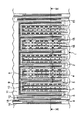
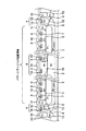
【解決手段】P型シリコン基板1上に縦型PNPトランジスタを複数並べて構成されたパワートランジスタにおいて、前記P型シリコン基板1と前記複数の縦型PNPトランジスタのコレクタを分離するためのN+型埋込層2の電極部aをパワートランジスタの能動領域内に1箇所または複数有する。
【選択図】図1
Description
2…N+型埋込層、
3…P+型コレクタ埋込層、
4…N型エピタキシャル層、
5…N+型ベースウェル層、
6…P+型コレクタ層、
7…P+型エミッタ層、
8…N+型ベース層、
9…共通エミッタメタル配線、
10…共通ベースメタル配線、
11…共通コレクタメタル配線、
12…N+型埋込層のメタル配線、
13…P+型埋込分離層、
15…N+型拡散層、
16…P+型分離層、
18…N+型電極層、
20…酸化膜(絶縁膜)。
Claims (8)
- P型シリコン基板上に縦型PNPトランジスタを複数形成して構成されたパワートランジスタにおいて、
前記P型シリコン基板と前記複数の縦型PNPトランジスタのコレクタを分離するために形成されたN+型埋込層の電極部をパワートランジスタの能動領域内に1箇所または複数設けたことを特徴とするパワートランジスタ。 - 請求項1に記載のパワートランジスタにおいて、
前記電極部の少なくとも一部はパワートランジスタの能動領域上に配線されたパワートランジスタの共通エミッタメタル配線上に設けられたことを特徴とするパワートランジスタ。 - 請求項1に記載のパワートランジスタにおいて、
前記電極部は前記N+型埋込層上に形成され、オーミック接触するためのN+型電極層とN+型拡散層で形成されたことを特徴とするパワートランジスタ。
に記載のパワートランジスタにおいて、 - 請求項3に記載のパワートランジスタにおいて、
前記N+型拡散層は、前記複数の縦型PNPトランジスタのベース領域としてのN+型ベースウェル層と同時に形成されたことを特徴とするパワートランジスタ。 - 請求項3に記載のパワートランジスタにおいて、
前記N+型拡散層は、前記P型シリコン基板上に形成されたN型エピタキシャル層よりも濃い不純物濃度1×10¹⁶〜1×10¹⁷atoms/cm3の範囲で形成されたことを特徴とするパワートランジスタ。 - 請求項3に記載のパワートランジスタにおいて、
前記N+型拡散層は、パワートランジスタ底面にある前記N+型埋込層に到達するまで不純物を拡散して形成されたことを特徴とするパワートランジスタ。 - 請求項1に記載のパワートランジスタにおいて、
前記1または複数の電極部が、隣接する各電極部までの距離が均等になるように配置されていることを特徴とするパワートランジスタ。 - 請求項1乃至7のいずれか1つに記載のパワートランジスタを用いたことを特徴とする半導体集積回路。
Priority Applications (3)
| Application Number | Priority Date | Filing Date | Title |
|---|---|---|---|
| JP2003404517A JP4460272B2 (ja) | 2002-12-11 | 2003-12-03 | パワートランジスタおよびそれを用いた半導体集積回路 |
| US10/735,399 US20050056907A1 (en) | 2002-12-11 | 2003-12-11 | Power transistor and semiconductor integrated circuit using the same |
| CNA2003101225589A CN1507070A (zh) | 2002-12-11 | 2003-12-11 | 功率晶体管及使用它的半导体集成电路 |
Applications Claiming Priority (2)
| Application Number | Priority Date | Filing Date | Title |
|---|---|---|---|
| JP2002359117 | 2002-12-11 | ||
| JP2003404517A JP4460272B2 (ja) | 2002-12-11 | 2003-12-03 | パワートランジスタおよびそれを用いた半導体集積回路 |
Publications (2)
| Publication Number | Publication Date |
|---|---|
| JP2004207702A true JP2004207702A (ja) | 2004-07-22 |
| JP4460272B2 JP4460272B2 (ja) | 2010-05-12 |
Family
ID=32828565
Family Applications (1)
| Application Number | Title | Priority Date | Filing Date |
|---|---|---|---|
| JP2003404517A Expired - Fee Related JP4460272B2 (ja) | 2002-12-11 | 2003-12-03 | パワートランジスタおよびそれを用いた半導体集積回路 |
Country Status (3)
| Country | Link |
|---|---|
| US (1) | US20050056907A1 (ja) |
| JP (1) | JP4460272B2 (ja) |
| CN (1) | CN1507070A (ja) |
Cited By (2)
| Publication number | Priority date | Publication date | Assignee | Title |
|---|---|---|---|---|
| JP2006186159A (ja) * | 2004-12-28 | 2006-07-13 | Renesas Technology Corp | 半導体装置およびそれを用いた無線通信機器 |
| US8232623B2 (en) | 2008-02-18 | 2012-07-31 | Keiji Mita | Semiconductor device |
Families Citing this family (5)
| Publication number | Priority date | Publication date | Assignee | Title |
|---|---|---|---|---|
| US7436043B2 (en) * | 2004-12-21 | 2008-10-14 | Taiwan Semiconductor Manufacturing Co., Ltd | N-well and N+ buried layer isolation by auto doping to reduce chip size |
| JP5048242B2 (ja) * | 2005-11-30 | 2012-10-17 | オンセミコンダクター・トレーディング・リミテッド | 半導体装置及びその製造方法 |
| CN100459145C (zh) * | 2006-12-15 | 2009-02-04 | 东南大学 | 高压功率集成电路隔离结构 |
| CN103730486A (zh) * | 2013-10-18 | 2014-04-16 | 苏州贝克微电子有限公司 | 一种横向pnp功率晶体管 |
| KR102495452B1 (ko) | 2016-06-29 | 2023-02-02 | 삼성전자주식회사 | 반도체 장치 |
Family Cites Families (4)
| Publication number | Priority date | Publication date | Assignee | Title |
|---|---|---|---|---|
| US5121185A (en) * | 1987-10-09 | 1992-06-09 | Hitachi, Ltd. | Monolithic semiconductor IC device including blocks having different functions with different breakdown voltages |
| US5455447A (en) * | 1989-05-10 | 1995-10-03 | Texas Instruments Incorporated | Vertical PNP transistor in merged bipolar/CMOS technology |
| US5179432A (en) * | 1991-08-15 | 1993-01-12 | Micrel, Inc. | Integrated PNP power bipolar transistor with low injection into substrate |
| US5648281A (en) * | 1992-09-21 | 1997-07-15 | Siliconix Incorporated | Method for forming an isolation structure and a bipolar transistor on a semiconductor substrate |
-
2003
- 2003-12-03 JP JP2003404517A patent/JP4460272B2/ja not_active Expired - Fee Related
- 2003-12-11 CN CNA2003101225589A patent/CN1507070A/zh active Pending
- 2003-12-11 US US10/735,399 patent/US20050056907A1/en not_active Abandoned
Cited By (5)
| Publication number | Priority date | Publication date | Assignee | Title |
|---|---|---|---|---|
| JP2006186159A (ja) * | 2004-12-28 | 2006-07-13 | Renesas Technology Corp | 半導体装置およびそれを用いた無線通信機器 |
| US8227836B2 (en) | 2004-12-28 | 2012-07-24 | Murata Manufacturing Co., Ltd. | Semiconductor device and radio communication device |
| US8860093B2 (en) | 2004-12-28 | 2014-10-14 | Murata Manufacturing Co., Ltd. | Semiconductor device and radio communication device |
| US9263559B2 (en) | 2004-12-28 | 2016-02-16 | Murata Manufacturing Co., Ltd. | Semiconductor device and radio communication device |
| US8232623B2 (en) | 2008-02-18 | 2012-07-31 | Keiji Mita | Semiconductor device |
Also Published As
| Publication number | Publication date |
|---|---|
| CN1507070A (zh) | 2004-06-23 |
| US20050056907A1 (en) | 2005-03-17 |
| JP4460272B2 (ja) | 2010-05-12 |
Similar Documents
| Publication | Publication Date | Title |
|---|---|---|
| KR100208632B1 (ko) | 반도체 집적 회로 및 그 제조 방법 | |
| JPH07297373A (ja) | 誘導性負荷要素に対する集積ドライバ回路装置 | |
| JP4460272B2 (ja) | パワートランジスタおよびそれを用いた半導体集積回路 | |
| US7420260B2 (en) | Power semiconductor device for suppressing substrate recirculation current and method of fabricating power semiconductor device | |
| US4160990A (en) | Semiconductor devices and circuit arrangements including such devices | |
| JP2680848B2 (ja) | 半導体記憶装置 | |
| US20040120085A1 (en) | Semiconductor device with surge protection circuit | |
| JPS6359262B2 (ja) | ||
| JP2518929B2 (ja) | バイポ―ラ型半導体集積回路 | |
| JP2518880B2 (ja) | 半導体装置 | |
| JP4231658B2 (ja) | 半導体装置およびその製造方法 | |
| JP2833913B2 (ja) | バイポーラ集積回路装置 | |
| JPH0428148B2 (ja) | ||
| JPS5885558A (ja) | セミカスタム半導体装置 | |
| JPS63244876A (ja) | 相補型mis半導体装置及びその製造方法 | |
| JPH0322693B2 (ja) | ||
| JPH0236538A (ja) | 半導体装置 | |
| JPS6223466B2 (ja) | ||
| JPS6031105B2 (ja) | 半導体装置 | |
| JPS61208260A (ja) | 半導体装置 | |
| JPH09116021A (ja) | 半導体集積回路とその製造方法 | |
| JPH07240469A (ja) | バイポーラロジック | |
| JPH0442828B2 (ja) | ||
| JPS61276340A (ja) | 半導体集積回路装置 | |
| JP2000012713A (ja) | 半導体集積回路装置 |
Legal Events
| Date | Code | Title | Description |
|---|---|---|---|
| A621 | Written request for application examination |
Free format text: JAPANESE INTERMEDIATE CODE: A621 Effective date: 20060125 |
|
| A977 | Report on retrieval |
Free format text: JAPANESE INTERMEDIATE CODE: A971007 Effective date: 20071129 |
|
| A131 | Notification of reasons for refusal |
Free format text: JAPANESE INTERMEDIATE CODE: A131 Effective date: 20091110 |
|
| A521 | Request for written amendment filed |
Free format text: JAPANESE INTERMEDIATE CODE: A523 Effective date: 20091217 |
|
| TRDD | Decision of grant or rejection written | ||
| A01 | Written decision to grant a patent or to grant a registration (utility model) |
Free format text: JAPANESE INTERMEDIATE CODE: A01 Effective date: 20100209 |
|
| A01 | Written decision to grant a patent or to grant a registration (utility model) |
Free format text: JAPANESE INTERMEDIATE CODE: A01 |
|
| A61 | First payment of annual fees (during grant procedure) |
Free format text: JAPANESE INTERMEDIATE CODE: A61 Effective date: 20100212 |
|
| R150 | Certificate of patent or registration of utility model |
Free format text: JAPANESE INTERMEDIATE CODE: R150 |
|
| FPAY | Renewal fee payment (event date is renewal date of database) |
Free format text: PAYMENT UNTIL: 20130219 Year of fee payment: 3 |
|
| FPAY | Renewal fee payment (event date is renewal date of database) |
Free format text: PAYMENT UNTIL: 20130219 Year of fee payment: 3 |
|
| FPAY | Renewal fee payment (event date is renewal date of database) |
Free format text: PAYMENT UNTIL: 20140219 Year of fee payment: 4 |
|
| LAPS | Cancellation because of no payment of annual fees |