JP4267611B2 - マイクロマシニングされたセンサ用懸下部材の製造方法 - Google Patents
マイクロマシニングされたセンサ用懸下部材の製造方法 Download PDFInfo
- Publication number
- JP4267611B2 JP4267611B2 JP2005271996A JP2005271996A JP4267611B2 JP 4267611 B2 JP4267611 B2 JP 4267611B2 JP 2005271996 A JP2005271996 A JP 2005271996A JP 2005271996 A JP2005271996 A JP 2005271996A JP 4267611 B2 JP4267611 B2 JP 4267611B2
- Authority
- JP
- Japan
- Prior art keywords
- wafer
- silicon layer
- mass
- frame member
- layer
- Prior art date
- Legal status (The legal status is an assumption and is not a legal conclusion. Google has not performed a legal analysis and makes no representation as to the accuracy of the status listed.)
- Expired - Lifetime
Links
- 238000000034 method Methods 0.000 title claims description 25
- 238000004519 manufacturing process Methods 0.000 title claims description 24
- 239000000725 suspension Substances 0.000 title claims description 24
- 235000012431 wafers Nutrition 0.000 claims description 77
- XUIMIQQOPSSXEZ-UHFFFAOYSA-N Silicon Chemical compound [Si] XUIMIQQOPSSXEZ-UHFFFAOYSA-N 0.000 claims description 59
- 229910052710 silicon Inorganic materials 0.000 claims description 59
- 239000010703 silicon Substances 0.000 claims description 59
- 238000005530 etching Methods 0.000 claims description 22
- 238000003486 chemical etching Methods 0.000 claims description 8
- 238000001020 plasma etching Methods 0.000 claims description 8
- 238000001312 dry etching Methods 0.000 claims description 6
- 239000002210 silicon-based material Substances 0.000 claims description 5
- 239000000758 substrate Substances 0.000 claims 1
- 229920002120 photoresistant polymer Polymers 0.000 description 17
- VYPSYNLAJGMNEJ-UHFFFAOYSA-N Silicium dioxide Chemical compound O=[Si]=O VYPSYNLAJGMNEJ-UHFFFAOYSA-N 0.000 description 13
- 238000005459 micromachining Methods 0.000 description 13
- KWYUFKZDYYNOTN-UHFFFAOYSA-M Potassium hydroxide Chemical compound [OH-].[K+] KWYUFKZDYYNOTN-UHFFFAOYSA-M 0.000 description 11
- HEMHJVSKTPXQMS-UHFFFAOYSA-M Sodium hydroxide Chemical compound [OH-].[Na+] HEMHJVSKTPXQMS-UHFFFAOYSA-M 0.000 description 6
- 239000000377 silicon dioxide Substances 0.000 description 6
- 235000012239 silicon dioxide Nutrition 0.000 description 6
- 238000001039 wet etching Methods 0.000 description 6
- 238000001514 detection method Methods 0.000 description 5
- 239000000126 substance Substances 0.000 description 5
- 238000004140 cleaning Methods 0.000 description 4
- 239000000463 material Substances 0.000 description 4
- 229910021421 monocrystalline silicon Inorganic materials 0.000 description 4
- 150000004767 nitrides Chemical class 0.000 description 4
- 238000000206 photolithography Methods 0.000 description 4
- ZOXJGFHDIHLPTG-UHFFFAOYSA-N Boron Chemical compound [B] ZOXJGFHDIHLPTG-UHFFFAOYSA-N 0.000 description 3
- 230000001133 acceleration Effects 0.000 description 3
- 229910052796 boron Inorganic materials 0.000 description 3
- 239000013078 crystal Substances 0.000 description 3
- 239000012535 impurity Substances 0.000 description 3
- 125000000896 monocarboxylic acid group Chemical group 0.000 description 3
- 238000012545 processing Methods 0.000 description 3
- 239000004065 semiconductor Substances 0.000 description 3
- XLYOFNOQVPJJNP-UHFFFAOYSA-N water Chemical compound O XLYOFNOQVPJJNP-UHFFFAOYSA-N 0.000 description 3
- OAICVXFJPJFONN-UHFFFAOYSA-N Phosphorus Chemical compound [P] OAICVXFJPJFONN-UHFFFAOYSA-N 0.000 description 2
- QVGXLLKOCUKJST-UHFFFAOYSA-N atomic oxygen Chemical compound [O] QVGXLLKOCUKJST-UHFFFAOYSA-N 0.000 description 2
- 230000015572 biosynthetic process Effects 0.000 description 2
- 230000000295 complement effect Effects 0.000 description 2
- 230000006835 compression Effects 0.000 description 2
- 238000007906 compression Methods 0.000 description 2
- 229910052751 metal Inorganic materials 0.000 description 2
- 239000002184 metal Substances 0.000 description 2
- 238000012986 modification Methods 0.000 description 2
- 230000004048 modification Effects 0.000 description 2
- 229910052760 oxygen Inorganic materials 0.000 description 2
- 239000001301 oxygen Substances 0.000 description 2
- 239000011574 phosphorus Substances 0.000 description 2
- 229910052698 phosphorus Inorganic materials 0.000 description 2
- 238000007493 shaping process Methods 0.000 description 2
- 239000011800 void material Substances 0.000 description 2
- 229910004298 SiO 2 Inorganic materials 0.000 description 1
- 229910000831 Steel Inorganic materials 0.000 description 1
- 239000002253 acid Substances 0.000 description 1
- 230000006978 adaptation Effects 0.000 description 1
- 239000000853 adhesive Substances 0.000 description 1
- 230000001070 adhesive effect Effects 0.000 description 1
- LDDQLRUQCUTJBB-UHFFFAOYSA-N ammonium fluoride Chemical compound [NH4+].[F-] LDDQLRUQCUTJBB-UHFFFAOYSA-N 0.000 description 1
- 238000000347 anisotropic wet etching Methods 0.000 description 1
- 238000005219 brazing Methods 0.000 description 1
- 239000003795 chemical substances by application Substances 0.000 description 1
- 239000011248 coating agent Substances 0.000 description 1
- 238000000576 coating method Methods 0.000 description 1
- 239000008367 deionised water Substances 0.000 description 1
- 229910021641 deionized water Inorganic materials 0.000 description 1
- 238000000151 deposition Methods 0.000 description 1
- 230000008021 deposition Effects 0.000 description 1
- 238000001035 drying Methods 0.000 description 1
- 238000005516 engineering process Methods 0.000 description 1
- 239000007789 gas Substances 0.000 description 1
- 229910052737 gold Inorganic materials 0.000 description 1
- 238000010438 heat treatment Methods 0.000 description 1
- JEIPFZHSYJVQDO-UHFFFAOYSA-N iron(III) oxide Inorganic materials O=[Fe]O[Fe]=O JEIPFZHSYJVQDO-UHFFFAOYSA-N 0.000 description 1
- 238000004518 low pressure chemical vapour deposition Methods 0.000 description 1
- 238000005259 measurement Methods 0.000 description 1
- 150000002739 metals Chemical class 0.000 description 1
- 239000000203 mixture Substances 0.000 description 1
- 229920000620 organic polymer Polymers 0.000 description 1
- 230000003647 oxidation Effects 0.000 description 1
- 238000007254 oxidation reaction Methods 0.000 description 1
- 238000000059 patterning Methods 0.000 description 1
- 229910021426 porous silicon Inorganic materials 0.000 description 1
- 229910052814 silicon oxide Inorganic materials 0.000 description 1
- 238000005476 soldering Methods 0.000 description 1
- 239000010959 steel Substances 0.000 description 1
- 238000012546 transfer Methods 0.000 description 1
Images


Classifications
-
- G—PHYSICS
- G01—MEASURING; TESTING
- G01P—MEASURING LINEAR OR ANGULAR SPEED, ACCELERATION, DECELERATION, OR SHOCK; INDICATING PRESENCE, ABSENCE, OR DIRECTION, OF MOVEMENT
- G01P15/00—Measuring acceleration; Measuring deceleration; Measuring shock, i.e. sudden change of acceleration
- G01P15/02—Measuring acceleration; Measuring deceleration; Measuring shock, i.e. sudden change of acceleration by making use of inertia forces using solid seismic masses
- G01P15/08—Measuring acceleration; Measuring deceleration; Measuring shock, i.e. sudden change of acceleration by making use of inertia forces using solid seismic masses with conversion into electric or magnetic values
- G01P15/0802—Details
-
- Y—GENERAL TAGGING OF NEW TECHNOLOGICAL DEVELOPMENTS; GENERAL TAGGING OF CROSS-SECTIONAL TECHNOLOGIES SPANNING OVER SEVERAL SECTIONS OF THE IPC; TECHNICAL SUBJECTS COVERED BY FORMER USPC CROSS-REFERENCE ART COLLECTIONS [XRACs] AND DIGESTS
- Y10—TECHNICAL SUBJECTS COVERED BY FORMER USPC
- Y10S—TECHNICAL SUBJECTS COVERED BY FORMER USPC CROSS-REFERENCE ART COLLECTIONS [XRACs] AND DIGESTS
- Y10S148/00—Metal treatment
- Y10S148/012—Bonding, e.g. electrostatic for strain gauges
Landscapes
- Physics & Mathematics (AREA)
- General Physics & Mathematics (AREA)
- Micromachines (AREA)
- Pressure Sensors (AREA)
- Drying Of Semiconductors (AREA)
- Weting (AREA)
- Testing Or Calibration Of Command Recording Devices (AREA)
Description
(1)ストレスを除去するためのばねの整形;
(2)直線性を最大とするためのばねの整形;
(3)プリローディング条件を形成するためのばねの被覆;および
(4)プリロード条件を形成するためのばねのドーピング。
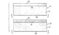
HNO3:HF)を、特に図4に示すように中心質量部と外側支持フレームの間のばねを形成する領域の露出したP++層16に対し、制御された短い時間だけ加える。P++層とその上のEPI層の除去量が結果としてのばねの厚さを制御する。薄い酸化物層25(図3)を適当なエッチング剤(好適には6:1BOE)で除去する。
段階
1 両面を研磨した厚さ500ミクロンの4.1インチシリコンウエハを
用意する。
2 EPI層を厚さ500ミクロンまで成長させる。
3 0.3ミクロンの層をつくるようにドライ、ウェットおよびドライの
条件を交互に用いてウエハを熱酸化する。
4 ウエハをそのEPI側を下にして回転させる。EPI側をホットプレ
ートで強く焼く。
5 ウエハをその背面側を下にして回転させる。ホットプレートで背面を
弱く焼く。(横方向ベント穴が望ましくない場合には段階12に移る)
6 横ベントマスクを用いて背面側をパターン化する。
7 6:1BOEを与える。次にホトレジストを背面から除去しそして
RCA洗浄を行う。
8 3ミクロンの層をつくるためにドライ、ウェットおよびドライの条件
を交互に用いてウエハを熱酸化する。
9 LPCVDニトライドにより0.15ミクロンの厚さの窒化物をつく
る。
10 ウエハをそのEPI側を下にして回転し、ホットプレート上でそれを
強く焼く。
11 ウエハをその背面側を下にして回転し、それを弱く焼く。
12 ODEキャビティマスクを用いてウエハの背面側をホトレジストでパ
ターン化する。
13 プラズマエッチング;窒化物のエッチング380Torr、175ワ
ット、SF6
14 ウェットエッチング;6:1BOE;ホトレジスト除去。
15 ウェットエッチング;深さ450ミクロンまでのKOHエッチング
(33重量%):消イオン化水(DI H2O)による洗浄。
16 ウェットエッチング:P++エッチストップまでのC5OH(60%)
によるエッチング;DI H2O洗浄。
17 整合孔のみにドロッパを用いたP++(8:3:1、CH3COOH:
HNO3:HF)の選択エッチング(整合孔は図示せず;整合孔は
質量部の溶着のためにウエハを整合させるために用いられる)
18 ウェットエッチング:整合孔で光が明確となるまでのKOH(33
重量%)エッチング。DI H2O洗浄。
19 P++層ウエハ全体のウェットエッチング;
(8:3:1、CH3COOH:HNO3:HF)。
20 97:3 HNO3:HFを用いて茶色のさび(多孔性シリコン)
を除去する;DI H2O洗浄。
21 裏側の燐と共に窒化物をはぎとる;6:1BOEで酸化物をはぎとる。
22 RCA洗浄。
23 2個のウエハの質量部分を溶着;整合。
24 ウェットO2で酸化してベント穴を閉じる。
25 ウェットエッチング:酸化物をBOEで除去、DIH2O洗浄、
スピン乾燥。
26 両側を100ÅのCrおよび1000ÅのAuで金属化。
27 両側についてスピン;次に弱く焼く。
28 ばね形状を表わす金属ワッシャを用いたホトレジストで両側を
パターン化する。
29 Auのエッチング、Crのエッチング。
30 両側についてスピンし、弱く焼く。
31 ばねマスクおよび電気接点マスクを用いたホトレジストで前側を
パターン化する;強く焼く。
32 プラズマエッチング:両側のシリコンプラズマエッチング
(380Torr、175ワット)。
33 プラズマエッチング:両側のO2プラズマストリップ
(400mTorr)。
Claims (6)
- 側壁を有するフレーム部材と、上記フレーム部材の上記側壁から隔離されて上記側壁内に置かれた質量部材と、上記フレーム部材と上記質量部材と接続する複数の懸下部材とを備えたセンサを製造する方法であって、
(a)第1シリコンウエハ(10)を処理して、エッチストップ層(16)によって分離される、バルクシリコン層(14)およびエピタキシャル成長シリコン層(18)を有する処理されたウエハを製造する段階と、
(b)上記フレーム部材(23)の側壁と上記質量部材との間のスペース(22)を規定するパターンに一致した深さを形成するために、上記処理されたウエハのバルクシリコン層側から、上記エッチストップ層(16)に達するまで上記バルクシリコン層を化学的エッチングする段階と、
(c)上記スペースに隣接したエピタキシャル成長シリコン層を提供するために、上記フレーム部材(23)の側壁と上記質量部材との間のスペース(22)から上記スペース内の上記エッチストップ層(16)のみを除去する段階と、
(d)上記スペース内のエピタキシャル成長シリコン材料を除去しこれにより上記フレーム部材(23)から上記質量部材(21)を懸下する懸下部材を形成するために、懸下部材パターンに従って、上記処理されたウエハの上記エピタキシャル成長シリコン層からドライエッチングする段階と、
を備え、
上記(a)、(b)、(c)の段階は第2シリコンウエハ(12)に対して繰り返され、
上記質量部材と上記フレーム部材(23)を規定するために上記第1および第2シリコンウエハを接合し、上記エピタキシャル成長シリコン層が結合されたウエハの外表面となるようにする段階と、
懸下部材パターンに従って、上記第1および第2シリコンウエハのそれぞれの上記エピタキシャル成長シリコン層(18)側からドライエッチングし、上記スペース内のエピタキシャル成長シリコン層(18)を除去し、これにより上記フレーム部材(23)から上記質量部材(21)を懸下する懸下部材を形成する段階と、
を備えたことを特徴とするセンサを製造する方法。 - 上記ドライエッチングする段階は、長方形状の質量部材の角を回るL字型の上記懸下部材を形成するためにプラズマエッチングする段階を含むことを特徴とする請求項1記載のセンサを製造する方法。
- 上記化学的エッチングする段階は、上記エッチストップ層(16)を除去するばかりでなく上記フレーム部材の上記側壁と上記懸下された質量部材の間の上記スペースに隣接する上記エピタキシャル成長シリコン層(18)の一部分を除去するための制御された時間実行され、残置する上記エピタキシャル成長シリコン層の厚さを制御することを特徴とする請求項1または2記載のセンサを製造する方法。
- 上記エッチストップ層(16)を除去する段階は、(b)の段階の後に、上記ウエハの上記バルクシリコン層(14)側から化学的エッチングを行って上記スペース(22)内の上記エッチストップ層(16)のみを除去し、これによりエピタキシャル成長シリコン材料のみからなる上記懸下部材を形成する段階を含むことを特徴とする請求項1乃至3のいずれかに記載のセンサを製造する方法。
- 上記質量部材は、上記フレーム部材(23)の対応する側壁から離間された4つの質量部材側壁を有し、各懸下部材は2本の交差する脚を有し、1つの脚はフレーム部材側壁への接続部に対して90度の角度で取り付けられ、他の脚は上記フレーム部材側壁に対して直角に配置された質量部材側壁への接続部に対して90度の角度で取り付けられていることを特徴とする請求項1乃至4のいずれかに記載のセンサを製造する方法。
- 側壁を有するフレーム部材と、上記フレーム部材の上記側壁から隔離されて上記側壁内に置かれた質量部材と、上記フレーム部材と上記質量部材と接続する複数の懸下部材とを備えたセンサを製造する方法であって、
(a)第1シリコンウエハ(10)を処理して、エッチストップ層(16)によって分離される、バルクシリコン層(14)およびエピタキシャル成長シリコン層(18)を有する処理されたウエハを製造する段階と、
(b)上記処理されたウエハのバルクシリコン層側から、上記エッチストップ層(16)に達するまで上記バルクシリコン層を化学的なエッチングを行い、上記フレーム部材(23)の側壁と上記質量部材との間のスペース(22)を規定するパターンに一致した深さを形成する段階と、
(c)前記処理されたウエハの上記バルクシリコン層側から化学的エッチングを行い、前記(b)の段階で露出した上記エッチストップ層を除去する段階と、
(d)第2シリコンウエハ(12)に対して前記(a)、(b)および(c)の段階を繰り返す段階と、それから
(e)前記第1および第2ウエハを互いに接着して前記エピタキシャル成長シリコン層(18)が接着されたウエハ(14)の外側表面にあるように前記質量部材および前記フレーム部材を規定する段階と、
(f)前記スペース内の前記エピタキシャル成長シリコン層(18)を除去することにより、前記フレーム部材(23)から前記質量部材を懸下する懸下部材を残すように、前記ウエハの前記エピタキシャル成長シリコン層側から懸下部材パターンに従ってドライエッチングを行う段階と、
を備えたことを特徴とするセンサを製造する方法。
Applications Claiming Priority (1)
| Application Number | Priority Date | Filing Date | Title |
|---|---|---|---|
| US08/218,363 US5484073A (en) | 1994-03-28 | 1994-03-28 | Method for fabricating suspension members for micromachined sensors |
Related Parent Applications (1)
| Application Number | Title | Priority Date | Filing Date |
|---|---|---|---|
| JP52519695A Division JP3741723B2 (ja) | 1994-03-28 | 1995-03-16 | マイクロマシニングされたセンサ用懸下部材の製造方法 |
Publications (2)
| Publication Number | Publication Date |
|---|---|
| JP2006116693A JP2006116693A (ja) | 2006-05-11 |
| JP4267611B2 true JP4267611B2 (ja) | 2009-05-27 |
Family
ID=22814808
Family Applications (2)
| Application Number | Title | Priority Date | Filing Date |
|---|---|---|---|
| JP52519695A Expired - Fee Related JP3741723B2 (ja) | 1994-03-28 | 1995-03-16 | マイクロマシニングされたセンサ用懸下部材の製造方法 |
| JP2005271996A Expired - Lifetime JP4267611B2 (ja) | 1994-03-28 | 2005-09-20 | マイクロマシニングされたセンサ用懸下部材の製造方法 |
Family Applications Before (1)
| Application Number | Title | Priority Date | Filing Date |
|---|---|---|---|
| JP52519695A Expired - Fee Related JP3741723B2 (ja) | 1994-03-28 | 1995-03-16 | マイクロマシニングされたセンサ用懸下部材の製造方法 |
Country Status (7)
| Country | Link |
|---|---|
| US (1) | US5484073A (ja) |
| EP (1) | EP0700580B1 (ja) |
| JP (2) | JP3741723B2 (ja) |
| AU (1) | AU2102195A (ja) |
| CA (1) | CA2159642C (ja) |
| DE (1) | DE69531580T2 (ja) |
| WO (1) | WO1995026567A1 (ja) |
Families Citing this family (50)
| Publication number | Priority date | Publication date | Assignee | Title |
|---|---|---|---|---|
| US5777226A (en) * | 1994-03-28 | 1998-07-07 | I/O Sensors, Inc. | Sensor structure with L-shaped spring legs |
| JPH0936385A (ja) * | 1995-07-25 | 1997-02-07 | Nissan Motor Co Ltd | 半導体装置の製造方法 |
| DE19539049A1 (de) * | 1995-10-20 | 1997-04-24 | Bosch Gmbh Robert | Verfahren zur Herstellung eines Coriolis-Drehratensensors |
| DE19603829A1 (de) * | 1996-02-02 | 1997-08-07 | Daimler Benz Ag | Verfahren zur Herstellung von mikromechanischen Strukturen aus Silizium |
| US5971527A (en) * | 1996-10-29 | 1999-10-26 | Xerox Corporation | Ink jet channel wafer for a thermal ink jet printhead |
| FR2763745B1 (fr) * | 1997-05-23 | 1999-08-27 | Sextant Avionique | Procede de fabrication d'un micro-capteur en silicium usine |
| US6379989B1 (en) * | 1998-12-23 | 2002-04-30 | Xerox Corporation | Process for manufacture of microoptomechanical structures |
| EP1169657A4 (en) * | 1999-03-17 | 2003-03-05 | Input Output Inc | PROBE CALIBRATION |
| US6871544B1 (en) | 1999-03-17 | 2005-03-29 | Input/Output, Inc. | Sensor design and process |
| EP1096260B1 (en) * | 1999-10-29 | 2005-06-15 | SensoNor asa | Micromechanical device |
| EP2136215A3 (en) | 2000-06-21 | 2014-01-01 | ION Geophysical Corporation | Accelerometer with folded beams |
| GB2371119A (en) * | 2000-09-25 | 2002-07-17 | Marconi Caswell Ltd | Micro electro-mechanical systems |
| US6479315B1 (en) | 2000-11-27 | 2002-11-12 | Microscan Systems, Inc. | Process for manufacturing micromechanical and microoptomechanical structures with single crystal silicon exposure step |
| US6479311B1 (en) | 2000-11-27 | 2002-11-12 | Microscan Systems, Inc. | Process for manufacturing micromechanical and microoptomechanical structures with pre-applied patterning |
| US6506620B1 (en) | 2000-11-27 | 2003-01-14 | Microscan Systems Incorporated | Process for manufacturing micromechanical and microoptomechanical structures with backside metalization |
| FI113704B (fi) * | 2001-03-21 | 2004-05-31 | Vti Technologies Oy | Menetelmä piianturin valmistamiseksi sekä piianturi |
| DE60232250D1 (de) * | 2001-08-20 | 2009-06-18 | Honeywell Int Inc | Bogenförmige federelemente für mikro-elektromechanischen beschleunigungssensor |
| US20040240034A1 (en) * | 2001-11-30 | 2004-12-02 | Scharf Bruce R. | Diffraction compensation using a patterned reflector |
| US7140250B2 (en) * | 2005-02-18 | 2006-11-28 | Honeywell International Inc. | MEMS teeter-totter accelerometer having reduced non-linearty |
| US7687126B2 (en) | 2005-08-22 | 2010-03-30 | 3M Innovative Properties Company | Adhesive articles and release liners |
| EP1921042A1 (fr) * | 2006-11-10 | 2008-05-14 | ETA SA Manufacture Horlogère Suisse | Procédé de fabrication de pièces de micromécanique multiniveaux en silicium et pièces ainsi obtenues |
| US9294011B2 (en) * | 2011-02-07 | 2016-03-22 | Ion Geophysical Corporation | Method and apparatus for sensing underwater signals |
| US8519515B2 (en) | 2011-04-13 | 2013-08-27 | United Microlectronics Corp. | TSV structure and method for forming the same |
| US8481425B2 (en) | 2011-05-16 | 2013-07-09 | United Microelectronics Corp. | Method for fabricating through-silicon via structure |
| US8822336B2 (en) | 2011-06-16 | 2014-09-02 | United Microelectronics Corp. | Through-silicon via forming method |
| US8828745B2 (en) | 2011-07-06 | 2014-09-09 | United Microelectronics Corp. | Method for manufacturing through-silicon via |
| US8518823B2 (en) | 2011-12-23 | 2013-08-27 | United Microelectronics Corp. | Through silicon via and method of forming the same |
| US8609529B2 (en) | 2012-02-01 | 2013-12-17 | United Microelectronics Corp. | Fabrication method and structure of through silicon via |
| US8691600B2 (en) | 2012-05-02 | 2014-04-08 | United Microelectronics Corp. | Method for testing through-silicon-via (TSV) structures |
| US8691688B2 (en) | 2012-06-18 | 2014-04-08 | United Microelectronics Corp. | Method of manufacturing semiconductor structure |
| US9275933B2 (en) | 2012-06-19 | 2016-03-01 | United Microelectronics Corp. | Semiconductor device |
| US8900996B2 (en) | 2012-06-21 | 2014-12-02 | United Microelectronics Corp. | Through silicon via structure and method of fabricating the same |
| US8525296B1 (en) | 2012-06-26 | 2013-09-03 | United Microelectronics Corp. | Capacitor structure and method of forming the same |
| US8912844B2 (en) | 2012-10-09 | 2014-12-16 | United Microelectronics Corp. | Semiconductor structure and method for reducing noise therein |
| DE102012219660B4 (de) * | 2012-10-26 | 2023-10-12 | Robert Bosch Gmbh | Mechanisches Bauteil |
| US9035457B2 (en) | 2012-11-29 | 2015-05-19 | United Microelectronics Corp. | Substrate with integrated passive devices and method of manufacturing the same |
| US8716104B1 (en) | 2012-12-20 | 2014-05-06 | United Microelectronics Corp. | Method of fabricating isolation structure |
| CN104045049A (zh) * | 2013-03-12 | 2014-09-17 | 北京大学 | 一种基于硅层转移技术(solt)的高精度加速度计的加工方法 |
| US8884398B2 (en) | 2013-04-01 | 2014-11-11 | United Microelectronics Corp. | Anti-fuse structure and programming method thereof |
| US9287173B2 (en) | 2013-05-23 | 2016-03-15 | United Microelectronics Corp. | Through silicon via and process thereof |
| US9123730B2 (en) | 2013-07-11 | 2015-09-01 | United Microelectronics Corp. | Semiconductor device having through silicon trench shielding structure surrounding RF circuit |
| US9024416B2 (en) | 2013-08-12 | 2015-05-05 | United Microelectronics Corp. | Semiconductor structure |
| US8916471B1 (en) | 2013-08-26 | 2014-12-23 | United Microelectronics Corp. | Method for forming semiconductor structure having through silicon via for signal and shielding structure |
| US9048223B2 (en) | 2013-09-03 | 2015-06-02 | United Microelectronics Corp. | Package structure having silicon through vias connected to ground potential |
| US9117804B2 (en) | 2013-09-13 | 2015-08-25 | United Microelectronics Corporation | Interposer structure and manufacturing method thereof |
| US9343359B2 (en) | 2013-12-25 | 2016-05-17 | United Microelectronics Corp. | Integrated structure and method for fabricating the same |
| US10340203B2 (en) | 2014-02-07 | 2019-07-02 | United Microelectronics Corp. | Semiconductor structure with through silicon via and method for fabricating and testing the same |
| US9755139B2 (en) * | 2014-06-30 | 2017-09-05 | Texas Instruments Incorporated | Piezoeletric wet etch process with reduced resist lifting and controlled undercut |
| CN105445495B (zh) * | 2014-07-16 | 2018-11-02 | 中国科学院地质与地球物理研究所 | 一种对称的mems加速度敏感芯片及其制造工艺 |
| US10611628B2 (en) * | 2016-12-29 | 2020-04-07 | Epack, Inc. | MEMS isolation platform with three-dimensional vibration and stress isolation |
Family Cites Families (20)
| Publication number | Priority date | Publication date | Assignee | Title |
|---|---|---|---|---|
| US4021766A (en) * | 1975-07-28 | 1977-05-03 | Aine Harry E | Solid state pressure transducer of the leaf spring type and batch method of making same |
| US4071838A (en) * | 1976-02-09 | 1978-01-31 | Diax Corporation | Solid state force transducer and method of making same |
| US4106976A (en) * | 1976-03-08 | 1978-08-15 | International Business Machines Corporation | Ink jet nozzle method of manufacture |
| US4144516A (en) * | 1976-03-29 | 1979-03-13 | Aine Harry E | Solid state transducer and method of making same |
| US4597003A (en) * | 1983-12-01 | 1986-06-24 | Harry E. Aine | Chemical etching of a semiconductive wafer by undercutting an etch stopped layer |
| JPS6197572A (ja) * | 1984-10-19 | 1986-05-16 | Nissan Motor Co Ltd | 半導体加速度センサの製造方法 |
| US4732647A (en) * | 1984-10-24 | 1988-03-22 | Aine Harry E | Batch method of making miniature capacitive force transducers assembled in wafer form |
| US5000817A (en) * | 1984-10-24 | 1991-03-19 | Aine Harry E | Batch method of making miniature structures assembled in wafer form |
| US4679434A (en) * | 1985-07-25 | 1987-07-14 | Litton Systems, Inc. | Integrated force balanced accelerometer |
| US4670092A (en) * | 1986-04-18 | 1987-06-02 | Rockwell International Corporation | Method of fabricating a cantilever beam for a monolithic accelerometer |
| US4922756A (en) * | 1988-06-20 | 1990-05-08 | Triton Technologies, Inc. | Micro-machined accelerometer |
| JPS6376483A (ja) * | 1986-09-19 | 1988-04-06 | Fujitsu Ltd | 半導体加速度センサの製造方法 |
| US4805456A (en) * | 1987-05-19 | 1989-02-21 | Massachusetts Institute Of Technology | Resonant accelerometer |
| US5195371A (en) * | 1988-01-13 | 1993-03-23 | The Charles Stark Draper Laboratory, Inc. | Semiconductor chip transducer |
| JPH01301181A (ja) * | 1988-05-30 | 1989-12-05 | Mitsubishi Electric Corp | 半導体加速度センサの製造方法 |
| JPH02218172A (ja) * | 1989-02-18 | 1990-08-30 | Nippondenso Co Ltd | 半導体加速度センサの製造方法 |
| US5006487A (en) * | 1989-07-27 | 1991-04-09 | Honeywell Inc. | Method of making an electrostatic silicon accelerometer |
| US5233213A (en) * | 1990-07-14 | 1993-08-03 | Robert Bosch Gmbh | Silicon-mass angular acceleration sensor |
| JP2586359B2 (ja) * | 1990-12-17 | 1997-02-26 | 日本電気株式会社 | 半導体加速度センサおよびその製造方法 |
| JPH05142247A (ja) * | 1991-11-20 | 1993-06-08 | Hitachi Ltd | 半導体加速度センサ |
-
1994
- 1994-03-28 US US08/218,363 patent/US5484073A/en not_active Expired - Lifetime
-
1995
- 1995-03-16 CA CA002159642A patent/CA2159642C/en not_active Expired - Lifetime
- 1995-03-16 WO PCT/US1995/003377 patent/WO1995026567A1/en not_active Ceased
- 1995-03-16 AU AU21021/95A patent/AU2102195A/en not_active Abandoned
- 1995-03-16 EP EP95913752A patent/EP0700580B1/en not_active Expired - Lifetime
- 1995-03-16 DE DE69531580T patent/DE69531580T2/de not_active Expired - Lifetime
- 1995-03-16 JP JP52519695A patent/JP3741723B2/ja not_active Expired - Fee Related
-
2005
- 2005-09-20 JP JP2005271996A patent/JP4267611B2/ja not_active Expired - Lifetime
Also Published As
| Publication number | Publication date |
|---|---|
| WO1995026567A1 (en) | 1995-10-05 |
| EP0700580A4 (en) | 1998-02-11 |
| EP0700580A1 (en) | 1996-03-13 |
| DE69531580D1 (de) | 2003-10-02 |
| DE69531580T2 (de) | 2004-07-01 |
| JPH08511379A (ja) | 1996-11-26 |
| CA2159642A1 (en) | 1995-09-29 |
| US5484073A (en) | 1996-01-16 |
| JP2006116693A (ja) | 2006-05-11 |
| AU2102195A (en) | 1995-10-17 |
| HK1004876A1 (en) | 1998-12-11 |
| CA2159642C (en) | 1999-08-17 |
| EP0700580B1 (en) | 2003-08-27 |
| JP3741723B2 (ja) | 2006-02-01 |
Similar Documents
| Publication | Publication Date | Title |
|---|---|---|
| JP4267611B2 (ja) | マイクロマシニングされたセンサ用懸下部材の製造方法 | |
| US20230224657A1 (en) | Semiconductor devices having a membrane layer with smooth stress-relieving corrugations and methods of fabrication thereof | |
| US6428713B1 (en) | MEMS sensor structure and microfabrication process therefor | |
| CN101820570B (zh) | 麦克风 | |
| US8065919B2 (en) | MEMS device and method for fabricating the same | |
| EP0322093B1 (en) | Rectilinearly deflectable element fabricated from a single wafer | |
| US7563720B2 (en) | Boron doped shell for MEMS device | |
| JPH1022184A (ja) | 基板張り合わせ装置 | |
| JP2002095093A (ja) | コンデンサマイクロホンおよびその製造方法および音声入力装置 | |
| CN210559358U (zh) | 压力传感器 | |
| HK1004876B (en) | Method for fabricating suspension members for micromachined sensors | |
| RU2672033C1 (ru) | Способ формирования областей кремния в объеме кремниевой пластины | |
| CN119349500A (zh) | 一种绝压式传感器的制作方法及绝压式传感器结构 | |
| KR100465914B1 (ko) | 미소 구동기 제조방법 | |
| JPH10144934A (ja) | 半導体圧力センサ及びその製造方法 | |
| Zhang | Dome-Shaped Diaphragm Microtransducers | |
| JP2005337877A (ja) | バーチカルコム及びこれを含むジャイロセンサの製造方法 | |
| JPH0645298A (ja) | 半導体装置の製造方法 | |
| JPH04171930A (ja) | ドライエッチング加工処理方法 |
Legal Events
| Date | Code | Title | Description |
|---|---|---|---|
| A131 | Notification of reasons for refusal |
Free format text: JAPANESE INTERMEDIATE CODE: A131 Effective date: 20080115 |
|
| A601 | Written request for extension of time |
Free format text: JAPANESE INTERMEDIATE CODE: A601 Effective date: 20080415 |
|
| A602 | Written permission of extension of time |
Free format text: JAPANESE INTERMEDIATE CODE: A602 Effective date: 20080418 |
|
| A601 | Written request for extension of time |
Free format text: JAPANESE INTERMEDIATE CODE: A601 Effective date: 20080514 |
|
| A602 | Written permission of extension of time |
Free format text: JAPANESE INTERMEDIATE CODE: A602 Effective date: 20080519 |
|
| A521 | Request for written amendment filed |
Free format text: JAPANESE INTERMEDIATE CODE: A523 Effective date: 20080526 |
|
| A02 | Decision of refusal |
Free format text: JAPANESE INTERMEDIATE CODE: A02 Effective date: 20080620 |
|
| A521 | Request for written amendment filed |
Free format text: JAPANESE INTERMEDIATE CODE: A523 Effective date: 20080917 |
|
| A711 | Notification of change in applicant |
Free format text: JAPANESE INTERMEDIATE CODE: A712 Effective date: 20081121 |
|
| A521 | Request for written amendment filed |
Free format text: JAPANESE INTERMEDIATE CODE: A821 Effective date: 20081121 |
|
| A911 | Transfer to examiner for re-examination before appeal (zenchi) |
Free format text: JAPANESE INTERMEDIATE CODE: A911 Effective date: 20081225 |
|
| TRDD | Decision of grant or rejection written | ||
| A01 | Written decision to grant a patent or to grant a registration (utility model) |
Free format text: JAPANESE INTERMEDIATE CODE: A01 Effective date: 20090123 |
|
| A01 | Written decision to grant a patent or to grant a registration (utility model) |
Free format text: JAPANESE INTERMEDIATE CODE: A01 |
|
| A61 | First payment of annual fees (during grant procedure) |
Free format text: JAPANESE INTERMEDIATE CODE: A61 Effective date: 20090218 |
|
| R150 | Certificate of patent or registration of utility model |
Free format text: JAPANESE INTERMEDIATE CODE: R150 |
|
| FPAY | Renewal fee payment (event date is renewal date of database) |
Free format text: PAYMENT UNTIL: 20120227 Year of fee payment: 3 |
|
| FPAY | Renewal fee payment (event date is renewal date of database) |
Free format text: PAYMENT UNTIL: 20130227 Year of fee payment: 4 |
|
| FPAY | Renewal fee payment (event date is renewal date of database) |
Free format text: PAYMENT UNTIL: 20130227 Year of fee payment: 4 |
|
| FPAY | Renewal fee payment (event date is renewal date of database) |
Free format text: PAYMENT UNTIL: 20140227 Year of fee payment: 5 |
|
| R250 | Receipt of annual fees |
Free format text: JAPANESE INTERMEDIATE CODE: R250 |
|
| R250 | Receipt of annual fees |
Free format text: JAPANESE INTERMEDIATE CODE: R250 |
|
| EXPY | Cancellation because of completion of term |