JP6231625B2 - 基板のボンディング装置及び方法 - Google Patents
基板のボンディング装置及び方法 Download PDFInfo
- Publication number
- JP6231625B2 JP6231625B2 JP2016144567A JP2016144567A JP6231625B2 JP 6231625 B2 JP6231625 B2 JP 6231625B2 JP 2016144567 A JP2016144567 A JP 2016144567A JP 2016144567 A JP2016144567 A JP 2016144567A JP 6231625 B2 JP6231625 B2 JP 6231625B2
- Authority
- JP
- Japan
- Prior art keywords
- substrate
- mounting
- bonding
- mounting surface
- contour
- Prior art date
- Legal status (The legal status is an assumption and is not a legal conclusion. Google has not performed a legal analysis and makes no representation as to the accuracy of the status listed.)
- Active
Links
Images






Classifications
-
- H—ELECTRICITY
- H10—SEMICONDUCTOR DEVICES; ELECTRIC SOLID-STATE DEVICES NOT OTHERWISE PROVIDED FOR
- H10P—GENERIC PROCESSES OR APPARATUS FOR THE MANUFACTURE OR TREATMENT OF DEVICES COVERED BY CLASS H10
- H10P72/00—Handling or holding of wafers, substrates or devices during manufacture or treatment thereof
- H10P72/10—Handling or holding of wafers, substrates or devices during manufacture or treatment thereof using carriers specially adapted therefor, e.g. front opening unified pods [FOUP]
-
- H—ELECTRICITY
- H10—SEMICONDUCTOR DEVICES; ELECTRIC SOLID-STATE DEVICES NOT OTHERWISE PROVIDED FOR
- H10P—GENERIC PROCESSES OR APPARATUS FOR THE MANUFACTURE OR TREATMENT OF DEVICES COVERED BY CLASS H10
- H10P10/00—Bonding of wafers, substrates or parts of devices
- H10P10/12—Bonding of semiconductor wafers or semiconductor substrates to semiconductor wafers or semiconductor substrates
-
- H—ELECTRICITY
- H10—SEMICONDUCTOR DEVICES; ELECTRIC SOLID-STATE DEVICES NOT OTHERWISE PROVIDED FOR
- H10P—GENERIC PROCESSES OR APPARATUS FOR THE MANUFACTURE OR TREATMENT OF DEVICES COVERED BY CLASS H10
- H10P72/00—Handling or holding of wafers, substrates or devices during manufacture or treatment thereof
- H10P72/04—Apparatus for manufacture or treatment
- H10P72/0428—Apparatus for mechanical treatment or grinding or cutting
-
- H—ELECTRICITY
- H10—SEMICONDUCTOR DEVICES; ELECTRIC SOLID-STATE DEVICES NOT OTHERWISE PROVIDED FOR
- H10P—GENERIC PROCESSES OR APPARATUS FOR THE MANUFACTURE OR TREATMENT OF DEVICES COVERED BY CLASS H10
- H10P72/00—Handling or holding of wafers, substrates or devices during manufacture or treatment thereof
- H10P72/70—Handling or holding of wafers, substrates or devices during manufacture or treatment thereof for supporting or gripping
- H10P72/76—Handling or holding of wafers, substrates or devices during manufacture or treatment thereof for supporting or gripping using mechanical means, e.g. clamps or pinches
- H10P72/7604—Handling or holding of wafers, substrates or devices during manufacture or treatment thereof for supporting or gripping using mechanical means, e.g. clamps or pinches the wafers being placed on a susceptor, stage or support
- H10P72/7606—Handling or holding of wafers, substrates or devices during manufacture or treatment thereof for supporting or gripping using mechanical means, e.g. clamps or pinches the wafers being placed on a susceptor, stage or support characterised by edge clamping, e.g. clamping ring
-
- H—ELECTRICITY
- H10—SEMICONDUCTOR DEVICES; ELECTRIC SOLID-STATE DEVICES NOT OTHERWISE PROVIDED FOR
- H10P—GENERIC PROCESSES OR APPARATUS FOR THE MANUFACTURE OR TREATMENT OF DEVICES COVERED BY CLASS H10
- H10P72/00—Handling or holding of wafers, substrates or devices during manufacture or treatment thereof
- H10P72/70—Handling or holding of wafers, substrates or devices during manufacture or treatment thereof for supporting or gripping
- H10P72/78—Handling or holding of wafers, substrates or devices during manufacture or treatment thereof for supporting or gripping using vacuum or suction, e.g. Bernoulli chucks
-
- Y—GENERAL TAGGING OF NEW TECHNOLOGICAL DEVELOPMENTS; GENERAL TAGGING OF CROSS-SECTIONAL TECHNOLOGIES SPANNING OVER SEVERAL SECTIONS OF THE IPC; TECHNICAL SUBJECTS COVERED BY FORMER USPC CROSS-REFERENCE ART COLLECTIONS [XRACs] AND DIGESTS
- Y10—TECHNICAL SUBJECTS COVERED BY FORMER USPC
- Y10T—TECHNICAL SUBJECTS COVERED BY FORMER US CLASSIFICATION
- Y10T156/00—Adhesive bonding and miscellaneous chemical manufacture
- Y10T156/10—Methods of surface bonding and/or assembly therefor
Landscapes
- Container, Conveyance, Adherence, Positioning, Of Wafer (AREA)
- Combinations Of Printed Boards (AREA)
Description
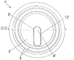
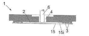
1k 取付け体
2 凹部
2b 底部
3 負圧通路
4,4′ 開口
5,5′ 突出部
6 ピン
7,7′,7″,7′″,7IV 取付け面
8,8′,8″,8′″,8IV 取付け輪郭
9 段部
10 外側の環状部分
11 内側の環状部分
12,12′,12″ 支持面
13 突出部
14 突出部
15 第1の基板(半導体基板)
15i 内面
16 位置固定部材
bA 半径方向の幅
bI 半径方向の幅
Rk 半径
RA 外側の半径
RI 内側の半径
Z 中心
E 取付け平面
M 中心
Claims (14)
- 第1の基板(15)を第2の基板にボンディングするための装置であって、
−取付け輪郭(8,8′,8″,8′″,8IV)に前記第1の基板(15)を取り付けるための取付け装置を備えており、前記取付け輪郭(8,8′,8″,8′″,8IV)は、外側の環状部分(10)に、前記第1の基板(15)を制御可能に位置固定するための前記取付け装置の有効取付け面(7,7′,7″,7′″,7IV)を有していて、かつ内側の環状部分(11)において、前記取付け面(7,7′,7″,7′″,7 IV )に対して引っ込められており、
−前記第1の基板(15)を制御可能に変形する変形手段を備えており、
−前記第1の基板(15)を第2の基板(15′)にボンディングする接合手段を備えており、
この場合に、前記取付け面(7,7′,7″,7′″,7IV)からの前記第1の基板(15)の取外しは、前記第1の基板(15)が内側から外側に向かって取外されるように制御可能となっていることを特徴とする、第1の基板(15)を第2の基板に一時的にボンディングするための装置。 - 前記取付け輪郭(8,8′,8″,8′″,8IV)及び/又は前記取付け面(7,7′,7″,7′″,7IV)及び/又は前記取付け装置は、該取付け装置の中心Zに対して回転対称的に形成されている、請求項1記載の装置。
- 前記取付け輪郭(8,8′,8″,8′″,8IV)の前記外側の環状部分(10)に、前記取付け面(7,7′,7″,7′″,7IV)を中断する少なくとも1つの負圧通路(3)が設けられている、請求項1又は2記載の装置。
- 前記負圧通路(3)は、前記取付け装置の中心Zに対して同心的に、全周にわたって延在している、請求項3記載の装置。
- 前記外側の環状部分(10)の半径方向の幅bAは、前記内側の環状部分(11)の半径方向の幅bIよりも小さくなっている、請求項3又は4記載の装置。
- 前記取付け輪郭(8,8′,8″,8′″)の投影面の大きさは、前記有効取付け面(7,7′,7″,7′″,7IV)の少なくとも2倍である、請求項1から5までのいずれか1項記載の装置。
- 前記取付け輪郭(8,8′,8″,8′″,8IV)は、前記内側の環状部分(11)内に、前記取付け装置の中心Zに対して同心的に配置された、少なくとも1つの支持面(12,12′,12″)を、前記第1の基板(15)を支持するために有しており、前記支持面(12,12′,12″)は、前記取付け面(7,7′,7″,7′″,7IV)と見なされ、該取付け面(7,7′,7″,7′″,7IV)と、取付け平面E内で整合している、請求項1から6までのいずれか1項記載の装置。
- 前記変形手段は、前記第1の基板(15)の前記取付け面(7,7′,7″,7′″,7IV)の側の、前記取付け面(7,7′,7″,7′″,7IV)以外の領域のみを押圧するように形成されている、請求項1から7までのいずれか1項記載の装置。
- 前記変形手段として、前記取付け輪郭(8,8′,8″,8′″,8IV)を貫通する少なくとも1つの押圧部材(6,6′,6″,6′″)が設けられている、請求項1から8までのいずれか1項記載の装置。
- 前記変形手段は、変形が前記第1の基板(15)に対して同心的に行われるように形成されている、請求項1から9までのいずれか1項記載の装置。
- 前記内側の環状部分(11)に、個別に制御可能な位置固定部材(16)が、対応する位置固定部分を位置固定するために、前記第1の基板(15)に沿って設けられている、請求項2記載の装置。
- 第1の基板(15)を第2の基板に、以下のステップで、ボンディングするための方法であって、
−取付け装置(1)の有効取付け面(7,7′,7″,7′″,7IV)を外側の環状部分(10)に有する取付け輪郭(8,8′,8″,8′″,8IV)に第1の基板(15)を取付け、この場合に前記有効取付け面(7,7′,7″,7′″,7IV)は、第1の基板(15)を制御可能に位置固定するためのものであり、前記取付け輪郭(8,8′,8″,8′″,8 IV )は、内側の環状部分(11)において、前記取付け面(7,7′,7″,7′″,7 IV )に対して引っ込められており、
−前記第1の基板(15)を、前記第1の基板(15)を制御可能に変形するための変形手段により変形し、
−前記第1の基板(15)を第2の基板に、接合手段によりボンディングし、
この場合に、前記取付け面(7,7′,7″,7′″,7IV)からの前記第1の基板(15)の取外しは、前記第1の基板(15)が内側から外側に向かって取外されるように制御可能となっていることを特徴とする、第1の基板(15)を第2の基板に一時的にボンディングするための方法。 - 前記ボンディングは、前記第1の基板(15)の変形により、該第1の基板(15)と第2の基板(15′)との接触面の中心Mを起点として、同心的に行われる、請求項12記載の方法。
- 前置された測定法により検出された、第1及び/又は第2の基板の歪み及び/又は延伸を、対応する位置固定部分を位置固定するための位置固定部材(16)を用いて、第1及び/又は第2の基板の部分を制御して歪ませ且つ/又は延伸させることによって第1及び/又は第2の基板に影響を及ぼすことにより減少させる、請求項12又は13記載の方法。
Applications Claiming Priority (2)
| Application Number | Priority Date | Filing Date | Title |
|---|---|---|---|
| EPPCT/EP2011/063968 | 2011-08-12 | ||
| EP2011063968 | 2011-08-12 |
Related Parent Applications (1)
| Application Number | Title | Priority Date | Filing Date |
|---|---|---|---|
| JP2014525328A Division JP5977826B2 (ja) | 2011-08-12 | 2011-08-22 | 基板のボンディング装置及び方法 |
Related Child Applications (1)
| Application Number | Title | Priority Date | Filing Date |
|---|---|---|---|
| JP2017202648A Division JP6543316B2 (ja) | 2011-08-12 | 2017-10-19 | 基板のボンディング装置及び方法 |
Publications (2)
| Publication Number | Publication Date |
|---|---|
| JP2016213491A JP2016213491A (ja) | 2016-12-15 |
| JP6231625B2 true JP6231625B2 (ja) | 2017-11-15 |
Family
ID=44719857
Family Applications (6)
| Application Number | Title | Priority Date | Filing Date |
|---|---|---|---|
| JP2014525328A Active JP5977826B2 (ja) | 2011-08-12 | 2011-08-22 | 基板のボンディング装置及び方法 |
| JP2016144567A Active JP6231625B2 (ja) | 2011-08-12 | 2016-07-22 | 基板のボンディング装置及び方法 |
| JP2017202648A Active JP6543316B2 (ja) | 2011-08-12 | 2017-10-19 | 基板のボンディング装置及び方法 |
| JP2019111074A Active JP6848012B2 (ja) | 2011-08-12 | 2019-06-14 | 基板のボンディング装置及び方法 |
| JP2021033637A Active JP7146002B2 (ja) | 2011-08-12 | 2021-03-03 | 基板のボンディング装置及び方法 |
| JP2022148832A Active JP7345613B2 (ja) | 2011-08-12 | 2022-09-20 | 基板のボンディング装置及び方法 |
Family Applications Before (1)
| Application Number | Title | Priority Date | Filing Date |
|---|---|---|---|
| JP2014525328A Active JP5977826B2 (ja) | 2011-08-12 | 2011-08-22 | 基板のボンディング装置及び方法 |
Family Applications After (4)
| Application Number | Title | Priority Date | Filing Date |
|---|---|---|---|
| JP2017202648A Active JP6543316B2 (ja) | 2011-08-12 | 2017-10-19 | 基板のボンディング装置及び方法 |
| JP2019111074A Active JP6848012B2 (ja) | 2011-08-12 | 2019-06-14 | 基板のボンディング装置及び方法 |
| JP2021033637A Active JP7146002B2 (ja) | 2011-08-12 | 2021-03-03 | 基板のボンディング装置及び方法 |
| JP2022148832A Active JP7345613B2 (ja) | 2011-08-12 | 2022-09-20 | 基板のボンディング装置及び方法 |
Country Status (7)
| Country | Link |
|---|---|
| US (1) | US9613840B2 (ja) |
| JP (6) | JP5977826B2 (ja) |
| KR (5) | KR20220008392A (ja) |
| CN (1) | CN106941084B (ja) |
| SG (1) | SG2014009369A (ja) |
| TW (6) | TWI777200B (ja) |
| WO (1) | WO2013023708A1 (ja) |
Families Citing this family (24)
| Publication number | Priority date | Publication date | Assignee | Title |
|---|---|---|---|---|
| JP6333031B2 (ja) * | 2014-04-09 | 2018-05-30 | キヤノン株式会社 | インプリント装置および物品の製造方法 |
| CN112445066A (zh) * | 2014-04-22 | 2021-03-05 | Ev 集团 E·索尔纳有限责任公司 | 用于压印纳米结构的方法和装置 |
| SG11201603148VA (en) * | 2014-12-18 | 2016-07-28 | Ev Group E Thallner Gmbh | Method for bonding substrates |
| CN107851591B (zh) * | 2014-12-23 | 2022-03-01 | Ev 集团 E·索尔纳有限责任公司 | 用于预固定衬底的方法和装置 |
| KR20170137050A (ko) | 2015-04-10 | 2017-12-12 | 에베 그룹 에. 탈너 게엠베하 | 2개의 기판을 결합하기 위한 기판 홀더 및 방법. |
| WO2017140348A1 (de) | 2016-02-16 | 2017-08-24 | Ev Group E. Thallner Gmbh | Verfahren zum bonden von substraten |
| KR102864278B1 (ko) | 2016-03-22 | 2025-09-30 | 에베 그룹 에. 탈너 게엠베하 | 기판을 결합하기 위한 방법 및 장치 |
| CN110383446B (zh) | 2017-03-16 | 2024-07-16 | Ev集团E·索尔纳有限责任公司 | 用于接合至少三个衬底的方法 |
| WO2020017314A1 (ja) | 2018-07-19 | 2020-01-23 | ボンドテック株式会社 | 基板接合装置 |
| JP7147847B2 (ja) | 2018-07-25 | 2022-10-05 | 株式会社ニコン | 接合方法および接合装置 |
| WO2020022372A1 (ja) * | 2018-07-26 | 2020-01-30 | 日本碍子株式会社 | 仮固定基板、仮固定方法および電子部品の製造方法 |
| TWI913096B (zh) * | 2018-10-25 | 2026-01-21 | 日商尼康股份有限公司 | 基板貼合裝置、參數計算裝置、基板貼合方法及參數計算方法 |
| JP6818076B2 (ja) * | 2019-04-17 | 2021-01-20 | エーファウ・グループ・エー・タルナー・ゲーエムベーハー | 基板を接合する装置および方法 |
| JP6801061B2 (ja) * | 2019-08-05 | 2020-12-16 | エーファウ・グループ・エー・タルナー・ゲーエムベーハー | 基板を仮固定するための方法と装置 |
| JP6797267B2 (ja) * | 2019-11-07 | 2020-12-09 | 東京エレクトロン株式会社 | 接合システムおよび接合方法 |
| CN121772692A (zh) | 2020-06-29 | 2026-03-31 | Ev 集团 E·索尔纳有限责任公司 | 基底保持器以及用于固定和键合基底的方法 |
| CN115552590B (zh) | 2020-06-29 | 2025-12-05 | Ev集团E·索尔纳有限责任公司 | 用于键合基底的方法和装置 |
| CN112038220B (zh) * | 2020-08-31 | 2023-02-03 | 上海华力集成电路制造有限公司 | 晶圆键合工艺中改善晶圆边缘形变的方法 |
| US11829077B2 (en) | 2020-12-11 | 2023-11-28 | Kla Corporation | System and method for determining post bonding overlay |
| WO2022181655A1 (ja) * | 2021-02-26 | 2022-09-01 | ボンドテック株式会社 | 接合方法、基板接合装置および基板接合システム |
| US11782411B2 (en) | 2021-07-28 | 2023-10-10 | Kla Corporation | System and method for mitigating overlay distortion patterns caused by a wafer bonding tool |
| KR20240095170A (ko) | 2021-11-08 | 2024-06-25 | 에베 그룹 에. 탈너 게엠베하 | 기판 본딩용 장치 및 방법 |
| JP2023089156A (ja) * | 2021-12-27 | 2023-06-27 | エーファウ・グループ・エー・タルナー・ゲーエムベーハー | 基板をボンディングする装置および方法 |
| CN120077472A (zh) | 2022-11-18 | 2025-05-30 | Ev 集团 E·索尔纳有限责任公司 | 用于基板接合的方法和设备 |
Family Cites Families (44)
| Publication number | Priority date | Publication date | Assignee | Title |
|---|---|---|---|---|
| US747941A (en) * | 1902-04-19 | 1903-12-29 | Cora Clegg | Combined toy cradle and savings-bank. |
| JPH0831515B2 (ja) * | 1988-06-21 | 1996-03-27 | 株式会社ニコン | 基板の吸着装置 |
| JPH0744135B2 (ja) * | 1989-08-28 | 1995-05-15 | 株式会社東芝 | 半導体基板の接着方法及び接着装置 |
| US5094536A (en) * | 1990-11-05 | 1992-03-10 | Litel Instruments | Deformable wafer chuck |
| JP3175232B2 (ja) * | 1991-09-30 | 2001-06-11 | ソニー株式会社 | 半導体ウェーハの接着方法 |
| JP3321827B2 (ja) * | 1992-05-15 | 2002-09-09 | ソニー株式会社 | はり合わせ基板形成用支持装置及びはり合わせ基板の形成方法 |
| JP3321882B2 (ja) * | 1993-02-28 | 2002-09-09 | ソニー株式会社 | 基板はり合わせ方法 |
| JPH0758191A (ja) | 1993-08-13 | 1995-03-03 | Toshiba Corp | ウェハステージ装置 |
| JP3327698B2 (ja) * | 1994-09-26 | 2002-09-24 | キヤノン株式会社 | 接着装置 |
| US5609720A (en) * | 1995-09-29 | 1997-03-11 | Lam Research Corporation | Thermal control of semiconductor wafer during reactive ion etching |
| JPH09283392A (ja) * | 1996-04-10 | 1997-10-31 | Seiko Epson Corp | 基板の重ね合わせ方法及び装置 |
| JPH1015815A (ja) * | 1996-07-01 | 1998-01-20 | Canon Inc | 基板矯正装置および方法 |
| US6245152B1 (en) * | 1996-07-05 | 2001-06-12 | Super Silicon Crystal Research Institute Corp. | Method and apparatus for producing epitaxial wafer |
| JPH1174164A (ja) * | 1997-08-27 | 1999-03-16 | Canon Inc | 基板処理装置、基板支持装置及び基板処理方法並びに基板の製造方法 |
| SG71182A1 (en) | 1997-12-26 | 2000-03-21 | Canon Kk | Substrate processing apparatus substrate support apparatus substrate processing method and substrate manufacturing method |
| JPH11195696A (ja) * | 1997-12-26 | 1999-07-21 | Canon Inc | 基板支持台及び基板処理装置 |
| JPH11195567A (ja) * | 1997-12-26 | 1999-07-21 | Canon Inc | 基板処理装置、基板支持装置及び基板処理方法並びに基板の製造方法 |
| TW484184B (en) * | 1998-11-06 | 2002-04-21 | Canon Kk | Sample separating apparatus and method, and substrate manufacturing method |
| US6320736B1 (en) * | 1999-05-17 | 2001-11-20 | Applied Materials, Inc. | Chuck having pressurized zones of heat transfer gas |
| EP1077393A2 (en) * | 1999-08-19 | 2001-02-21 | Canon Kabushiki Kaisha | Substrate attracting and holding system for use in exposure apparatus |
| WO2004011953A1 (en) | 2000-03-15 | 2004-02-05 | Tsk America, Inc. | Spiral chuck |
| US6556281B1 (en) * | 2000-05-23 | 2003-04-29 | Asml Us, Inc. | Flexible piezoelectric chuck and method of using the same |
| US6470946B2 (en) * | 2001-02-06 | 2002-10-29 | Anadigics, Inc. | Wafer demount gas distribution tool |
| TW200301538A (en) | 2001-12-17 | 2003-07-01 | Nikon Corp | Substrate holding unit, exposure apparatus, and device manufacturing method |
| KR100469360B1 (ko) * | 2002-02-22 | 2005-02-02 | 엘지.필립스 엘시디 주식회사 | 액정표시소자의 제조 장비용 진공 합착 장치 및 구동 방법 |
| KR100493384B1 (ko) * | 2002-11-07 | 2005-06-07 | 엘지.필립스 엘시디 주식회사 | 액정표시소자 제조 공정용 기판 합착 장치의 기판을로딩하기 위한 구조 |
| US7641840B2 (en) * | 2002-11-13 | 2010-01-05 | Molecular Imprints, Inc. | Method for expelling gas positioned between a substrate and a mold |
| JP4821091B2 (ja) * | 2004-04-08 | 2011-11-24 | 株式会社ニコン | ウェハの接合装置 |
| EP1815500A2 (en) * | 2004-10-09 | 2007-08-08 | Applied Microengineering Limited | Equipment for wafer bonding |
| US7798801B2 (en) * | 2005-01-31 | 2010-09-21 | Molecular Imprints, Inc. | Chucking system for nano-manufacturing |
| JP5054933B2 (ja) * | 2006-05-23 | 2012-10-24 | ルネサスエレクトロニクス株式会社 | 半導体装置の製造方法 |
| JP5281739B2 (ja) * | 2006-07-18 | 2013-09-04 | 新光電気工業株式会社 | 陽極接合装置 |
| US20080246367A1 (en) * | 2006-12-29 | 2008-10-09 | Adaptivenergy, Llc | Tuned laminated piezoelectric elements and methods of tuning same |
| JP4899879B2 (ja) * | 2007-01-17 | 2012-03-21 | 東京エレクトロン株式会社 | 基板処理装置、基板処理方法及び記憶媒体 |
| US7682933B1 (en) * | 2007-09-26 | 2010-03-23 | The United States Of America As Represented By The Secretary Of The Air Force | Wafer alignment and bonding |
| US7846813B2 (en) * | 2008-02-04 | 2010-12-07 | Fairchild Semiconductor Corporation | Method and apparatus for bonded substrates |
| WO2010057068A2 (en) * | 2008-11-16 | 2010-05-20 | Suss Microtec, Inc. | Method and apparatus for wafer bonding with enhanced wafer mating |
| JP5090393B2 (ja) | 2009-03-19 | 2012-12-05 | 株式会社栃木屋 | 蝶番 |
| US8851133B2 (en) * | 2009-03-31 | 2014-10-07 | Taiwan Semiconductor Manufacturing Company, Ltd. | Method and apparatus of holding a device |
| US8408262B2 (en) * | 2009-10-08 | 2013-04-02 | International Business Machines Corporation | Adaptive chuck for planar bonding between substrates |
| EP2325121B1 (de) | 2009-11-18 | 2013-06-05 | EV Group E. Thallner GmbH | Transportsystem zur Aufnahme und zum Transport von flexiblen Substraten |
| JP2012175043A (ja) * | 2011-02-24 | 2012-09-10 | Tokyo Electron Ltd | 接合装置、接合システム、接合方法、プログラム及びコンピュータ記憶媒体 |
| KR101952471B1 (ko) * | 2011-04-26 | 2019-02-26 | 가부시키가이샤 니콘 | 기판 접합 장치, 기판 유지 장치, 기판 접합 방법, 기반 유지 방법, 적층 반도체 장치 및 중첩 기판 |
| US20130147129A1 (en) * | 2011-12-08 | 2013-06-13 | Nan Ya Technology Corporation | Wafer supporting structure |
-
2011
- 2011-08-22 WO PCT/EP2011/064353 patent/WO2013023708A1/de not_active Ceased
- 2011-08-22 KR KR1020227000549A patent/KR20220008392A/ko not_active Ceased
- 2011-08-22 US US14/238,091 patent/US9613840B2/en active Active
- 2011-08-22 JP JP2014525328A patent/JP5977826B2/ja active Active
- 2011-08-22 KR KR1020207024765A patent/KR102350216B1/ko active Active
- 2011-08-22 KR KR1020147002692A patent/KR102009053B1/ko active Active
- 2011-08-22 KR KR1020197022752A patent/KR102151902B1/ko active Active
- 2011-08-22 SG SG2014009369A patent/SG2014009369A/en unknown
- 2011-08-22 KR KR1020237022568A patent/KR102818824B1/ko active Active
- 2011-08-22 CN CN201610944779.1A patent/CN106941084B/zh active Active
-
2012
- 2012-07-09 TW TW109125168A patent/TWI777200B/zh active
- 2012-07-09 TW TW101124662A patent/TWI602252B/zh active
- 2012-07-09 TW TW110133657A patent/TWI809495B/zh active
- 2012-07-09 TW TW111130297A patent/TWI820860B/zh active
- 2012-07-09 TW TW108116259A patent/TWI732215B/zh active
- 2012-07-09 TW TW106101547A patent/TWI708307B/zh active
-
2016
- 2016-07-22 JP JP2016144567A patent/JP6231625B2/ja active Active
-
2017
- 2017-10-19 JP JP2017202648A patent/JP6543316B2/ja active Active
-
2019
- 2019-06-14 JP JP2019111074A patent/JP6848012B2/ja active Active
-
2021
- 2021-03-03 JP JP2021033637A patent/JP7146002B2/ja active Active
-
2022
- 2022-09-20 JP JP2022148832A patent/JP7345613B2/ja active Active
Also Published As
Similar Documents
| Publication | Publication Date | Title |
|---|---|---|
| JP6231625B2 (ja) | 基板のボンディング装置及び方法 | |
| JP7131583B2 (ja) | 接合方法及び接合装置 | |
| CN107706129A (zh) | 接合装置和接合系统 | |
| CN103050428B (zh) | 半导体装置的制造方法和半导体装置的制造系统 | |
| KR20210034192A (ko) | 기판 홀딩 장치 | |
| JP5329916B2 (ja) | 半導体ウエハの支持具 | |
| JP6043675B2 (ja) | ウェーハの加工方法 | |
| CN103718282B (zh) | 用于接合衬底的装置和方法 |
Legal Events
| Date | Code | Title | Description |
|---|---|---|---|
| A977 | Report on retrieval |
Free format text: JAPANESE INTERMEDIATE CODE: A971007 Effective date: 20170413 |
|
| A131 | Notification of reasons for refusal |
Free format text: JAPANESE INTERMEDIATE CODE: A131 Effective date: 20170424 |
|
| A521 | Request for written amendment filed |
Free format text: JAPANESE INTERMEDIATE CODE: A523 Effective date: 20170630 |
|
| TRDD | Decision of grant or rejection written | ||
| A01 | Written decision to grant a patent or to grant a registration (utility model) |
Free format text: JAPANESE INTERMEDIATE CODE: A01 Effective date: 20170919 |
|
| A61 | First payment of annual fees (during grant procedure) |
Free format text: JAPANESE INTERMEDIATE CODE: A61 Effective date: 20171019 |
|
| R150 | Certificate of patent or registration of utility model |
Ref document number: 6231625 Country of ref document: JP Free format text: JAPANESE INTERMEDIATE CODE: R150 |
|
| R250 | Receipt of annual fees |
Free format text: JAPANESE INTERMEDIATE CODE: R250 |
|
| R250 | Receipt of annual fees |
Free format text: JAPANESE INTERMEDIATE CODE: R250 |
|
| R250 | Receipt of annual fees |
Free format text: JAPANESE INTERMEDIATE CODE: R250 |
|
| R250 | Receipt of annual fees |
Free format text: JAPANESE INTERMEDIATE CODE: R250 |
|
| R250 | Receipt of annual fees |
Free format text: JAPANESE INTERMEDIATE CODE: R250 |
|
| R250 | Receipt of annual fees |
Free format text: JAPANESE INTERMEDIATE CODE: R250 |