JP6300638B2 - 半導体装置 - Google Patents
半導体装置 Download PDFInfo
- Publication number
- JP6300638B2 JP6300638B2 JP2014107950A JP2014107950A JP6300638B2 JP 6300638 B2 JP6300638 B2 JP 6300638B2 JP 2014107950 A JP2014107950 A JP 2014107950A JP 2014107950 A JP2014107950 A JP 2014107950A JP 6300638 B2 JP6300638 B2 JP 6300638B2
- Authority
- JP
- Japan
- Prior art keywords
- layer
- buried
- base substrate
- buried layer
- semiconductor device
- Prior art date
- Legal status (The legal status is an assumption and is not a legal conclusion. Google has not performed a legal analysis and makes no representation as to the accuracy of the status listed.)
- Active
Links
Images







Classifications
-
- H—ELECTRICITY
- H10—SEMICONDUCTOR DEVICES; ELECTRIC SOLID-STATE DEVICES NOT OTHERWISE PROVIDED FOR
- H10D—INORGANIC ELECTRIC SEMICONDUCTOR DEVICES
- H10D12/00—Bipolar devices controlled by the field effect, e.g. insulated-gate bipolar transistors [IGBT]
- H10D12/411—Insulated-gate bipolar transistors [IGBT]
- H10D12/441—Vertical IGBTs
- H10D12/461—Vertical IGBTs having non-planar surfaces, e.g. having trenches, recesses or pillars in the surfaces of the emitter, base or collector regions
- H10D12/481—Vertical IGBTs having non-planar surfaces, e.g. having trenches, recesses or pillars in the surfaces of the emitter, base or collector regions having gate structures on slanted surfaces, on vertical surfaces, or in grooves, e.g. trench gate IGBTs
-
- H—ELECTRICITY
- H10—SEMICONDUCTOR DEVICES; ELECTRIC SOLID-STATE DEVICES NOT OTHERWISE PROVIDED FOR
- H10D—INORGANIC ELECTRIC SEMICONDUCTOR DEVICES
- H10D62/00—Semiconductor bodies, or regions thereof, of devices having potential barriers
- H10D62/10—Shapes, relative sizes or dispositions of the regions of the semiconductor bodies; Shapes of the semiconductor bodies
- H10D62/17—Semiconductor regions connected to electrodes not carrying current to be rectified, amplified or switched, e.g. channel regions
- H10D62/393—Body regions of DMOS transistors or IGBTs
-
- H—ELECTRICITY
- H10—SEMICONDUCTOR DEVICES; ELECTRIC SOLID-STATE DEVICES NOT OTHERWISE PROVIDED FOR
- H10D—INORGANIC ELECTRIC SEMICONDUCTOR DEVICES
- H10D84/00—Integrated devices formed in or on semiconductor substrates that comprise only semiconducting layers, e.g. on Si wafers or on GaAs-on-Si wafers
- H10D84/01—Manufacture or treatment
- H10D84/0123—Integrating together multiple components covered by H10D12/00 or H10D30/00, e.g. integrating multiple IGBTs
- H10D84/0126—Integrating together multiple components covered by H10D12/00 or H10D30/00, e.g. integrating multiple IGBTs the components including insulated gates, e.g. IGFETs
- H10D84/0165—Integrating together multiple components covered by H10D12/00 or H10D30/00, e.g. integrating multiple IGBTs the components including insulated gates, e.g. IGFETs the components including complementary IGFETs, e.g. CMOS devices
- H10D84/0191—Manufacturing their doped wells
-
- H—ELECTRICITY
- H10—SEMICONDUCTOR DEVICES; ELECTRIC SOLID-STATE DEVICES NOT OTHERWISE PROVIDED FOR
- H10D—INORGANIC ELECTRIC SEMICONDUCTOR DEVICES
- H10D84/00—Integrated devices formed in or on semiconductor substrates that comprise only semiconducting layers, e.g. on Si wafers or on GaAs-on-Si wafers
- H10D84/01—Manufacture or treatment
- H10D84/02—Manufacture or treatment characterised by using material-based technologies
- H10D84/03—Manufacture or treatment characterised by using material-based technologies using Group IV technology, e.g. silicon technology or silicon-carbide [SiC] technology
- H10D84/038—Manufacture or treatment characterised by using material-based technologies using Group IV technology, e.g. silicon technology or silicon-carbide [SiC] technology using silicon technology, e.g. SiGe
-
- H—ELECTRICITY
- H10—SEMICONDUCTOR DEVICES; ELECTRIC SOLID-STATE DEVICES NOT OTHERWISE PROVIDED FOR
- H10D—INORGANIC ELECTRIC SEMICONDUCTOR DEVICES
- H10D84/00—Integrated devices formed in or on semiconductor substrates that comprise only semiconducting layers, e.g. on Si wafers or on GaAs-on-Si wafers
- H10D84/80—Integrated devices formed in or on semiconductor substrates that comprise only semiconducting layers, e.g. on Si wafers or on GaAs-on-Si wafers characterised by the integration of at least one component covered by groups H10D12/00 or H10D30/00, e.g. integration of IGFETs
- H10D84/82—Integrated devices formed in or on semiconductor substrates that comprise only semiconducting layers, e.g. on Si wafers or on GaAs-on-Si wafers characterised by the integration of at least one component covered by groups H10D12/00 or H10D30/00, e.g. integration of IGFETs of only field-effect components
- H10D84/83—Integrated devices formed in or on semiconductor substrates that comprise only semiconducting layers, e.g. on Si wafers or on GaAs-on-Si wafers characterised by the integration of at least one component covered by groups H10D12/00 or H10D30/00, e.g. integration of IGFETs of only field-effect components of only insulated-gate FETs [IGFET]
- H10D84/8314—Integrated devices formed in or on semiconductor substrates that comprise only semiconducting layers, e.g. on Si wafers or on GaAs-on-Si wafers characterised by the integration of at least one component covered by groups H10D12/00 or H10D30/00, e.g. integration of IGFETs of only field-effect components of only insulated-gate FETs [IGFET] the IGFETs characterised by having gate insulating layers with different properties
-
- H—ELECTRICITY
- H10—SEMICONDUCTOR DEVICES; ELECTRIC SOLID-STATE DEVICES NOT OTHERWISE PROVIDED FOR
- H10D—INORGANIC ELECTRIC SEMICONDUCTOR DEVICES
- H10D84/00—Integrated devices formed in or on semiconductor substrates that comprise only semiconducting layers, e.g. on Si wafers or on GaAs-on-Si wafers
- H10D84/80—Integrated devices formed in or on semiconductor substrates that comprise only semiconducting layers, e.g. on Si wafers or on GaAs-on-Si wafers characterised by the integration of at least one component covered by groups H10D12/00 or H10D30/00, e.g. integration of IGFETs
- H10D84/82—Integrated devices formed in or on semiconductor substrates that comprise only semiconducting layers, e.g. on Si wafers or on GaAs-on-Si wafers characterised by the integration of at least one component covered by groups H10D12/00 or H10D30/00, e.g. integration of IGFETs of only field-effect components
- H10D84/83—Integrated devices formed in or on semiconductor substrates that comprise only semiconducting layers, e.g. on Si wafers or on GaAs-on-Si wafers characterised by the integration of at least one component covered by groups H10D12/00 or H10D30/00, e.g. integration of IGFETs of only field-effect components of only insulated-gate FETs [IGFET]
- H10D84/85—Complementary IGFETs, e.g. CMOS
- H10D84/856—Complementary IGFETs, e.g. CMOS the complementary IGFETs having different architectures than each other, e.g. high-voltage and low-voltage CMOS
Landscapes
- Insulated Gate Type Field-Effect Transistor (AREA)
- Metal-Oxide And Bipolar Metal-Oxide Semiconductor Integrated Circuits (AREA)
- Electrodes Of Semiconductors (AREA)
- Element Separation (AREA)
Description
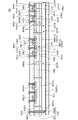
図1は、第1の実施形態に係る半導体装置SDの構成を示す断面図である。本実施形態に係る半導体装置SDは、基板SUBを用いて形成されている。基板SUBは、バルクの半導体(たとえば単結晶シリコン)からなるベース基板BSUBの上に、半導体(たとえばシリコン)のエピタキシャル層EPI(半導体層)を成長させたものである。ベース基板BSUB及びエピタキシャル層EPIは、いずれも同一の導電型(第1導電型:例えばp型)である。ベース基板BSUBの不純物濃度はエピタキシャル層EPIの不純物濃度よりも高い。
図7は、第2の実施形態に係る半導体装置SDの製造方法を示す断面図である。まず図7(a)に示すように、ベース基板BSUBを準備する。次いで、ベース基板BSUBにn型の不純物を熱拡散又はイオン注入する。これにより、ベース基板BSUBの表層には第2埋込層BINPL2が形成される。
図9は、第3の実施形態に係る半導体装置SDの構成を示す断面図である。本実施形態に係る半導体装置SDは、第2埋込層BINPL2の代わりに第3埋込層BINPL3を備えている点を除いて、第2の実施形態に係る半導体装置SDと同様の構成である。
図11は、第4の実施形態に係る半導体装置SDの構成を示す断面図である。本実施形態に係る半導体装置SDは、埋込コンタクトBCONの代わりに裏面電極BELを備えている点を除いて、第1〜第3の実施形態のいずれかと同様の構成である。本図は、第1の実施形態と同様の構成の場合を示している。
BINPL2 第2埋込層
BINSL1 埋込絶縁膜
BCON 埋込コンタクト
BINSL 埋込絶縁膜
BSUB ベース基板
CON1 第1コンタクト
DRN1 ドレイン
DRN2 ドレイン
DRN3 ドレイン
DWL ディープウェル
EL1 第1素子領域
EL2 第2素子領域
EPI エピタキシャル層
GE1 ゲート電極
GE2 ゲート電極
GE3 ゲート電極
HMSK1 絶縁膜
HINPL12 高濃度領域
HINPL13 高濃度領域
Claims (6)
- 第1導電型のベース基板と、
前記ベース基板上に形成され、前記ベース基板よりも不純物濃度が低い第1導電型の半導体層と、
前記半導体層に形成された第2導電型の第1埋込層と、
前記半導体層に形成され、前記第1埋込層よりも深く、かつ前記第1埋込層から前記半導体層の深さ方向に離れており、前記第1埋込層よりも不純物濃度が低い前記第2導電型の第2埋込層と、
前記半導体層に形成されたトランジスタと、
を備える半導体装置。 - 請求項1に記載の半導体装置において、
前記半導体層に形成され、前記トランジスタを囲むトレンチと、
前記トレンチに埋め込まれた絶縁膜と、
を備え、
前記トレンチの底面は、前記第2埋込層よりも浅く位置している半導体装置。 - 請求項1に記載の半導体装置において、
前記半導体層に形成された孔と、
前記孔の側面に形成された絶縁層と、
前記孔に埋め込まれた導体と、
を備え、
前記孔の底面は、前記第2埋込層よりも深い半導体装置。 - 請求項3に記載の半導体装置において、
前記半導体層に形成され、前記孔の底部に位置し、前記ベース基板よりも不純物濃度が高い第1導電型領域を備える半導体装置。 - 請求項1に記載の半導体装置において、
前記第2埋込層にはPが導入されており、
前記ベース基板にはBが導入されている半導体装置。 - 第1導電型のベース基板と、
前記ベース基板上に形成され、前記ベース基板よりも不純物濃度が低い第1導電型の半導体層と、
前記半導体層に形成された第2導電型の第1埋込層と、
前記半導体層に形成され、前記第1埋込層よりも深く、かつ前記第1埋込層から前記半導体層の深さ方向に離れており、N、C、及びOの少なくとも一つの元素が導入されており、前記元素の濃度が前記ベース基板における前記第1導電型の不純物濃度以下であり、かつ前記半導体層における前記第1導電型の不純物濃度よりも大きい第2埋込層と、
前記半導体層に形成されたトランジスタと、
を備える半導体装置。
Priority Applications (7)
| Application Number | Priority Date | Filing Date | Title |
|---|---|---|---|
| JP2014107950A JP6300638B2 (ja) | 2014-05-26 | 2014-05-26 | 半導体装置 |
| EP15165397.9A EP2950339A1 (en) | 2014-05-26 | 2015-04-28 | Semiconductor device |
| US14/712,894 US10062773B2 (en) | 2014-05-26 | 2015-05-14 | Semiconductor device having a transistor and first and second embedded layers |
| KR1020150071077A KR20150136015A (ko) | 2014-05-26 | 2015-05-21 | 반도체 장치 |
| TW104116362A TW201606939A (zh) | 2014-05-26 | 2015-05-22 | 半導體裝置 |
| CN201510272590.8A CN105140223A (zh) | 2014-05-26 | 2015-05-25 | 半导体器件 |
| US16/019,047 US20180308964A1 (en) | 2014-05-26 | 2018-06-26 | Semiconductor device |
Applications Claiming Priority (1)
| Application Number | Priority Date | Filing Date | Title |
|---|---|---|---|
| JP2014107950A JP6300638B2 (ja) | 2014-05-26 | 2014-05-26 | 半導体装置 |
Publications (2)
| Publication Number | Publication Date |
|---|---|
| JP2015225877A JP2015225877A (ja) | 2015-12-14 |
| JP6300638B2 true JP6300638B2 (ja) | 2018-03-28 |
Family
ID=53002622
Family Applications (1)
| Application Number | Title | Priority Date | Filing Date |
|---|---|---|---|
| JP2014107950A Active JP6300638B2 (ja) | 2014-05-26 | 2014-05-26 | 半導体装置 |
Country Status (6)
| Country | Link |
|---|---|
| US (2) | US10062773B2 (ja) |
| EP (1) | EP2950339A1 (ja) |
| JP (1) | JP6300638B2 (ja) |
| KR (1) | KR20150136015A (ja) |
| CN (1) | CN105140223A (ja) |
| TW (1) | TW201606939A (ja) |
Families Citing this family (1)
| Publication number | Priority date | Publication date | Assignee | Title |
|---|---|---|---|---|
| DE102017102127B4 (de) | 2017-02-03 | 2023-03-09 | Infineon Technologies Ag | Verfahren zum Herstellen von Halbleitervorrichtungen unter Verwendung einer Epitaxie und Halbleitervorrichtungen mit einer lateralen Struktur |
Family Cites Families (28)
| Publication number | Priority date | Publication date | Assignee | Title |
|---|---|---|---|---|
| JPS5887866A (ja) * | 1981-11-20 | 1983-05-25 | Hitachi Ltd | 半導体装置 |
| JPS6240719A (ja) | 1985-08-16 | 1987-02-21 | Nec Corp | エピタキシアルウエ−ハの製造方法 |
| JPH0364029A (ja) * | 1989-08-02 | 1991-03-19 | Hitachi Ltd | 半導体装置およびその製造方法 |
| JPH10125916A (ja) * | 1996-10-24 | 1998-05-15 | Matsushita Electric Ind Co Ltd | 半導体装置及びその製造方法 |
| JP4528460B2 (ja) * | 2000-06-30 | 2010-08-18 | 株式会社東芝 | 半導体素子 |
| JP2002134627A (ja) * | 2000-10-23 | 2002-05-10 | Sharp Corp | 半導体装置及びその製造方法 |
| JP2002176177A (ja) | 2000-12-07 | 2002-06-21 | Denso Corp | 半導体装置及びその製造方法 |
| JP4728508B2 (ja) * | 2001-06-11 | 2011-07-20 | 株式会社東芝 | 縦型電力用半導体素子の製造方法 |
| US6916330B2 (en) * | 2001-10-30 | 2005-07-12 | Depuy Spine, Inc. | Non cannulated dilators |
| US6664608B1 (en) * | 2001-11-30 | 2003-12-16 | Sun Microsystems, Inc. | Back-biased MOS device |
| US6734493B2 (en) * | 2002-02-08 | 2004-05-11 | Taiwan Semiconductor Manufacturing Co., Ltd. | Lateral double diffused metal oxide semiconductor (LDMOS) device with aligned buried layer isolation layer |
| US6943426B2 (en) * | 2002-08-14 | 2005-09-13 | Advanced Analogic Technologies, Inc. | Complementary analog bipolar transistors with trench-constrained isolation diffusion |
| JP4437388B2 (ja) * | 2003-02-06 | 2010-03-24 | 株式会社リコー | 半導体装置 |
| TWI223442B (en) * | 2003-09-02 | 2004-11-01 | Nanya Technology Corp | DRAM cell array and its manufacturing method |
| US8253196B2 (en) * | 2004-01-29 | 2012-08-28 | Enpirion, Inc. | Integrated circuit with a laterally diffused metal oxide semiconductor device and method of forming the same |
| US7714381B2 (en) * | 2005-04-01 | 2010-05-11 | Semiconductor Components Industries, Llc | Method of forming an integrated power device and structure |
| JP5164333B2 (ja) * | 2005-12-28 | 2013-03-21 | オンセミコンダクター・トレーディング・リミテッド | 半導体装置 |
| JP2007221024A (ja) * | 2006-02-20 | 2007-08-30 | Toshiba Corp | 半導体装置 |
| JP4800862B2 (ja) * | 2006-06-21 | 2011-10-26 | 株式会社日立製作所 | ファントム |
| JP4798119B2 (ja) * | 2007-11-06 | 2011-10-19 | 株式会社デンソー | 炭化珪素半導体装置およびその製造方法 |
| JP4577355B2 (ja) * | 2007-12-26 | 2010-11-10 | 株式会社デンソー | 炭化珪素半導体装置およびその製造方法 |
| US7977715B2 (en) * | 2008-03-17 | 2011-07-12 | Fairchild Semiconductor Corporation | LDMOS devices with improved architectures |
| US20110156682A1 (en) * | 2009-12-30 | 2011-06-30 | Dev Alok Girdhar | Voltage converter with integrated schottky device and systems including same |
| JP5120418B2 (ja) * | 2010-06-07 | 2013-01-16 | 富士電機株式会社 | 半導体装置 |
| CN102376548A (zh) * | 2010-08-26 | 2012-03-14 | 上海华虹Nec电子有限公司 | 降低外延工艺中自掺杂与外扩散的方法 |
| CA2812198C (en) * | 2010-10-04 | 2019-12-31 | Dana Canada Corporation | Conformal fluid-cooled heat exchanger for battery |
| JP2012169384A (ja) * | 2011-02-11 | 2012-09-06 | Denso Corp | 炭化珪素半導体装置およびその製造方法 |
| US9287371B2 (en) * | 2012-10-05 | 2016-03-15 | Semiconductor Components Industries, Llc | Semiconductor device having localized charge balance structure and method |
-
2014
- 2014-05-26 JP JP2014107950A patent/JP6300638B2/ja active Active
-
2015
- 2015-04-28 EP EP15165397.9A patent/EP2950339A1/en not_active Withdrawn
- 2015-05-14 US US14/712,894 patent/US10062773B2/en active Active
- 2015-05-21 KR KR1020150071077A patent/KR20150136015A/ko not_active Withdrawn
- 2015-05-22 TW TW104116362A patent/TW201606939A/zh unknown
- 2015-05-25 CN CN201510272590.8A patent/CN105140223A/zh active Pending
-
2018
- 2018-06-26 US US16/019,047 patent/US20180308964A1/en not_active Abandoned
Also Published As
| Publication number | Publication date |
|---|---|
| US20180308964A1 (en) | 2018-10-25 |
| US10062773B2 (en) | 2018-08-28 |
| EP2950339A1 (en) | 2015-12-02 |
| TW201606939A (zh) | 2016-02-16 |
| CN105140223A (zh) | 2015-12-09 |
| KR20150136015A (ko) | 2015-12-04 |
| JP2015225877A (ja) | 2015-12-14 |
| US20150340479A1 (en) | 2015-11-26 |
Similar Documents
| Publication | Publication Date | Title |
|---|---|---|
| TWI488297B (zh) | 元件與其形成方法 | |
| US10014406B2 (en) | Semiconductor device and method of forming the same | |
| JP6238234B2 (ja) | 半導体装置 | |
| CN205542791U (zh) | 半导体器件 | |
| CN101026192B (zh) | 半导体装置及其制造方法 | |
| TWI587402B (zh) | 高壓半導體裝置及其製造方法 | |
| JP2009055027A (ja) | Mosトランジスタの製造方法、および、これにより製造されたmosトランジスタ | |
| JP4579512B2 (ja) | 半導体装置およびその製造方法 | |
| JP2004335812A (ja) | 高耐圧半導体装置及びその製造方法 | |
| JP5378925B2 (ja) | 半導体装置およびその製造方法 | |
| JP6300638B2 (ja) | 半導体装置 | |
| JP2012160685A (ja) | 半導体装置及び半導体装置の製造方法 | |
| US10290728B2 (en) | Semiconductor device and manufacturing method thereof | |
| JP2011171602A (ja) | 半導体装置およびその製造方法 | |
| KR102178535B1 (ko) | 반도체 소자의 제조 방법 | |
| KR20140028977A (ko) | 반도체 소자 및 그 형성 방법 | |
| TWI548090B (zh) | 半導體裝置及其製作方法 | |
| TWI435449B (zh) | 溝槽式功率半導體元件及其製造方法 | |
| KR20110037031A (ko) | 반도체 소자 및 그 제조 방법 | |
| KR20100074503A (ko) | 트렌치 게이트형 모스트랜지스터의 제조방법 | |
| JP5071652B2 (ja) | 半導体装置 | |
| KR20020020175A (ko) | 반도체 장치 및 그 제조 방법 | |
| KR100799112B1 (ko) | 반도체 소자의 트랜지스터 제조 방법 | |
| JP2009164651A (ja) | 半導体装置 | |
| JP2006134947A (ja) | 半導体装置およびその製造方法 |
Legal Events
| Date | Code | Title | Description |
|---|---|---|---|
| A621 | Written request for application examination |
Free format text: JAPANESE INTERMEDIATE CODE: A621 Effective date: 20160926 |
|
| A977 | Report on retrieval |
Free format text: JAPANESE INTERMEDIATE CODE: A971007 Effective date: 20170606 |
|
| A131 | Notification of reasons for refusal |
Free format text: JAPANESE INTERMEDIATE CODE: A131 Effective date: 20170801 |
|
| A521 | Request for written amendment filed |
Free format text: JAPANESE INTERMEDIATE CODE: A523 Effective date: 20170929 |
|
| TRDD | Decision of grant or rejection written | ||
| A01 | Written decision to grant a patent or to grant a registration (utility model) |
Free format text: JAPANESE INTERMEDIATE CODE: A01 Effective date: 20180206 |
|
| A61 | First payment of annual fees (during grant procedure) |
Free format text: JAPANESE INTERMEDIATE CODE: A61 Effective date: 20180227 |
|
| R150 | Certificate of patent or registration of utility model |
Ref document number: 6300638 Country of ref document: JP Free format text: JAPANESE INTERMEDIATE CODE: R150 |
|
| R250 | Receipt of annual fees |
Free format text: JAPANESE INTERMEDIATE CODE: R250 |