KR20170077267A - 반도체 장치 - Google Patents
반도체 장치 Download PDFInfo
- Publication number
- KR20170077267A KR20170077267A KR1020177017232A KR20177017232A KR20170077267A KR 20170077267 A KR20170077267 A KR 20170077267A KR 1020177017232 A KR1020177017232 A KR 1020177017232A KR 20177017232 A KR20177017232 A KR 20177017232A KR 20170077267 A KR20170077267 A KR 20170077267A
- Authority
- KR
- South Korea
- Prior art keywords
- wiring
- transistor
- electrode
- oxide semiconductor
- insulating layer
- Prior art date
- Legal status (The legal status is an assumption and is not a legal conclusion. Google has not performed a legal analysis and makes no representation as to the accuracy of the status listed.)
- Granted
Links
Images















Classifications
-
- H—ELECTRICITY
- H10—SEMICONDUCTOR DEVICES; ELECTRIC SOLID-STATE DEVICES NOT OTHERWISE PROVIDED FOR
- H10B—ELECTRONIC MEMORY DEVICES
- H10B41/00—Electrically erasable-and-programmable ROM [EEPROM] devices comprising floating gates
- H10B41/70—Electrically erasable-and-programmable ROM [EEPROM] devices comprising floating gates the floating gate being an electrode shared by two or more components
-
- H01L27/1156—
-
- G—PHYSICS
- G11—INFORMATION STORAGE
- G11C—STATIC STORES
- G11C11/00—Digital stores characterised by the use of particular electric or magnetic storage elements; Storage elements therefor
- G11C11/21—Digital stores characterised by the use of particular electric or magnetic storage elements; Storage elements therefor using electric elements
- G11C11/34—Digital stores characterised by the use of particular electric or magnetic storage elements; Storage elements therefor using electric elements using semiconductor devices
- G11C11/40—Digital stores characterised by the use of particular electric or magnetic storage elements; Storage elements therefor using electric elements using semiconductor devices using transistors
- G11C11/401—Digital stores characterised by the use of particular electric or magnetic storage elements; Storage elements therefor using electric elements using semiconductor devices using transistors forming cells needing refreshing or charge regeneration, i.e. dynamic cells
- G11C11/403—Digital stores characterised by the use of particular electric or magnetic storage elements; Storage elements therefor using electric elements using semiconductor devices using transistors forming cells needing refreshing or charge regeneration, i.e. dynamic cells with charge regeneration common to a multiplicity of memory cells, i.e. external refresh
- G11C11/405—Digital stores characterised by the use of particular electric or magnetic storage elements; Storage elements therefor using electric elements using semiconductor devices using transistors forming cells needing refreshing or charge regeneration, i.e. dynamic cells with charge regeneration common to a multiplicity of memory cells, i.e. external refresh with three charge-transfer gates, e.g. MOS transistors, per cell
-
- G—PHYSICS
- G11—INFORMATION STORAGE
- G11C—STATIC STORES
- G11C16/00—Erasable programmable read-only memories
- G11C16/02—Erasable programmable read-only memories electrically programmable
- G11C16/04—Erasable programmable read-only memories electrically programmable using variable threshold transistors, e.g. FAMOS
- G11C16/0408—Erasable programmable read-only memories electrically programmable using variable threshold transistors, e.g. FAMOS comprising cells containing floating gate transistors
- G11C16/0433—Erasable programmable read-only memories electrically programmable using variable threshold transistors, e.g. FAMOS comprising cells containing floating gate transistors comprising cells containing a single floating gate transistor and one or more separate select transistors
-
- H01L21/8221—
-
- H01L27/1052—
-
- H01L27/11551—
-
- H01L27/11803—
-
- H01L27/1225—
-
- H01L29/7833—
-
- H01L29/7869—
-
- H—ELECTRICITY
- H10—SEMICONDUCTOR DEVICES; ELECTRIC SOLID-STATE DEVICES NOT OTHERWISE PROVIDED FOR
- H10B—ELECTRONIC MEMORY DEVICES
- H10B41/00—Electrically erasable-and-programmable ROM [EEPROM] devices comprising floating gates
- H10B41/20—Electrically erasable-and-programmable ROM [EEPROM] devices comprising floating gates characterised by three-dimensional [3D] arrangements, e.g. with cells on different height levels
-
- H—ELECTRICITY
- H10—SEMICONDUCTOR DEVICES; ELECTRIC SOLID-STATE DEVICES NOT OTHERWISE PROVIDED FOR
- H10B—ELECTRONIC MEMORY DEVICES
- H10B69/00—Erasable-and-programmable ROM [EPROM] devices not provided for in groups H10B41/00 - H10B63/00, e.g. ultraviolet erasable-and-programmable ROM [UVEPROM] devices
-
- H—ELECTRICITY
- H10—SEMICONDUCTOR DEVICES; ELECTRIC SOLID-STATE DEVICES NOT OTHERWISE PROVIDED FOR
- H10D—INORGANIC ELECTRIC SEMICONDUCTOR DEVICES
- H10D30/00—Field-effect transistors [FET]
- H10D30/60—Insulated-gate field-effect transistors [IGFET]
- H10D30/67—Thin-film transistors [TFT]
- H10D30/674—Thin-film transistors [TFT] characterised by the active materials
- H10D30/6755—Oxide semiconductors, e.g. zinc oxide, copper aluminium oxide or cadmium stannate
-
- H—ELECTRICITY
- H10—SEMICONDUCTOR DEVICES; ELECTRIC SOLID-STATE DEVICES NOT OTHERWISE PROVIDED FOR
- H10D—INORGANIC ELECTRIC SEMICONDUCTOR DEVICES
- H10D30/00—Field-effect transistors [FET]
- H10D30/60—Insulated-gate field-effect transistors [IGFET]
- H10D30/67—Thin-film transistors [TFT]
- H10D30/674—Thin-film transistors [TFT] characterised by the active materials
- H10D30/6755—Oxide semiconductors, e.g. zinc oxide, copper aluminium oxide or cadmium stannate
- H10D30/6756—Amorphous oxide semiconductors
-
- H—ELECTRICITY
- H10—SEMICONDUCTOR DEVICES; ELECTRIC SOLID-STATE DEVICES NOT OTHERWISE PROVIDED FOR
- H10D—INORGANIC ELECTRIC SEMICONDUCTOR DEVICES
- H10D30/00—Field-effect transistors [FET]
- H10D30/60—Insulated-gate field-effect transistors [IGFET]
- H10D30/67—Thin-film transistors [TFT]
- H10D30/6757—Thin-film transistors [TFT] characterised by the structure of the channel, e.g. transverse or longitudinal shape or doping profile
-
- H—ELECTRICITY
- H10—SEMICONDUCTOR DEVICES; ELECTRIC SOLID-STATE DEVICES NOT OTHERWISE PROVIDED FOR
- H10D—INORGANIC ELECTRIC SEMICONDUCTOR DEVICES
- H10D62/00—Semiconductor bodies, or regions thereof, of devices having potential barriers
- H10D62/40—Crystalline structures
- H10D62/402—Amorphous materials
-
- H—ELECTRICITY
- H10—SEMICONDUCTOR DEVICES; ELECTRIC SOLID-STATE DEVICES NOT OTHERWISE PROVIDED FOR
- H10D—INORGANIC ELECTRIC SEMICONDUCTOR DEVICES
- H10D62/00—Semiconductor bodies, or regions thereof, of devices having potential barriers
- H10D62/80—Semiconductor bodies, or regions thereof, of devices having potential barriers characterised by the materials
-
- H—ELECTRICITY
- H10—SEMICONDUCTOR DEVICES; ELECTRIC SOLID-STATE DEVICES NOT OTHERWISE PROVIDED FOR
- H10D—INORGANIC ELECTRIC SEMICONDUCTOR DEVICES
- H10D62/00—Semiconductor bodies, or regions thereof, of devices having potential barriers
- H10D62/80—Semiconductor bodies, or regions thereof, of devices having potential barriers characterised by the materials
- H10D62/83—Semiconductor bodies, or regions thereof, of devices having potential barriers characterised by the materials being Group IV materials, e.g. B-doped Si or undoped Ge
-
- H—ELECTRICITY
- H10—SEMICONDUCTOR DEVICES; ELECTRIC SOLID-STATE DEVICES NOT OTHERWISE PROVIDED FOR
- H10D—INORGANIC ELECTRIC SEMICONDUCTOR DEVICES
- H10D84/00—Integrated devices formed in or on semiconductor substrates that comprise only semiconducting layers, e.g. on Si wafers or on GaAs-on-Si wafers
- H10D84/90—Masterslice integrated circuits
- H10D84/903—Masterslice integrated circuits comprising field effect technology
-
- H—ELECTRICITY
- H10—SEMICONDUCTOR DEVICES; ELECTRIC SOLID-STATE DEVICES NOT OTHERWISE PROVIDED FOR
- H10D—INORGANIC ELECTRIC SEMICONDUCTOR DEVICES
- H10D86/00—Integrated devices formed in or on insulating or conducting substrates, e.g. formed in silicon-on-insulator [SOI] substrates or on stainless steel or glass substrates
- H10D86/40—Integrated devices formed in or on insulating or conducting substrates, e.g. formed in silicon-on-insulator [SOI] substrates or on stainless steel or glass substrates characterised by multiple TFTs
- H10D86/421—Integrated devices formed in or on insulating or conducting substrates, e.g. formed in silicon-on-insulator [SOI] substrates or on stainless steel or glass substrates characterised by multiple TFTs having a particular composition, shape or crystalline structure of the active layer
- H10D86/423—Integrated devices formed in or on insulating or conducting substrates, e.g. formed in silicon-on-insulator [SOI] substrates or on stainless steel or glass substrates characterised by multiple TFTs having a particular composition, shape or crystalline structure of the active layer comprising semiconductor materials not belonging to the Group IV, e.g. InGaZnO
-
- H—ELECTRICITY
- H10—SEMICONDUCTOR DEVICES; ELECTRIC SOLID-STATE DEVICES NOT OTHERWISE PROVIDED FOR
- H10D—INORGANIC ELECTRIC SEMICONDUCTOR DEVICES
- H10D86/00—Integrated devices formed in or on insulating or conducting substrates, e.g. formed in silicon-on-insulator [SOI] substrates or on stainless steel or glass substrates
- H10D86/40—Integrated devices formed in or on insulating or conducting substrates, e.g. formed in silicon-on-insulator [SOI] substrates or on stainless steel or glass substrates characterised by multiple TFTs
- H10D86/441—Interconnections, e.g. scanning lines
-
- H—ELECTRICITY
- H10—SEMICONDUCTOR DEVICES; ELECTRIC SOLID-STATE DEVICES NOT OTHERWISE PROVIDED FOR
- H10D—INORGANIC ELECTRIC SEMICONDUCTOR DEVICES
- H10D86/00—Integrated devices formed in or on insulating or conducting substrates, e.g. formed in silicon-on-insulator [SOI] substrates or on stainless steel or glass substrates
- H10D86/40—Integrated devices formed in or on insulating or conducting substrates, e.g. formed in silicon-on-insulator [SOI] substrates or on stainless steel or glass substrates characterised by multiple TFTs
- H10D86/481—Integrated devices formed in or on insulating or conducting substrates, e.g. formed in silicon-on-insulator [SOI] substrates or on stainless steel or glass substrates characterised by multiple TFTs integrated with passive devices, e.g. auxiliary capacitors
-
- H—ELECTRICITY
- H10—SEMICONDUCTOR DEVICES; ELECTRIC SOLID-STATE DEVICES NOT OTHERWISE PROVIDED FOR
- H10D—INORGANIC ELECTRIC SEMICONDUCTOR DEVICES
- H10D86/00—Integrated devices formed in or on insulating or conducting substrates, e.g. formed in silicon-on-insulator [SOI] substrates or on stainless steel or glass substrates
- H10D86/40—Integrated devices formed in or on insulating or conducting substrates, e.g. formed in silicon-on-insulator [SOI] substrates or on stainless steel or glass substrates characterised by multiple TFTs
- H10D86/60—Integrated devices formed in or on insulating or conducting substrates, e.g. formed in silicon-on-insulator [SOI] substrates or on stainless steel or glass substrates characterised by multiple TFTs wherein the TFTs are in active matrices
-
- H—ELECTRICITY
- H10—SEMICONDUCTOR DEVICES; ELECTRIC SOLID-STATE DEVICES NOT OTHERWISE PROVIDED FOR
- H10D—INORGANIC ELECTRIC SEMICONDUCTOR DEVICES
- H10D87/00—Integrated devices comprising both bulk components and either SOI or SOS components on the same substrate
-
- G—PHYSICS
- G11—INFORMATION STORAGE
- G11C—STATIC STORES
- G11C2211/00—Indexing scheme relating to digital stores characterized by the use of particular electric or magnetic storage elements; Storage elements therefor
- G11C2211/401—Indexing scheme relating to cells needing refreshing or charge regeneration, i.e. dynamic cells
- G11C2211/4016—Memory devices with silicon-on-insulator cells
-
- H—ELECTRICITY
- H10—SEMICONDUCTOR DEVICES; ELECTRIC SOLID-STATE DEVICES NOT OTHERWISE PROVIDED FOR
- H10B—ELECTRONIC MEMORY DEVICES
- H10B12/00—Dynamic random access memory [DRAM] devices
-
- H—ELECTRICITY
- H10—SEMICONDUCTOR DEVICES; ELECTRIC SOLID-STATE DEVICES NOT OTHERWISE PROVIDED FOR
- H10D—INORGANIC ELECTRIC SEMICONDUCTOR DEVICES
- H10D30/00—Field-effect transistors [FET]
- H10D30/60—Insulated-gate field-effect transistors [IGFET]
- H10D30/601—Insulated-gate field-effect transistors [IGFET] having lightly-doped drain or source extensions, e.g. LDD IGFETs or DDD IGFETs
-
- H—ELECTRICITY
- H10—SEMICONDUCTOR DEVICES; ELECTRIC SOLID-STATE DEVICES NOT OTHERWISE PROVIDED FOR
- H10D—INORGANIC ELECTRIC SEMICONDUCTOR DEVICES
- H10D84/00—Integrated devices formed in or on semiconductor substrates that comprise only semiconducting layers, e.g. on Si wafers or on GaAs-on-Si wafers
- H10D84/01—Manufacture or treatment
- H10D84/02—Manufacture or treatment characterised by using material-based technologies
- H10D84/03—Manufacture or treatment characterised by using material-based technologies using Group IV technology, e.g. silicon technology or silicon-carbide [SiC] technology
- H10D84/038—Manufacture or treatment characterised by using material-based technologies using Group IV technology, e.g. silicon technology or silicon-carbide [SiC] technology using silicon technology, e.g. SiGe
-
- H—ELECTRICITY
- H10—SEMICONDUCTOR DEVICES; ELECTRIC SOLID-STATE DEVICES NOT OTHERWISE PROVIDED FOR
- H10D—INORGANIC ELECTRIC SEMICONDUCTOR DEVICES
- H10D88/00—Three-dimensional [3D] integrated devices
-
- H—ELECTRICITY
- H10—SEMICONDUCTOR DEVICES; ELECTRIC SOLID-STATE DEVICES NOT OTHERWISE PROVIDED FOR
- H10D—INORGANIC ELECTRIC SEMICONDUCTOR DEVICES
- H10D88/00—Three-dimensional [3D] integrated devices
- H10D88/01—Manufacture or treatment
Landscapes
- Engineering & Computer Science (AREA)
- Microelectronics & Electronic Packaging (AREA)
- Computer Hardware Design (AREA)
- Thin Film Transistor (AREA)
- Semiconductor Memories (AREA)
- Metal-Oxide And Bipolar Metal-Oxide Semiconductor Integrated Circuits (AREA)
- Non-Volatile Memory (AREA)
- Dram (AREA)
- Physical Vapour Deposition (AREA)
Abstract
Description
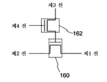
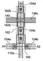
도 2a 및 도 2b는 반도체 장치를 나타내는 단면도 및 평면도이다.
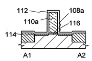
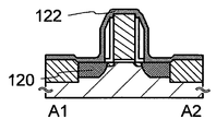
도 3a 내지 도 3h는 반도체 장치를 제작하는 단계를 나타내는 단면도이다.
도 4의 (A) 내지 (G)는 반도체 장치를 제작하는 단계를 나타내는 단면도이다.
도 5의 (A) 내지 (D)는 반도체 장치를 제작하는 단계를 나타내는 단면도이다.
도 6은 반도체 장치의 단면도이다.
도 7의 (A)와 (B)는 각각 반도체 장치를 나타내는 단면도이다.
도 8의 (A)와 (B)는 각각 반도체 장치를 나타내는 단면도이다.
도 9의 (A)와 (B)는 각각 반도체 장치를 나타내는 단면도이다.
도 10은 기억 소자의 회로도이다.
도 11은 기억 소자의 동작을 나타내는 타이밍 차트이다.
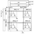
도 12는 반도체 장치의 회로도이다.
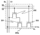
도 13은 기억 소자의 회로도이다.
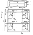
도 14는 반도체 장치의 회로도이다.
도 15는 기억 소자의 회로도이다.
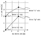
도 16은 노드 A의 전위와 제5 배선의 관계를 나타낸다.
도 17은 반도체 장치의 회로도이다.
도 18은 기억 소자의 회로도이다.
도 19는 반도체 장치의 회로도이다.
도 20a 및 도 20b는 각각 기억 소자를 나타내는 회로도이다.
도 21은 기억 소자의 회로도이다.
도 22는 판독 회로의 회로도이다.
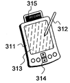
도 23a 내지 도 23f는 전자기기를 각각 나타낸다.
도 24는 산화물 반도체를 포함하는 역스태거형 트랜지스터의 단면도이다.
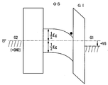
도 25a 및 도 25b는 도 24에 있어서 A-A' 단면의 에너지 밴드도(개략도)이다.
도 26a는 양의 전위(+VG)가 게이트(G1)에 인가된 상태를 나타내며, 도 26b는 음의 전위(-VG)가 게이트(G1)에 인가된 상태를 나타낸다.
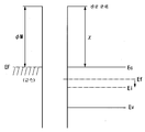
도 27은 진공 준위, 금속의 일함수(ΨM), 및 산화물 반도체의 전자 친화도(

Claims (14)
- 반도체 장치로서,
제1 배선, 제2 배선, 제3 배선, 제4 배선, 제5 배선, 및 상기 제1 배선과 상기 제2 배선 사이에 병렬로 접속되는 복수의 기억 소자
를 포함하고,
상기 복수의 기억 소자 중 하나는, 제1 게이트 전극, 제1 소스 전극, 및 제1 드레인 전극을 갖는 제1 트랜지스터; 제2 게이트 전극, 제2 소스 전극, 및 제2 드레인 전극을 갖는 제2 트랜지스터; 제3 게이트 전극, 제3 소스 전극, 및 제3 드레인 전극을 갖는 제3 트랜지스터; 및 용량 소자를 포함하며,
상기 제2 트랜지스터는 산화물 반도체 재료를 포함하고,
상기 제1 게이트 전극과, 상기 제2 소스 전극 및 상기 제2 드레인 전극 중 하나와, 상기 용량 소자의 전극 중 하나는 서로 전기적으로 접속되고,
상기 제1 배선과, 상기 제1 소스 전극과, 상기 용량 소자의 상기 전극 중 다른 하나는 서로 전기적으로 접속되고,
상기 제1 드레인 전극과 상기 제3 소스 전극은 서로 전기적으로 접속되고,
상기 제2 배선과 상기 제3 드레인 전극은 서로 전기적으로 접속되고,
상기 제3 배선과, 상기 제2 소스 전극 및 상기 제2 드레인 전극 중 다른 하나는 서로 전기적으로 접속되고,
상기 제4 배선과 상기 제2 게이트 전극은 서로 전기적으로 접속되고,
상기 제5 배선과 상기 제3 게이트 전극은 서로 전기적으로 접속되는, 반도체 장치. - 반도체 장치로서,
제1 배선, 제2 배선, 제3 배선, 제4 배선, 제5 배선, 및 상기 제1 배선과 상기 제2 배선 사이에 병렬로 접속되는 복수의 기억 소자
를 포함하고,
상기 복수의 기억 소자 중 하나는, 제1 게이트 전극, 제1 소스 전극, 및 제1 드레인 전극을 갖는 제1 트랜지스터; 제2 게이트 전극, 제2 소스 전극, 및 제2 드레인 전극을 갖는 제2 트랜지스터; 제3 게이트 전극, 제3 소스 전극, 및 제3 드레인 전극을 갖는 제3 트랜지스터; 및 용량 소자를 포함하며,
상기 제2 트랜지스터는 산화물 반도체 재료를 포함하고,
상기 제1 트랜지스터는 상기 제2 트랜지스터의 상기 산화물 반도체 재료가 아닌 반도체 재료를 포함하고,
상기 제1 게이트 전극과, 상기 제2 소스 전극 및 상기 제2 드레인 전극 중 하나와, 상기 용량 소자의 전극 중 하나는 서로 전기적으로 접속되고,
상기 제1 배선과, 상기 제1 소스 전극과 상기 용량 소자의 상기 전극 중 다른 하나는 서로 전기적으로 접속되고,
상기 제1 드레인 전극과 상기 제3 소스 전극은 서로 전기적으로 접속되고,
상기 제2 배선과 상기 제3 드레인 전극은 서로 전기적으로 접속되고,
상기 제3 배선과, 상기 제2 소스 전극 및 상기 제2 드레인 전극 중 다른 하나는 서로 전기적으로 접속되고,
상기 제4 배선과 상기 제2 게이트 전극은 서로 전기적으로 접속되고,
상기 제5 배선과 상기 제3 게이트 전극은 서로 전기적으로 접속되는, 반도체 장치. - 반도체 장치로서,
제1 배선, 제2 배선, 제3 배선, 제4 배선, 제5 배선, 및 상기 제1 배선과 상기 제2 배선 사이에 병렬로 접속되는 복수의 기억 소자
를 포함하고,
상기 복수의 기억 소자 중 하나는, 제1 게이트 전극, 제1 소스 전극, 및 제1 드레인 전극을 갖는 제1 트랜지스터; 제2 게이트 전극, 제2 소스 전극, 및 제2 드레인 전극을 갖는 제2 트랜지스터; 제3 게이트 전극, 제3 소스 전극, 및 제3 드레인 전극을 갖는 제3 트랜지스터; 및 용량 소자를 포함하며,
상기 제1 트랜지스터는 상기 제2 트랜지스터와 상이한 반도체 재료를 포함하고,
상기 제2 트랜지스터는 산화물 반도체 재료를 포함하고,
상기 제1 게이트 전극과, 상기 제2 소스 전극 및 상기 제2 드레인 전극 중 하나와, 상기 용량 소자의 전극 중 하나는 서로 전기적으로 접속되고,
상기 제1 배선과, 상기 제1 소스 전극과, 상기 용량 소자의 상기 전극 중 다른 하나는 서로 전기적으로 접속되고,
상기 제1 드레인 전극과 상기 제3 소스 전극은 서로 전기적으로 접속되고,
상기 제2 배선과 상기 제3 드레인 전극은 서로 전기적으로 접속되고,
상기 제3 배선과, 상기 제2 소스 전극 및 상기 제2 드레인 전극 중 다른 하나는 서로 전기적으로 접속되고,
상기 제4 배선과 상기 제2 게이트 전극은 서로 전기적으로 접속되고,
상기 제5 배선과 상기 제3 게이트 전극은 서로 전기적으로 접속되는, 반도체 장치. - 제1항 내지 제3항 중 어느 한 항에 있어서,
상기 제1 트랜지스터의 채널 영역은 산화물 재료를 포함하는 기판에 제공되는, 반도체 장치 - 제1항 내지 제3항 중 어느 한 항에 있어서,
상기 제3 트랜지스터는, 기판에 제공되는 채널 영역, 상기 채널 영역을 개재하도록 제공되는 불순물 영역들, 상기 채널 영역 위의 제3 게이트 절연층, 상기 제3 게이트 절연층 위의 상기 제3 게이트 전극, 및 상기 불순물 영역들에 전기적으로 접속되는 상기 제3 소스 전극 및 상기 제3 드레인 전극을 포함하는, 반도체 장치. - 제1항 내지 제3항 중 어느 한 항에 있어서,
산화물 재료를 포함하는 기판을 더 포함하고,
상기 제2 트랜지스터는, 상기 제2 게이트 전극 위의 제2 게이트 절연층, 상기 제2 게이트 절연층 위의 상기 산화물 반도체 재료를 포함하는 상기 산화물 반도체층, 및 상기 산화물 반도체층에 전기적으로 접속되는 상기 제2 소스 전극 및 상기 제2 드레인 전극을 포함하고,
상기 제2 게이트 전극은 상기 기판 위에 위치하는, 반도체 장치. - 제1항 내지 제3항 중 어느 한 항에 있어서,
단결정 반도체 기판 및 SOI 기판 중 하나를 더 포함하는, 반도체 장치. - 제2항 또는 제3항에 있어서,
상기 반도체 재료는 실리콘인, 반도체 장치. - 제1항 내지 제3항 중 어느 한 항에 있어서,
상기 산화물 반도체 재료는 In-Ga-Zn-O 계의 산화물 반도체 재료인, 반도체 장치. - 제1항 내지 제3항 중 어느 한 항에 있어서,
상기 산화물 반도체 재료는 In2Ga2ZnO7의 결정을 포함하는, 반도체 장치. - 제6항에 있어서,
상기 산화물 반도체층의 수소의 농도는 5×10¹⁹/cm3 이하인, 반도체 장치. - 제1항 내지 제3항 중 어느 한 항에 있어서,
상기 제2 트랜지스터의 오프 상태 전류는 1×10-13A 이하인, 반도체 장치. - 제1항 내지 제3항 중 어느 한 항에 있어서,
절연막과 상기 산화물 반도체 재료를 포함하는 산화물 반도체층을 더 포함하고,
상기 절연막은 상기 제1 게이트 전극, 상기 제1 소스 전극 및 상기 제1 드레인 전극 각각의 위에 위치하고,
상기 산화물 반도체층은 상기 절연막 위에 있는, 반도체 장치. - 제6항에 있어서,
상기 제1 트랜지스터 위에 순서대로 적층된 제1 절연층 내지 제4 절연층을 더 포함하고,
상기 산화물 반도체층은 상기 제2 절연층과 상기 제3 절연층 사이에 위치하고,
상기 제1 절연층 및 상기 제4 절연층은 각각 산화 알루미늄을 포함하고,
상기 제2 절연층 및 상기 제3 절연층은 각각 산화 실리콘, 산화 질화 실리콘, 및 질화 산화 실리콘 중 하나를 포함하는, 반도체 장치.
Applications Claiming Priority (3)
| Application Number | Priority Date | Filing Date | Title |
|---|---|---|---|
| JP2009251261 | 2009-10-30 | ||
| JPJP-P-2009-251261 | 2009-10-30 | ||
| PCT/JP2010/068647 WO2011052488A1 (en) | 2009-10-30 | 2010-10-15 | Semiconductor device |
Related Parent Applications (1)
| Application Number | Title | Priority Date | Filing Date |
|---|---|---|---|
| KR1020127010574A Division KR101752518B1 (ko) | 2009-10-30 | 2010-10-15 | 반도체 장치 |
Publications (2)
| Publication Number | Publication Date |
|---|---|
| KR20170077267A true KR20170077267A (ko) | 2017-07-05 |
| KR101788521B1 KR101788521B1 (ko) | 2017-10-19 |
Family
ID=43921911
Family Applications (2)
| Application Number | Title | Priority Date | Filing Date |
|---|---|---|---|
| KR1020177017232A Active KR101788521B1 (ko) | 2009-10-30 | 2010-10-15 | 반도체 장치 |
| KR1020127010574A Expired - Fee Related KR101752518B1 (ko) | 2009-10-30 | 2010-10-15 | 반도체 장치 |
Family Applications After (1)
| Application Number | Title | Priority Date | Filing Date |
|---|---|---|---|
| KR1020127010574A Expired - Fee Related KR101752518B1 (ko) | 2009-10-30 | 2010-10-15 | 반도체 장치 |
Country Status (7)
| Country | Link |
|---|---|
| US (11) | US8896042B2 (ko) |
| EP (1) | EP2494599B1 (ko) |
| JP (12) | JP5611764B2 (ko) |
| KR (2) | KR101788521B1 (ko) |
| CN (2) | CN102576708B (ko) |
| TW (4) | TWI574388B (ko) |
| WO (1) | WO2011052488A1 (ko) |
Families Citing this family (108)
| Publication number | Priority date | Publication date | Assignee | Title |
|---|---|---|---|---|
| JPS6093532A (ja) * | 1983-10-27 | 1985-05-25 | Matsushita Electric Ind Co Ltd | 基準電圧回路 |
| KR20190006091A (ko) | 2009-10-29 | 2019-01-16 | 가부시키가이샤 한도오따이 에네루기 켄큐쇼 | 반도체 장치 |
| WO2011052488A1 (en) | 2009-10-30 | 2011-05-05 | Semiconductor Energy Laboratory Co., Ltd. | Semiconductor device |
| EP2494597A4 (en) | 2009-10-30 | 2015-03-18 | Semiconductor Energy Lab | SEMICONDUCTOR COMPONENT |
| CN104681079B (zh) | 2009-11-06 | 2018-02-02 | 株式会社半导体能源研究所 | 半导体装置及用于驱动半导体装置的方法 |
| WO2011058934A1 (en) * | 2009-11-13 | 2011-05-19 | Semiconductor Energy Laboratory Co., Ltd. | Semiconductor device and driving method thereof |
| KR20190124813A (ko) | 2009-11-20 | 2019-11-05 | 가부시키가이샤 한도오따이 에네루기 켄큐쇼 | 반도체 장치 |
| KR101790365B1 (ko) | 2009-11-20 | 2017-10-25 | 가부시키가이샤 한도오따이 에네루기 켄큐쇼 | 반도체 장치 |
| WO2011065183A1 (en) | 2009-11-24 | 2011-06-03 | Semiconductor Energy Laboratory Co., Ltd. | Semiconductor device including memory cell |
| KR101813460B1 (ko) | 2009-12-18 | 2017-12-29 | 가부시키가이샤 한도오따이 에네루기 켄큐쇼 | 반도체 장치 |
| KR101870119B1 (ko) | 2009-12-25 | 2018-06-25 | 가부시키가이샤 한도오따이 에네루기 켄큐쇼 | 반도체 장치 |
| EP3550604A1 (en) * | 2009-12-25 | 2019-10-09 | Semiconductor Energy Laboratory Co., Ltd. | Semiconductor device |
| US8780629B2 (en) | 2010-01-15 | 2014-07-15 | Semiconductor Energy Laboratory Co., Ltd. | Semiconductor device and driving method thereof |
| KR101798367B1 (ko) | 2010-01-15 | 2017-11-16 | 가부시키가이샤 한도오따이 에네루기 켄큐쇼 | 반도체 장치 |
| US8415731B2 (en) | 2010-01-20 | 2013-04-09 | Semiconductor Energy Laboratory Co., Ltd. | Semiconductor storage device with integrated capacitor and having transistor overlapping sections |
| WO2011089852A1 (en) | 2010-01-22 | 2011-07-28 | Semiconductor Energy Laboratory Co., Ltd. | Semiconductor memory device and driving method thereof |
| WO2011129233A1 (en) | 2010-04-16 | 2011-10-20 | Semiconductor Energy Laboratory Co., Ltd. | Semiconductor device |
| US8664658B2 (en) | 2010-05-14 | 2014-03-04 | Semiconductor Energy Laboratory Co., Ltd. | Semiconductor device |
| WO2012002186A1 (en) | 2010-07-02 | 2012-01-05 | Semiconductor Energy Laboratory Co., Ltd. | Semiconductor device |
| TWI545587B (zh) * | 2010-08-06 | 2016-08-11 | 半導體能源研究所股份有限公司 | 半導體裝置及驅動半導體裝置的方法 |
| US9343480B2 (en) * | 2010-08-16 | 2016-05-17 | Semiconductor Energy Laboratory Co., Ltd. | Semiconductor device |
| JP2012256821A (ja) | 2010-09-13 | 2012-12-27 | Semiconductor Energy Lab Co Ltd | 記憶装置 |
| TWI539453B (zh) | 2010-09-14 | 2016-06-21 | 半導體能源研究所股份有限公司 | 記憶體裝置和半導體裝置 |
| JP5908263B2 (ja) | 2010-12-03 | 2016-04-26 | 株式会社半導体エネルギー研究所 | Dc−dcコンバータ |
| CN103339715B (zh) * | 2010-12-03 | 2016-01-13 | 株式会社半导体能源研究所 | 氧化物半导体膜以及半导体装置 |
| US9443984B2 (en) | 2010-12-28 | 2016-09-13 | Semiconductor Energy Laboratory Co., Ltd. | Semiconductor device and manufacturing method thereof |
| US8421071B2 (en) * | 2011-01-13 | 2013-04-16 | Semiconductor Energy Laboratory Co., Ltd. | Memory device |
| US8659957B2 (en) * | 2011-03-07 | 2014-02-25 | Semiconductor Energy Laboratory Co., Ltd. | Semiconductor device and method of driving semiconductor device |
| JP2012209543A (ja) * | 2011-03-11 | 2012-10-25 | Semiconductor Energy Lab Co Ltd | 半導体装置 |
| US8743590B2 (en) * | 2011-04-08 | 2014-06-03 | Semiconductor Energy Laboratory Co., Ltd. | Memory device and semiconductor device using the same |
| TWI570891B (zh) | 2011-05-17 | 2017-02-11 | 半導體能源研究所股份有限公司 | 半導體裝置 |
| US8779799B2 (en) * | 2011-05-19 | 2014-07-15 | Semiconductor Energy Laboratory Co., Ltd. | Logic circuit |
| US9762246B2 (en) | 2011-05-20 | 2017-09-12 | Semiconductor Energy Laboratory Co., Ltd. | Semiconductor device with a storage circuit having an oxide semiconductor |
| TWI616873B (zh) * | 2011-05-20 | 2018-03-01 | 半導體能源研究所股份有限公司 | 儲存裝置及信號處理電路 |
| JP6231735B2 (ja) * | 2011-06-01 | 2017-11-15 | 株式会社半導体エネルギー研究所 | 半導体装置 |
| US8804405B2 (en) * | 2011-06-16 | 2014-08-12 | Semiconductor Energy Laboratory Co., Ltd. | Memory device and semiconductor device |
| US9166055B2 (en) * | 2011-06-17 | 2015-10-20 | Semiconductor Energy Laboratory Co., Ltd. | Semiconductor device and method for manufacturing the same |
| US9001564B2 (en) * | 2011-06-29 | 2015-04-07 | Semiconductor Energy Laboratory Co., Ltd. | Semiconductor device and a method for driving the same |
| JP6013685B2 (ja) * | 2011-07-22 | 2016-10-25 | 株式会社半導体エネルギー研究所 | 半導体装置 |
| JP5837387B2 (ja) * | 2011-10-11 | 2015-12-24 | ルネサスエレクトロニクス株式会社 | 半導体集積回路装置および半導体集積回路装置の製造方法 |
| JP6081162B2 (ja) * | 2011-11-30 | 2017-02-15 | 株式会社半導体エネルギー研究所 | 駆動回路及び該駆動回路を具備する表示装置 |
| WO2013080900A1 (en) * | 2011-12-02 | 2013-06-06 | Semiconductor Energy Laboratory Co., Ltd. | Semiconductor device and method for manufacturing the same |
| JP6081171B2 (ja) | 2011-12-09 | 2017-02-15 | 株式会社半導体エネルギー研究所 | 記憶装置 |
| JP2013168926A (ja) * | 2012-01-18 | 2013-08-29 | Semiconductor Energy Lab Co Ltd | 回路、センサ回路及びセンサ回路を用いた半導体装置 |
| JP6125850B2 (ja) * | 2012-02-09 | 2017-05-10 | 株式会社半導体エネルギー研究所 | 半導体装置及び半導体装置の作製方法 |
| US9312257B2 (en) * | 2012-02-29 | 2016-04-12 | Semiconductor Energy Laboratory Co., Ltd. | Semiconductor device |
| JP6046514B2 (ja) | 2012-03-01 | 2016-12-14 | 株式会社半導体エネルギー研究所 | 半導体装置 |
| US9287370B2 (en) * | 2012-03-02 | 2016-03-15 | Semiconductor Energy Laboratory Co., Ltd. | Memory device comprising a transistor including an oxide semiconductor and semiconductor device including the same |
| JP2013236068A (ja) | 2012-04-12 | 2013-11-21 | Semiconductor Energy Lab Co Ltd | 半導体装置及び半導体装置の作製方法 |
| US9208849B2 (en) | 2012-04-12 | 2015-12-08 | Semiconductor Energy Laboratory Co., Ltd. | Semiconductor device and method for driving semiconductor device, and electronic device |
| KR102932705B1 (ko) * | 2012-04-13 | 2026-02-27 | 가부시키가이샤 한도오따이 에네루기 켄큐쇼 | 반도체 장치 |
| CN104321967B (zh) * | 2012-05-25 | 2018-01-09 | 株式会社半导体能源研究所 | 可编程逻辑装置及半导体装置 |
| US20130326151A1 (en) * | 2012-05-31 | 2013-12-05 | Semiconductor Energy Laboratory Co., Ltd. | Memory management system and program |
| US9312390B2 (en) * | 2012-07-05 | 2016-04-12 | Semiconductor Energy Laboratory Co., Ltd. | Remote control system |
| JP5960000B2 (ja) * | 2012-09-05 | 2016-08-02 | ルネサスエレクトロニクス株式会社 | 半導体装置及び半導体装置の製造方法 |
| TWI671910B (zh) * | 2012-09-24 | 2019-09-11 | 日商半導體能源研究所股份有限公司 | 半導體裝置 |
| JP6026844B2 (ja) * | 2012-10-17 | 2016-11-16 | 株式会社半導体エネルギー研究所 | 半導体装置 |
| TWI613813B (zh) | 2012-11-16 | 2018-02-01 | 半導體能源研究所股份有限公司 | 半導體裝置 |
| JP6113500B2 (ja) * | 2012-12-27 | 2017-04-12 | ルネサスエレクトロニクス株式会社 | 半導体装置及び半導体装置の製造方法 |
| US9286953B2 (en) * | 2013-02-28 | 2016-03-15 | Semiconductor Energy Laboratory Co., Ltd. | Semiconductor device and electronic device |
| KR102442752B1 (ko) | 2013-05-20 | 2022-09-14 | 가부시키가이샤 한도오따이 에네루기 켄큐쇼 | 반도체 장치 |
| TWI618081B (zh) | 2013-05-30 | 2018-03-11 | 半導體能源研究所股份有限公司 | 半導體裝置的驅動方法 |
| TWI641112B (zh) | 2013-06-13 | 2018-11-11 | 半導體能源研究所股份有限公司 | 半導體裝置 |
| TWI633650B (zh) * | 2013-06-21 | 2018-08-21 | 半導體能源研究所股份有限公司 | 半導體裝置 |
| JP6516978B2 (ja) | 2013-07-17 | 2019-05-22 | 株式会社半導体エネルギー研究所 | 半導体装置 |
| JP6345544B2 (ja) * | 2013-09-05 | 2018-06-20 | 株式会社半導体エネルギー研究所 | 半導体装置の作製方法 |
| JP6570817B2 (ja) * | 2013-09-23 | 2019-09-04 | 株式会社半導体エネルギー研究所 | 半導体装置 |
| JP2015084418A (ja) | 2013-09-23 | 2015-04-30 | 株式会社半導体エネルギー研究所 | 半導体装置 |
| KR102267237B1 (ko) | 2014-03-07 | 2021-06-18 | 가부시키가이샤 한도오따이 에네루기 켄큐쇼 | 반도체 장치 및 전자 기기 |
| US9842842B2 (en) | 2014-03-19 | 2017-12-12 | Semiconductor Energy Laboratory Co., Ltd. | Semiconductor memory device and semiconductor device and electronic device having the same |
| JP6525722B2 (ja) * | 2014-05-29 | 2019-06-05 | 株式会社半導体エネルギー研究所 | 記憶装置、電子部品、及び電子機器 |
| US9424890B2 (en) | 2014-12-01 | 2016-08-23 | Semiconductor Energy Laboratory Co., Ltd. | Semiconductor device and driving method thereof |
| JP2016225613A (ja) * | 2015-05-26 | 2016-12-28 | 株式会社半導体エネルギー研究所 | 半導体装置及び半導体装置の駆動方法 |
| JP2017041877A (ja) | 2015-08-21 | 2017-02-23 | 株式会社半導体エネルギー研究所 | 半導体装置、電子部品、および電子機器 |
| KR102447178B1 (ko) * | 2015-09-01 | 2022-09-26 | 삼성전자주식회사 | 반도체 장치의 제조 방법 |
| US9773787B2 (en) | 2015-11-03 | 2017-09-26 | Semiconductor Energy Laboratory Co., Ltd. | Semiconductor device, memory device, electronic device, or method for driving the semiconductor device |
| WO2017130082A1 (en) | 2016-01-29 | 2017-08-03 | Semiconductor Energy Laboratory Co., Ltd. | Semiconductor device, electronic component, and electronic device |
| CN107170681B (zh) * | 2016-03-03 | 2019-10-25 | 上海新昇半导体科技有限公司 | 真空管闪存结构之制造方法 |
| US10008502B2 (en) * | 2016-05-04 | 2018-06-26 | Semiconductor Energy Laboratory Co., Ltd. | Memory device |
| EP3463441B1 (en) | 2016-06-07 | 2023-10-25 | The General Hospital Corporation | Identification of a t cell epitope of prevotella copri that induces t cell responses in patients with rheumatoid arthritis |
| KR102458660B1 (ko) | 2016-08-03 | 2022-10-26 | 가부시키가이샤 한도오따이 에네루기 켄큐쇼 | 표시 장치 및 전자 기기 |
| US10147722B2 (en) * | 2016-08-12 | 2018-12-04 | Renesas Electronics America Inc. | Isolated circuit formed during back end of line process |
| TWI840104B (zh) | 2016-08-29 | 2024-04-21 | 日商半導體能源研究所股份有限公司 | 顯示裝置及控制程式 |
| WO2018047035A1 (en) | 2016-09-12 | 2018-03-15 | Semiconductor Energy Laboratory Co., Ltd. | Memory device, driving method thereof, semiconductor device, electronic component, and electronic device |
| JP6985092B2 (ja) | 2016-10-13 | 2021-12-22 | 株式会社半導体エネルギー研究所 | デコーダ、受信装置および電子機器 |
| JP6495878B2 (ja) * | 2016-10-13 | 2019-04-03 | 株式会社半導体エネルギー研究所 | 半導体装置 |
| WO2018073708A1 (en) | 2016-10-20 | 2018-04-26 | Semiconductor Energy Laboratory Co., Ltd. | Storage device, driving method thereof, semiconductor device, electronic component, and electronic device |
| US10223194B2 (en) | 2016-11-04 | 2019-03-05 | Semiconductor Energy Laboratory Co., Ltd. | Storage device, semiconductor device, electronic device, and server system |
| CN106531746A (zh) * | 2016-11-30 | 2017-03-22 | 京东方科技集团股份有限公司 | 一种阵列基板、阵列基板的制作方法、显示面板及显示装置 |
| US11152366B2 (en) | 2017-06-08 | 2021-10-19 | Semiconductor Energy Laboratory Co., Ltd. | Semiconductor device and method for driving semiconductor device |
| US10714400B2 (en) | 2017-08-30 | 2020-07-14 | Micron Technology, Inc. | Methods of forming semiconductor structures comprising thin film transistors including oxide semiconductors |
| WO2019102315A1 (en) * | 2017-11-23 | 2019-05-31 | Semiconductor Energy Laboratory Co., Ltd. | Display device and electronic device |
| CN111316423B (zh) * | 2017-11-24 | 2025-02-14 | 株式会社半导体能源研究所 | 半导体装置及动态逻辑电路 |
| CN110858035B (zh) * | 2018-08-24 | 2022-12-02 | 夏普株式会社 | 液晶显示装置 |
| WO2020128676A1 (ja) | 2018-12-21 | 2020-06-25 | 株式会社半導体エネルギー研究所 | 半導体装置、及びその動作方法、並びに電子機器 |
| US10892264B2 (en) | 2018-12-26 | 2021-01-12 | Micron Technology, Inc. | Memory device having 2-transistor vertical memory cell |
| CN118488706A (zh) * | 2018-12-26 | 2024-08-13 | 美光科技公司 | 具有用于2晶体管垂直存储器单元的共享读取/写入存取线的存储器装置 |
| WO2020139847A1 (en) * | 2018-12-26 | 2020-07-02 | Micron Technology, Inc. | Memory device having shared read/write data line for 2-transistor vertical memory cell |
| CN113383417B (zh) | 2018-12-26 | 2025-01-10 | 美光科技公司 | 具有用于2晶体管竖直存储器单元的共享存取线的存储器装置 |
| TWI907464B (zh) | 2020-08-12 | 2025-12-11 | 日商半導體能源研究所股份有限公司 | 顯示裝置、其工作方法以及電子裝置 |
| WO2022043826A1 (ja) | 2020-08-27 | 2022-03-03 | 株式会社半導体エネルギー研究所 | 半導体装置、表示装置、及び電子機器 |
| JP7766037B2 (ja) | 2020-09-22 | 2025-11-07 | 株式会社半導体エネルギー研究所 | 記憶装置 |
| KR20240006569A (ko) * | 2021-05-10 | 2024-01-15 | 가부시키가이샤 한도오따이 에네루기 켄큐쇼 | 반도체 장치 |
| CN115411052B (zh) * | 2021-05-10 | 2026-04-21 | 中芯国际集成电路制造(上海)有限公司 | 半导体结构及其形成方法、电路及电路工作方法 |
| JP2023023637A (ja) * | 2021-08-05 | 2023-02-16 | キオクシア株式会社 | 半導体装置及びその製造方法 |
| KR20240093546A (ko) | 2021-10-27 | 2024-06-24 | 가부시키가이샤 한도오따이 에네루기 켄큐쇼 | 표시 장치 |
| US12451431B2 (en) * | 2022-05-02 | 2025-10-21 | International Business Machines Corporation | Stacked semiconductor devices with topside and backside interconnect wiring |
| CN119031708A (zh) * | 2024-08-19 | 2024-11-26 | 北京大学 | 一种基于非对称源漏接触氧化物半导体晶体管的dram单元 |
Family Cites Families (195)
| Publication number | Priority date | Publication date | Assignee | Title |
|---|---|---|---|---|
| EP0053878B1 (en) * | 1980-12-08 | 1985-08-14 | Kabushiki Kaisha Toshiba | Semiconductor memory device |
| JPS6034199B2 (ja) | 1980-12-20 | 1985-08-07 | 株式会社東芝 | 半導体記憶装置 |
| JPS60198861A (ja) | 1984-03-23 | 1985-10-08 | Fujitsu Ltd | 薄膜トランジスタ |
| JPH0612799B2 (ja) * | 1986-03-03 | 1994-02-16 | 三菱電機株式会社 | 積層型半導体装置およびその製造方法 |
| JPS62274773A (ja) * | 1986-05-23 | 1987-11-28 | Hitachi Ltd | 半導体記憶装置 |
| JPS6370558A (ja) * | 1986-09-12 | 1988-03-30 | Nec Corp | 半導体メモリセル |
| JPH0244256B2 (ja) | 1987-01-28 | 1990-10-03 | Kagaku Gijutsucho Mukizaishitsu Kenkyushocho | Ingazn2o5deshimesarerurotsuhoshokeinosojokozoojusurukagobutsuoyobisonoseizoho |
| JPH0244258B2 (ja) | 1987-02-24 | 1990-10-03 | Kagaku Gijutsucho Mukizaishitsu Kenkyushocho | Ingazn3o6deshimesarerurotsuhoshokeinosojokozoojusurukagobutsuoyobisonoseizoho |
| JPS63210023A (ja) | 1987-02-24 | 1988-08-31 | Natl Inst For Res In Inorg Mater | InGaZn↓4O↓7で示される六方晶系の層状構造を有する化合物およびその製造法 |
| JPH0244260B2 (ja) | 1987-02-24 | 1990-10-03 | Kagaku Gijutsucho Mukizaishitsu Kenkyushocho | Ingazn5o8deshimesarerurotsuhoshokeinosojokozoojusurukagobutsuoyobisonoseizoho |
| JPH0244262B2 (ja) | 1987-02-27 | 1990-10-03 | Kagaku Gijutsucho Mukizaishitsu Kenkyushocho | Ingazn6o9deshimesarerurotsuhoshokeinosojokozoojusurukagobutsuoyobisonoseizoho |
| JPH0244263B2 (ja) | 1987-04-22 | 1990-10-03 | Kagaku Gijutsucho Mukizaishitsu Kenkyushocho | Ingazn7o10deshimesarerurotsuhoshokeinosojokozoojusurukagobutsuoyobisonoseizoho |
| US5366922A (en) * | 1989-12-06 | 1994-11-22 | Seiko Instruments Inc. | Method for producing CMOS transistor |
| JP2993039B2 (ja) * | 1990-04-13 | 1999-12-20 | 日本電気株式会社 | 能動層積層素子 |
| JP2775040B2 (ja) * | 1991-10-29 | 1998-07-09 | 株式会社 半導体エネルギー研究所 | 電気光学表示装置およびその駆動方法 |
| JPH05251705A (ja) | 1992-03-04 | 1993-09-28 | Fuji Xerox Co Ltd | 薄膜トランジスタ |
| JP3479375B2 (ja) | 1995-03-27 | 2003-12-15 | 科学技術振興事業団 | 亜酸化銅等の金属酸化物半導体による薄膜トランジスタとpn接合を形成した金属酸化物半導体装置およびそれらの製造方法 |
| JPH11505377A (ja) * | 1995-08-03 | 1999-05-18 | フィリップス エレクトロニクス ネムローゼ フェンノートシャップ | 半導体装置 |
| JP3392604B2 (ja) * | 1995-11-14 | 2003-03-31 | 株式会社東芝 | 不揮発性半導体記憶装置 |
| JP3625598B2 (ja) * | 1995-12-30 | 2005-03-02 | 三星電子株式会社 | 液晶表示装置の製造方法 |
| KR100234700B1 (ko) * | 1996-11-27 | 1999-12-15 | 김영환 | 반도체 소자의 제조방법 |
| KR100219519B1 (ko) * | 1997-01-10 | 1999-09-01 | 윤종용 | 페로일렉트릭 플로팅 게이트 램을 구비하는 반도체 메모리 디바이스 및 그 제조방법 |
| US6462193B1 (en) * | 1997-02-21 | 2002-10-08 | The Scripps Research Institute | Hydroxyazepanes as inhibitors of glycosidase and HIV protease |
| JPH10284696A (ja) | 1997-04-02 | 1998-10-23 | Nissan Motor Co Ltd | 半導体記憶装置 |
| US5796650A (en) * | 1997-05-19 | 1998-08-18 | Lsi Logic Corporation | Memory circuit including write control unit wherein subthreshold leakage may be reduced |
| JPH11126491A (ja) * | 1997-08-20 | 1999-05-11 | Fujitsu Ltd | 半導体記憶装置 |
| JPH11120797A (ja) * | 1997-10-15 | 1999-04-30 | Toshiba Microelectronics Corp | 強誘電体メモリ及びそのスクリーニング方法 |
| US5943270A (en) * | 1997-11-26 | 1999-08-24 | Intel Corporation | Two-transistor DRAM cell for logic process technology |
| JP4170454B2 (ja) | 1998-07-24 | 2008-10-22 | Hoya株式会社 | 透明導電性酸化物薄膜を有する物品及びその製造方法 |
| JP3606543B2 (ja) * | 1998-09-02 | 2005-01-05 | ローム株式会社 | 強誘電体を用いた順序回路およびこれを用いた半導体装置 |
| JP2000150861A (ja) * | 1998-11-16 | 2000-05-30 | Tdk Corp | 酸化物薄膜 |
| JP3276930B2 (ja) * | 1998-11-17 | 2002-04-22 | 科学技術振興事業団 | トランジスタ及び半導体装置 |
| JP3936830B2 (ja) | 1999-05-13 | 2007-06-27 | 株式会社日立製作所 | 半導体装置 |
| TW461096B (en) | 1999-05-13 | 2001-10-21 | Hitachi Ltd | Semiconductor memory |
| JP2001093988A (ja) * | 1999-07-22 | 2001-04-06 | Sony Corp | 半導体記憶装置 |
| JP2001053167A (ja) * | 1999-08-04 | 2001-02-23 | Sony Corp | 半導体記憶装置 |
| TW460731B (en) * | 1999-09-03 | 2001-10-21 | Ind Tech Res Inst | Electrode structure and production method of wide viewing angle LCD |
| JP4282197B2 (ja) * | 2000-01-24 | 2009-06-17 | 株式会社ルネサステクノロジ | 不揮発性半導体記憶装置 |
| US6570206B1 (en) * | 2000-03-29 | 2003-05-27 | Hitachi, Ltd. | Semiconductor device |
| US6266269B1 (en) * | 2000-06-07 | 2001-07-24 | Xilinx, Inc. | Three terminal non-volatile memory element |
| US6628551B2 (en) * | 2000-07-14 | 2003-09-30 | Infineon Technologies Aktiengesellschaft | Reducing leakage current in memory cells |
| JP4089858B2 (ja) | 2000-09-01 | 2008-05-28 | 国立大学法人東北大学 | 半導体デバイス |
| JP2002093924A (ja) | 2000-09-20 | 2002-03-29 | Sony Corp | 半導体記憶装置 |
| KR20020038482A (ko) * | 2000-11-15 | 2002-05-23 | 모리시타 요이찌 | 박막 트랜지스터 어레이, 그 제조방법 및 그것을 이용한표시패널 |
| JP3997731B2 (ja) * | 2001-03-19 | 2007-10-24 | 富士ゼロックス株式会社 | 基材上に結晶性半導体薄膜を形成する方法 |
| JP2002289859A (ja) | 2001-03-23 | 2002-10-04 | Minolta Co Ltd | 薄膜トランジスタ |
| JP4731718B2 (ja) | 2001-04-27 | 2011-07-27 | 株式会社半導体エネルギー研究所 | 表示装置 |
| JP4809545B2 (ja) | 2001-05-31 | 2011-11-09 | 株式会社半導体エネルギー研究所 | 半導体不揮発性メモリ及び電子機器 |
| JP2002368226A (ja) | 2001-06-11 | 2002-12-20 | Sharp Corp | 半導体装置、半導体記憶装置及びその製造方法、並びに携帯情報機器 |
| JP2003017591A (ja) | 2001-07-03 | 2003-01-17 | Hitachi Ltd | 半導体記憶装置 |
| JP2003037249A (ja) * | 2001-07-23 | 2003-02-07 | Hitachi Ltd | 半導体集積回路装置 |
| JP3925839B2 (ja) | 2001-09-10 | 2007-06-06 | シャープ株式会社 | 半導体記憶装置およびその試験方法 |
| JP4090716B2 (ja) | 2001-09-10 | 2008-05-28 | 雅司 川崎 | 薄膜トランジスタおよびマトリクス表示装置 |
| EP1443130B1 (en) * | 2001-11-05 | 2011-09-28 | Japan Science and Technology Agency | Natural superlattice homologous single crystal thin film, method for preparation thereof, and device using said single crystal thin film |
| JP4164562B2 (ja) | 2002-09-11 | 2008-10-15 | 独立行政法人科学技術振興機構 | ホモロガス薄膜を活性層として用いる透明薄膜電界効果型トランジスタ |
| JP2002319682A (ja) * | 2002-01-04 | 2002-10-31 | Japan Science & Technology Corp | トランジスタ及び半導体装置 |
| JP4083486B2 (ja) * | 2002-02-21 | 2008-04-30 | 独立行政法人科学技術振興機構 | LnCuO(S,Se,Te)単結晶薄膜の製造方法 |
| US7049190B2 (en) * | 2002-03-15 | 2006-05-23 | Sanyo Electric Co., Ltd. | Method for forming ZnO film, method for forming ZnO semiconductor layer, method for fabricating semiconductor device, and semiconductor device |
| JP3933591B2 (ja) * | 2002-03-26 | 2007-06-20 | 淳二 城戸 | 有機エレクトロルミネッセント素子 |
| US7339187B2 (en) * | 2002-05-21 | 2008-03-04 | State Of Oregon Acting By And Through The Oregon State Board Of Higher Education On Behalf Of Oregon State University | Transistor structures |
| US6787835B2 (en) * | 2002-06-11 | 2004-09-07 | Hitachi, Ltd. | Semiconductor memories |
| JP2004022625A (ja) | 2002-06-13 | 2004-01-22 | Murata Mfg Co Ltd | 半導体デバイス及び該半導体デバイスの製造方法 |
| US7105868B2 (en) * | 2002-06-24 | 2006-09-12 | Cermet, Inc. | High-electron mobility transistor with zinc oxide |
| US6882010B2 (en) * | 2002-10-03 | 2005-04-19 | Micron Technology, Inc. | High performance three-dimensional TFT-based CMOS inverters, and computer systems utilizing such novel CMOS inverters |
| US7067843B2 (en) * | 2002-10-11 | 2006-06-27 | E. I. Du Pont De Nemours And Company | Transparent oxide semiconductor thin film transistors |
| JP2004265944A (ja) | 2003-02-21 | 2004-09-24 | Handotai Rikougaku Kenkyu Center:Kk | 半導体記憶装置 |
| JP2004273514A (ja) | 2003-03-05 | 2004-09-30 | Konica Minolta Holdings Inc | 有機薄膜トランジスタおよびその製造方法 |
| JP4166105B2 (ja) | 2003-03-06 | 2008-10-15 | シャープ株式会社 | 半導体装置およびその製造方法 |
| JP2004273732A (ja) | 2003-03-07 | 2004-09-30 | Sharp Corp | アクティブマトリクス基板およびその製造方法 |
| US6765825B1 (en) * | 2003-03-12 | 2004-07-20 | Ami Semiconductor, Inc. | Differential nor memory cell having two floating gate transistors |
| JP4108633B2 (ja) | 2003-06-20 | 2008-06-25 | シャープ株式会社 | 薄膜トランジスタおよびその製造方法ならびに電子デバイス |
| US7262463B2 (en) * | 2003-07-25 | 2007-08-28 | Hewlett-Packard Development Company, L.P. | Transistor including a deposited channel region having a doped portion |
| JP4586345B2 (ja) | 2003-09-17 | 2010-11-24 | ソニー株式会社 | 電界効果型トランジスタ |
| US6982897B2 (en) * | 2003-10-07 | 2006-01-03 | International Business Machines Corporation | Nondestructive read, two-switch, single-charge-storage device RAM devices |
| JP4418254B2 (ja) * | 2004-02-24 | 2010-02-17 | 株式会社ルネサステクノロジ | 半導体集積回路 |
| US8314420B2 (en) * | 2004-03-12 | 2012-11-20 | Hewlett-Packard Development Company, L.P. | Semiconductor device with multiple component oxide channel |
| US7282782B2 (en) * | 2004-03-12 | 2007-10-16 | Hewlett-Packard Development Company, L.P. | Combined binary oxide semiconductor device |
| US7145174B2 (en) * | 2004-03-12 | 2006-12-05 | Hewlett-Packard Development Company, Lp. | Semiconductor device |
| US7297977B2 (en) * | 2004-03-12 | 2007-11-20 | Hewlett-Packard Development Company, L.P. | Semiconductor device |
| EP1737044B1 (en) | 2004-03-12 | 2014-12-10 | Japan Science and Technology Agency | Amorphous oxide and thin film transistor |
| US7211825B2 (en) * | 2004-06-14 | 2007-05-01 | Yi-Chi Shih | Indium oxide-based thin film transistors and circuits |
| JP4927321B2 (ja) | 2004-06-22 | 2012-05-09 | ルネサスエレクトロニクス株式会社 | 半導体記憶装置 |
| JP4872196B2 (ja) | 2004-08-25 | 2012-02-08 | カシオ計算機株式会社 | 薄膜トランジスタパネル及びその製造方法 |
| JP4997691B2 (ja) | 2004-08-25 | 2012-08-08 | カシオ計算機株式会社 | 薄膜トランジスタパネル及びその製造方法 |
| JP2006100760A (ja) | 2004-09-02 | 2006-04-13 | Casio Comput Co Ltd | 薄膜トランジスタおよびその製造方法 |
| US7285501B2 (en) * | 2004-09-17 | 2007-10-23 | Hewlett-Packard Development Company, L.P. | Method of forming a solution processed device |
| US7298084B2 (en) * | 2004-11-02 | 2007-11-20 | 3M Innovative Properties Company | Methods and displays utilizing integrated zinc oxide row and column drivers in conjunction with organic light emitting diodes |
| EP1815530B1 (en) * | 2004-11-10 | 2021-02-17 | Canon Kabushiki Kaisha | Field effect transistor employing an amorphous oxide |
| JP5053537B2 (ja) | 2004-11-10 | 2012-10-17 | キヤノン株式会社 | 非晶質酸化物を利用した半導体デバイス |
| US7829444B2 (en) * | 2004-11-10 | 2010-11-09 | Canon Kabushiki Kaisha | Field effect transistor manufacturing method |
| US7791072B2 (en) * | 2004-11-10 | 2010-09-07 | Canon Kabushiki Kaisha | Display |
| RU2358354C2 (ru) * | 2004-11-10 | 2009-06-10 | Кэнон Кабусики Кайся | Светоизлучающее устройство |
| US7453065B2 (en) * | 2004-11-10 | 2008-11-18 | Canon Kabushiki Kaisha | Sensor and image pickup device |
| KR100998527B1 (ko) * | 2004-11-10 | 2010-12-07 | 고쿠리츠다이가쿠호진 토쿄고교 다이가꾸 | 비정질 산화물 및 전계 효과 트랜지스터 |
| US7863611B2 (en) * | 2004-11-10 | 2011-01-04 | Canon Kabushiki Kaisha | Integrated circuits utilizing amorphous oxides |
| US7579224B2 (en) | 2005-01-21 | 2009-08-25 | Semiconductor Energy Laboratory Co., Ltd. | Method for manufacturing a thin film semiconductor device |
| TWI505473B (zh) * | 2005-01-28 | 2015-10-21 | 半導體能源研究所股份有限公司 | 半導體裝置,電子裝置,和半導體裝置的製造方法 |
| TWI481024B (zh) * | 2005-01-28 | 2015-04-11 | 半導體能源研究所股份有限公司 | 半導體裝置,電子裝置,和半導體裝置的製造方法 |
| US7858451B2 (en) | 2005-02-03 | 2010-12-28 | Semiconductor Energy Laboratory Co., Ltd. | Electronic device, semiconductor device and manufacturing method thereof |
| US8604547B2 (en) | 2005-02-10 | 2013-12-10 | Semiconductor Energy Laboratory Co., Ltd. | Memory element and semiconductor device |
| US7948171B2 (en) | 2005-02-18 | 2011-05-24 | Semiconductor Energy Laboratory Co., Ltd. | Light emitting device |
| US20060197092A1 (en) * | 2005-03-03 | 2006-09-07 | Randy Hoffman | System and method for forming conductive material on a substrate |
| KR100704784B1 (ko) | 2005-03-07 | 2007-04-10 | 삼성전자주식회사 | 적층된 반도체 장치 및 그 제조방법 |
| US8681077B2 (en) * | 2005-03-18 | 2014-03-25 | Semiconductor Energy Laboratory Co., Ltd. | Semiconductor device, and display device, driving method and electronic apparatus thereof |
| US7544967B2 (en) * | 2005-03-28 | 2009-06-09 | Massachusetts Institute Of Technology | Low voltage flexible organic/transparent transistor for selective gas sensing, photodetecting and CMOS device applications |
| US7645478B2 (en) * | 2005-03-31 | 2010-01-12 | 3M Innovative Properties Company | Methods of making displays |
| US8300031B2 (en) * | 2005-04-20 | 2012-10-30 | Semiconductor Energy Laboratory Co., Ltd. | Semiconductor device comprising transistor having gate and drain connected through a current-voltage conversion element |
| JP2006344849A (ja) * | 2005-06-10 | 2006-12-21 | Casio Comput Co Ltd | 薄膜トランジスタ |
| US7402506B2 (en) | 2005-06-16 | 2008-07-22 | Eastman Kodak Company | Methods of making thin film transistors comprising zinc-oxide-based semiconductor materials and transistors made thereby |
| US7691666B2 (en) * | 2005-06-16 | 2010-04-06 | Eastman Kodak Company | Methods of making thin film transistors comprising zinc-oxide-based semiconductor materials and transistors made thereby |
| US7507618B2 (en) * | 2005-06-27 | 2009-03-24 | 3M Innovative Properties Company | Method for making electronic devices using metal oxide nanoparticles |
| JP4481895B2 (ja) | 2005-07-15 | 2010-06-16 | 株式会社東芝 | 半導体記憶装置 |
| KR100711890B1 (ko) * | 2005-07-28 | 2007-04-25 | 삼성에스디아이 주식회사 | 유기 발광표시장치 및 그의 제조방법 |
| JP2007042172A (ja) * | 2005-08-01 | 2007-02-15 | Sony Corp | 半導体メモリ装置 |
| JP2007059128A (ja) * | 2005-08-23 | 2007-03-08 | Canon Inc | 有機el表示装置およびその製造方法 |
| US7459743B2 (en) * | 2005-08-24 | 2008-12-02 | International Business Machines Corporation | Dual port gain cell with side and top gated read transistor |
| JP4560502B2 (ja) * | 2005-09-06 | 2010-10-13 | キヤノン株式会社 | 電界効果型トランジスタ |
| JP2007073705A (ja) * | 2005-09-06 | 2007-03-22 | Canon Inc | 酸化物半導体チャネル薄膜トランジスタおよびその製造方法 |
| JP4850457B2 (ja) | 2005-09-06 | 2012-01-11 | キヤノン株式会社 | 薄膜トランジスタ及び薄膜ダイオード |
| JP5116225B2 (ja) * | 2005-09-06 | 2013-01-09 | キヤノン株式会社 | 酸化物半導体デバイスの製造方法 |
| JP4280736B2 (ja) | 2005-09-06 | 2009-06-17 | キヤノン株式会社 | 半導体素子 |
| CN101258607B (zh) * | 2005-09-06 | 2011-01-05 | 佳能株式会社 | 使用非晶氧化物膜作为沟道层的场效应晶体管、使用非晶氧化物膜作为沟道层的场效应晶体管的制造方法、以及非晶氧化物膜的制造方法 |
| JP5006598B2 (ja) | 2005-09-16 | 2012-08-22 | キヤノン株式会社 | 電界効果型トランジスタ |
| JP5078246B2 (ja) * | 2005-09-29 | 2012-11-21 | 株式会社半導体エネルギー研究所 | 半導体装置、及び半導体装置の作製方法 |
| EP1998373A3 (en) | 2005-09-29 | 2012-10-31 | Semiconductor Energy Laboratory Co, Ltd. | Semiconductor device having oxide semiconductor layer and manufacturing method thereof |
| JP5037808B2 (ja) * | 2005-10-20 | 2012-10-03 | キヤノン株式会社 | アモルファス酸化物を用いた電界効果型トランジスタ、及び該トランジスタを用いた表示装置 |
| CN101577231B (zh) * | 2005-11-15 | 2013-01-02 | 株式会社半导体能源研究所 | 半导体器件及其制造方法 |
| JP2007157982A (ja) * | 2005-12-05 | 2007-06-21 | Seiko Epson Corp | トランジスタ型強誘電体メモリおよびその製造方法 |
| JP4233563B2 (ja) | 2005-12-28 | 2009-03-04 | パナソニック株式会社 | 多値データを記憶する不揮発性半導体記憶装置 |
| TWI292281B (en) * | 2005-12-29 | 2008-01-01 | Ind Tech Res Inst | Pixel structure of active organic light emitting diode and method of fabricating the same |
| US7867636B2 (en) | 2006-01-11 | 2011-01-11 | Murata Manufacturing Co., Ltd. | Transparent conductive film and method for manufacturing the same |
| JP4977478B2 (ja) * | 2006-01-21 | 2012-07-18 | 三星電子株式会社 | ZnOフィルム及びこれを用いたTFTの製造方法 |
| US7576394B2 (en) * | 2006-02-02 | 2009-08-18 | Kochi Industrial Promotion Center | Thin film transistor including low resistance conductive thin films and manufacturing method thereof |
| KR100714401B1 (ko) | 2006-02-08 | 2007-05-04 | 삼성전자주식회사 | 적층된 트랜지스터를 구비하는 반도체 장치 및 그 형성방법 |
| US7977169B2 (en) * | 2006-02-15 | 2011-07-12 | Kochi Industrial Promotion Center | Semiconductor device including active layer made of zinc oxide with controlled orientations and manufacturing method thereof |
| JP5015473B2 (ja) * | 2006-02-15 | 2012-08-29 | 財団法人高知県産業振興センター | 薄膜トランジスタアレイ及びその製法 |
| JP2007250044A (ja) * | 2006-03-14 | 2007-09-27 | Sony Corp | 半導体メモリデバイスおよびその動作方法 |
| KR20070101595A (ko) * | 2006-04-11 | 2007-10-17 | 삼성전자주식회사 | ZnO TFT |
| US20070252928A1 (en) * | 2006-04-28 | 2007-11-01 | Toppan Printing Co., Ltd. | Structure, transmission type liquid crystal display, reflection type display and manufacturing method thereof |
| CN101356652B (zh) | 2006-06-02 | 2012-04-18 | 日本财团法人高知县产业振兴中心 | 包括由氧化锌构成的氧化物半导体薄膜层的半导体器件及其制造方法 |
| JP5028033B2 (ja) * | 2006-06-13 | 2012-09-19 | キヤノン株式会社 | 酸化物半導体膜のドライエッチング方法 |
| EP1883109B1 (en) | 2006-07-28 | 2013-05-15 | Semiconductor Energy Laboratory Co., Ltd. | Memory element and method of manufacturing thereof |
| JP4999400B2 (ja) | 2006-08-09 | 2012-08-15 | キヤノン株式会社 | 酸化物半導体膜のドライエッチング方法 |
| JP4609797B2 (ja) | 2006-08-09 | 2011-01-12 | Nec液晶テクノロジー株式会社 | 薄膜デバイス及びその製造方法 |
| JP4332545B2 (ja) | 2006-09-15 | 2009-09-16 | キヤノン株式会社 | 電界効果型トランジスタ及びその製造方法 |
| JP5164357B2 (ja) | 2006-09-27 | 2013-03-21 | キヤノン株式会社 | 半導体装置及び半導体装置の製造方法 |
| JP4274219B2 (ja) | 2006-09-27 | 2009-06-03 | セイコーエプソン株式会社 | 電子デバイス、有機エレクトロルミネッセンス装置、有機薄膜半導体装置 |
| US7622371B2 (en) | 2006-10-10 | 2009-11-24 | Hewlett-Packard Development Company, L.P. | Fused nanocrystal thin film semiconductor and method |
| US7772021B2 (en) | 2006-11-29 | 2010-08-10 | Samsung Electronics Co., Ltd. | Flat panel displays comprising a thin-film transistor having a semiconductive oxide in its channel and methods of fabricating the same for use in flat panel displays |
| JP2008140684A (ja) | 2006-12-04 | 2008-06-19 | Toppan Printing Co Ltd | カラーelディスプレイおよびその製造方法 |
| KR101303578B1 (ko) | 2007-01-05 | 2013-09-09 | 삼성전자주식회사 | 박막 식각 방법 |
| JP5508662B2 (ja) * | 2007-01-12 | 2014-06-04 | 株式会社半導体エネルギー研究所 | 表示装置 |
| US8207063B2 (en) | 2007-01-26 | 2012-06-26 | Eastman Kodak Company | Process for atomic layer deposition |
| JP4910779B2 (ja) | 2007-03-02 | 2012-04-04 | 凸版印刷株式会社 | 有機elディスプレイおよびその製造方法 |
| KR100851215B1 (ko) | 2007-03-14 | 2008-08-07 | 삼성에스디아이 주식회사 | 박막 트랜지스터 및 이를 이용한 유기 전계 발광표시장치 |
| JP5064094B2 (ja) | 2007-04-16 | 2012-10-31 | パナソニック株式会社 | 半導体記憶装置およびその製造方法 |
| US7795613B2 (en) | 2007-04-17 | 2010-09-14 | Toppan Printing Co., Ltd. | Structure with transistor |
| KR101325053B1 (ko) | 2007-04-18 | 2013-11-05 | 삼성디스플레이 주식회사 | 박막 트랜지스터 기판 및 이의 제조 방법 |
| KR20080094300A (ko) | 2007-04-19 | 2008-10-23 | 삼성전자주식회사 | 박막 트랜지스터 및 그 제조 방법과 박막 트랜지스터를포함하는 평판 디스플레이 |
| KR101334181B1 (ko) | 2007-04-20 | 2013-11-28 | 삼성전자주식회사 | 선택적으로 결정화된 채널층을 갖는 박막 트랜지스터 및 그제조 방법 |
| WO2008133345A1 (en) | 2007-04-25 | 2008-11-06 | Canon Kabushiki Kaisha | Oxynitride semiconductor |
| JP5043499B2 (ja) * | 2007-05-02 | 2012-10-10 | 財団法人高知県産業振興センター | 電子素子及び電子素子の製造方法 |
| KR101345376B1 (ko) | 2007-05-29 | 2013-12-24 | 삼성전자주식회사 | ZnO 계 박막 트랜지스터 및 그 제조방법 |
| KR101402189B1 (ko) | 2007-06-22 | 2014-06-02 | 삼성전자주식회사 | Zn 산화물계 박막 트랜지스터 및 Zn 산화물의 식각용액 |
| KR101344483B1 (ko) * | 2007-06-27 | 2013-12-24 | 삼성전자주식회사 | 박막 트랜지스터 |
| US8354674B2 (en) | 2007-06-29 | 2013-01-15 | Semiconductor Energy Laboratory Co., Ltd. | Semiconductor device wherein a property of a first semiconductor layer is different from a property of a second semiconductor layer |
| KR20090002841A (ko) * | 2007-07-04 | 2009-01-09 | 삼성전자주식회사 | 산화물 반도체, 이를 포함하는 박막 트랜지스터 및 그 제조방법 |
| KR100889688B1 (ko) | 2007-07-16 | 2009-03-19 | 삼성모바일디스플레이주식회사 | 반도체 활성층 제조 방법, 그를 이용한 박막 트랜지스터의제조 방법 및 반도체 활성층을 구비하는 박막 트랜지스터 |
| JP4537434B2 (ja) | 2007-08-31 | 2010-09-01 | 株式会社日立製作所 | 酸化亜鉛薄膜、及びそれを用いた透明導電膜、及び表示素子 |
| JPWO2009034953A1 (ja) * | 2007-09-10 | 2010-12-24 | 出光興産株式会社 | 薄膜トランジスタ |
| JP5160848B2 (ja) | 2007-09-18 | 2013-03-13 | 株式会社神戸製鋼所 | 油分含有製鉄所ダストを用いた炭材内装ブリケットの製造方法 |
| US8232598B2 (en) | 2007-09-20 | 2012-07-31 | Semiconductor Energy Laboratory Co., Ltd. | Display device and method for manufacturing the same |
| JP5430846B2 (ja) * | 2007-12-03 | 2014-03-05 | 株式会社半導体エネルギー研究所 | 半導体装置の作製方法 |
| KR101518091B1 (ko) | 2007-12-13 | 2015-05-06 | 이데미쓰 고산 가부시키가이샤 | 산화물 반도체를 이용한 전계 효과형 트랜지스터 및 그 제조방법 |
| US8202365B2 (en) * | 2007-12-17 | 2012-06-19 | Fujifilm Corporation | Process for producing oriented inorganic crystalline film, and semiconductor device using the oriented inorganic crystalline film |
| KR100936874B1 (ko) * | 2007-12-18 | 2010-01-14 | 삼성모바일디스플레이주식회사 | 박막 트랜지스터의 제조 방법 및 박막 트랜지스터를구비하는 유기전계발광 표시 장치의 제조 방법 |
| JP5291928B2 (ja) | 2007-12-26 | 2013-09-18 | 株式会社日立製作所 | 酸化物半導体装置およびその製造方法 |
| JP5213458B2 (ja) | 2008-01-08 | 2013-06-19 | キヤノン株式会社 | アモルファス酸化物及び電界効果型トランジスタ |
| TWI467761B (zh) * | 2008-01-17 | 2015-01-01 | Idemitsu Kosan Co | Field effect transistor, semiconductor device and manufacturing method thereof |
| JP5121478B2 (ja) | 2008-01-31 | 2013-01-16 | 株式会社ジャパンディスプレイウェスト | 光センサー素子、撮像装置、電子機器、およびメモリー素子 |
| JP5305696B2 (ja) | 2008-03-06 | 2013-10-02 | キヤノン株式会社 | 半導体素子の処理方法 |
| KR101490112B1 (ko) | 2008-03-28 | 2015-02-05 | 삼성전자주식회사 | 인버터 및 그를 포함하는 논리회로 |
| JP4623179B2 (ja) | 2008-09-18 | 2011-02-02 | ソニー株式会社 | 薄膜トランジスタおよびその製造方法 |
| JP5451280B2 (ja) | 2008-10-09 | 2014-03-26 | キヤノン株式会社 | ウルツ鉱型結晶成長用基板およびその製造方法ならびに半導体装置 |
| JP4844617B2 (ja) * | 2008-11-05 | 2011-12-28 | ソニー株式会社 | 薄膜トランジスタ基板および表示装置 |
| JP2010140919A (ja) | 2008-12-09 | 2010-06-24 | Hitachi Ltd | 酸化物半導体装置及びその製造方法並びにアクティブマトリクス基板 |
| KR101376461B1 (ko) | 2009-10-08 | 2014-03-19 | 가부시키가이샤 한도오따이 에네루기 켄큐쇼 | 산화물 반도체층 및 반도체 장치 |
| KR101591613B1 (ko) | 2009-10-21 | 2016-02-03 | 가부시키가이샤 한도오따이 에네루기 켄큐쇼 | 반도체 장치 |
| KR20190006091A (ko) * | 2009-10-29 | 2019-01-16 | 가부시키가이샤 한도오따이 에네루기 켄큐쇼 | 반도체 장치 |
| KR101829074B1 (ko) * | 2009-10-29 | 2018-02-13 | 가부시키가이샤 한도오따이 에네루기 켄큐쇼 | 반도체 장치 |
| EP2494597A4 (en) | 2009-10-30 | 2015-03-18 | Semiconductor Energy Lab | SEMICONDUCTOR COMPONENT |
| WO2011052488A1 (en) * | 2009-10-30 | 2011-05-05 | Semiconductor Energy Laboratory Co., Ltd. | Semiconductor device |
| CN104681079B (zh) | 2009-11-06 | 2018-02-02 | 株式会社半导体能源研究所 | 半导体装置及用于驱动半导体装置的方法 |
| KR20190124813A (ko) | 2009-11-20 | 2019-11-05 | 가부시키가이샤 한도오따이 에네루기 켄큐쇼 | 반도체 장치 |
| DE102011009954A1 (de) * | 2011-02-01 | 2012-08-02 | Ceos Corrected Electron Optical Systems Gmbh | Korrektor |
-
2010
- 2010-10-15 WO PCT/JP2010/068647 patent/WO2011052488A1/en not_active Ceased
- 2010-10-15 KR KR1020177017232A patent/KR101788521B1/ko active Active
- 2010-10-15 KR KR1020127010574A patent/KR101752518B1/ko not_active Expired - Fee Related
- 2010-10-15 CN CN201080041924.6A patent/CN102576708B/zh active Active
- 2010-10-15 CN CN201510492883.7A patent/CN105070717B/zh active Active
- 2010-10-15 EP EP10826620.6A patent/EP2494599B1/en active Active
- 2010-10-27 JP JP2010240573A patent/JP5611764B2/ja not_active Expired - Fee Related
- 2010-10-28 TW TW105103030A patent/TWI574388B/zh active
- 2010-10-28 TW TW105141616A patent/TWI629766B/zh not_active IP Right Cessation
- 2010-10-28 TW TW104127156A patent/TWI529920B/zh active
- 2010-10-28 TW TW099136940A patent/TWI508266B/zh active
- 2010-10-28 US US12/914,672 patent/US8896042B2/en active Active
-
2014
- 2014-07-21 US US14/336,107 patent/US9105511B2/en active Active
- 2014-09-03 JP JP2014179134A patent/JP2015015488A/ja not_active Withdrawn
-
2015
- 2015-07-21 US US14/804,478 patent/US9373640B2/en active Active
-
2016
- 2016-02-26 JP JP2016035683A patent/JP2016136632A/ja not_active Withdrawn
- 2016-06-07 US US15/175,190 patent/US9685447B2/en active Active
-
2017
- 2017-06-07 US US15/615,873 patent/US10510757B2/en active Active
- 2017-09-05 JP JP2017170168A patent/JP6431150B2/ja not_active Expired - Fee Related
-
2018
- 2018-11-01 JP JP2018206418A patent/JP6756799B2/ja active Active
-
2019
- 2019-09-03 US US16/558,386 patent/US10811417B2/en active Active
-
2020
- 2020-07-31 US US16/944,289 patent/US11322498B2/en active Active
- 2020-08-27 JP JP2020143225A patent/JP7018490B2/ja active Active
-
2021
- 2021-09-10 JP JP2021147919A patent/JP7282134B2/ja active Active
-
2022
- 2022-01-24 US US17/582,092 patent/US11963374B2/en active Active
- 2022-01-31 JP JP2022013276A patent/JP7455876B2/ja active Active
-
2023
- 2023-08-10 JP JP2023130927A patent/JP7628157B2/ja active Active
- 2023-08-10 JP JP2023130928A patent/JP7628158B2/ja active Active
- 2023-08-21 US US18/235,995 patent/US12205622B2/en active Active
- 2023-08-21 US US18/236,000 patent/US12211534B2/en active Active
-
2024
- 2024-03-13 JP JP2024039414A patent/JP7665823B2/ja active Active
- 2024-12-26 US US19/002,110 patent/US20250124962A1/en active Pending
-
2025
- 2025-04-09 JP JP2025064136A patent/JP2025103015A/ja active Pending
Also Published As
Similar Documents
| Publication | Publication Date | Title |
|---|---|---|
| US12205622B2 (en) | Semiconductor device | |
| US20250338607A1 (en) | Semiconductor device | |
| US8559220B2 (en) | Semiconductor device | |
| KR101824854B1 (ko) | 반도체 장치 | |
| WO2011062067A1 (en) | Semiconductor device | |
| WO2011062068A1 (en) | Semiconductor device |
Legal Events
| Date | Code | Title | Description |
|---|---|---|---|
| A107 | Divisional application of patent | ||
| A201 | Request for examination | ||
| PA0104 | Divisional application for international application |
St.27 status event code: A-0-1-A10-A18-div-PA0104 St.27 status event code: A-0-1-A10-A16-div-PA0104 |
|
| PA0201 | Request for examination |
St.27 status event code: A-1-2-D10-D11-exm-PA0201 |
|
| P11-X000 | Amendment of application requested |
St.27 status event code: A-2-2-P10-P11-nap-X000 |
|
| P13-X000 | Application amended |
St.27 status event code: A-2-2-P10-P13-nap-X000 |
|
| PG1501 | Laying open of application |
St.27 status event code: A-1-1-Q10-Q12-nap-PG1501 |
|
| E701 | Decision to grant or registration of patent right | ||
| PE0701 | Decision of registration |
St.27 status event code: A-1-2-D10-D22-exm-PE0701 |
|
| GRNT | Written decision to grant | ||
| PR0701 | Registration of establishment |
St.27 status event code: A-2-4-F10-F11-exm-PR0701 |
|
| PR1002 | Payment of registration fee |
St.27 status event code: A-2-2-U10-U12-oth-PR1002 Fee payment year number: 1 |
|
| PG1601 | Publication of registration |
St.27 status event code: A-4-4-Q10-Q13-nap-PG1601 |
|
| FPAY | Annual fee payment |
Payment date: 20200928 Year of fee payment: 4 |
|
| PR1001 | Payment of annual fee |
St.27 status event code: A-4-4-U10-U11-oth-PR1001 Fee payment year number: 4 |
|
| FPAY | Annual fee payment |
Payment date: 20210915 Year of fee payment: 5 |
|
| PR1001 | Payment of annual fee |
St.27 status event code: A-4-4-U10-U11-oth-PR1001 Fee payment year number: 5 |
|
| FPAY | Annual fee payment |
Payment date: 20220915 Year of fee payment: 6 |
|
| PR1001 | Payment of annual fee |
St.27 status event code: A-4-4-U10-U11-oth-PR1001 Fee payment year number: 6 |
|
| P22-X000 | Classification modified |
St.27 status event code: A-4-4-P10-P22-nap-X000 |
|
| P22-X000 | Classification modified |
St.27 status event code: A-4-4-P10-P22-nap-X000 |
|
| PR1001 | Payment of annual fee |
St.27 status event code: A-4-4-U10-U11-oth-PR1001 Fee payment year number: 7 |
|
| PR1001 | Payment of annual fee |
St.27 status event code: A-4-4-U10-U11-oth-PR1001 Fee payment year number: 8 |
|
| P22-X000 | Classification modified |
St.27 status event code: A-4-4-P10-P22-nap-X000 |
|
| PR1001 | Payment of annual fee |
St.27 status event code: A-4-4-U10-U11-oth-PR1001 Fee payment year number: 9 |
|
| U11 | Full renewal or maintenance fee paid |
Free format text: ST27 STATUS EVENT CODE: A-4-4-U10-U11-OTH-PR1001 (AS PROVIDED BY THE NATIONAL OFFICE) Year of fee payment: 9 |
|
| P22-X000 | Classification modified |
St.27 status event code: A-4-4-P10-P22-nap-X000 |