KR20190140967A - 처리된 적층 다이들 - Google Patents
처리된 적층 다이들 Download PDFInfo
- Publication number
- KR20190140967A KR20190140967A KR1020197033591A KR20197033591A KR20190140967A KR 20190140967 A KR20190140967 A KR 20190140967A KR 1020197033591 A KR1020197033591 A KR 1020197033591A KR 20197033591 A KR20197033591 A KR 20197033591A KR 20190140967 A KR20190140967 A KR 20190140967A
- Authority
- KR
- South Korea
- Prior art keywords
- dielectric layer
- microelectronic
- semiconductor die
- die
- layer
- Prior art date
- Legal status (The legal status is an assumption and is not a legal conclusion. Google has not performed a legal analysis and makes no representation as to the accuracy of the status listed.)
- Granted
Links
Images


Classifications
-
- H—ELECTRICITY
- H10—SEMICONDUCTOR DEVICES; ELECTRIC SOLID-STATE DEVICES NOT OTHERWISE PROVIDED FOR
- H10P—GENERIC PROCESSES OR APPARATUS FOR THE MANUFACTURE OR TREATMENT OF DEVICES COVERED BY CLASS H10
- H10P72/00—Handling or holding of wafers, substrates or devices during manufacture or treatment thereof
- H10P72/04—Apparatus for manufacture or treatment
- H10P72/0438—Apparatus for making assemblies not otherwise provided for, e.g. package constructions
-
- H01L21/67121—
-
- H01L21/67092—
-
- H01L21/76—
-
- H01L21/78—
-
- H01L23/48—
-
- H—ELECTRICITY
- H10—SEMICONDUCTOR DEVICES; ELECTRIC SOLID-STATE DEVICES NOT OTHERWISE PROVIDED FOR
- H10D—INORGANIC ELECTRIC SEMICONDUCTOR DEVICES
- H10D62/00—Semiconductor bodies, or regions thereof, of devices having potential barriers
- H10D62/10—Shapes, relative sizes or dispositions of the regions of the semiconductor bodies; Shapes of the semiconductor bodies
- H10D62/117—Shapes of semiconductor bodies
-
- H—ELECTRICITY
- H10—SEMICONDUCTOR DEVICES; ELECTRIC SOLID-STATE DEVICES NOT OTHERWISE PROVIDED FOR
- H10P—GENERIC PROCESSES OR APPARATUS FOR THE MANUFACTURE OR TREATMENT OF DEVICES COVERED BY CLASS H10
- H10P50/00—Etching of wafers, substrates or parts of devices
- H10P50/20—Dry etching; Plasma etching; Reactive-ion etching
- H10P50/28—Dry etching; Plasma etching; Reactive-ion etching of insulating materials
- H10P50/282—Dry etching; Plasma etching; Reactive-ion etching of insulating materials of inorganic materials
- H10P50/283—Dry etching; Plasma etching; Reactive-ion etching of insulating materials of inorganic materials by chemical means
-
- H—ELECTRICITY
- H10—SEMICONDUCTOR DEVICES; ELECTRIC SOLID-STATE DEVICES NOT OTHERWISE PROVIDED FOR
- H10P—GENERIC PROCESSES OR APPARATUS FOR THE MANUFACTURE OR TREATMENT OF DEVICES COVERED BY CLASS H10
- H10P50/00—Etching of wafers, substrates or parts of devices
- H10P50/69—Etching of wafers, substrates or parts of devices using masks for semiconductor materials
- H10P50/691—Etching of wafers, substrates or parts of devices using masks for semiconductor materials for Group V materials or Group III-V materials
- H10P50/693—Etching of wafers, substrates or parts of devices using masks for semiconductor materials for Group V materials or Group III-V materials characterised by their size, orientation, disposition, behaviour or shape, in horizontal or vertical plane
- H10P50/694—Etching of wafers, substrates or parts of devices using masks for semiconductor materials for Group V materials or Group III-V materials characterised by their size, orientation, disposition, behaviour or shape, in horizontal or vertical plane characterised by their behaviour during the process, e.g. soluble masks or redeposited masks
-
- H—ELECTRICITY
- H10—SEMICONDUCTOR DEVICES; ELECTRIC SOLID-STATE DEVICES NOT OTHERWISE PROVIDED FOR
- H10P—GENERIC PROCESSES OR APPARATUS FOR THE MANUFACTURE OR TREATMENT OF DEVICES COVERED BY CLASS H10
- H10P54/00—Cutting or separating of wafers, substrates or parts of devices
-
- H—ELECTRICITY
- H10—SEMICONDUCTOR DEVICES; ELECTRIC SOLID-STATE DEVICES NOT OTHERWISE PROVIDED FOR
- H10P—GENERIC PROCESSES OR APPARATUS FOR THE MANUFACTURE OR TREATMENT OF DEVICES COVERED BY CLASS H10
- H10P70/00—Cleaning of wafers, substrates or parts of devices
- H10P70/30—Cleaning after the substrates have been singulated
-
- H—ELECTRICITY
- H10—SEMICONDUCTOR DEVICES; ELECTRIC SOLID-STATE DEVICES NOT OTHERWISE PROVIDED FOR
- H10P—GENERIC PROCESSES OR APPARATUS FOR THE MANUFACTURE OR TREATMENT OF DEVICES COVERED BY CLASS H10
- H10P72/00—Handling or holding of wafers, substrates or devices during manufacture or treatment thereof
- H10P72/04—Apparatus for manufacture or treatment
- H10P72/0428—Apparatus for mechanical treatment or grinding or cutting
-
- H—ELECTRICITY
- H10—SEMICONDUCTOR DEVICES; ELECTRIC SOLID-STATE DEVICES NOT OTHERWISE PROVIDED FOR
- H10P—GENERIC PROCESSES OR APPARATUS FOR THE MANUFACTURE OR TREATMENT OF DEVICES COVERED BY CLASS H10
- H10P72/00—Handling or holding of wafers, substrates or devices during manufacture or treatment thereof
- H10P72/70—Handling or holding of wafers, substrates or devices during manufacture or treatment thereof for supporting or gripping
- H10P72/74—Handling or holding of wafers, substrates or devices during manufacture or treatment thereof for supporting or gripping using temporarily an auxiliary support
-
- H—ELECTRICITY
- H10—SEMICONDUCTOR DEVICES; ELECTRIC SOLID-STATE DEVICES NOT OTHERWISE PROVIDED FOR
- H10P—GENERIC PROCESSES OR APPARATUS FOR THE MANUFACTURE OR TREATMENT OF DEVICES COVERED BY CLASS H10
- H10P72/00—Handling or holding of wafers, substrates or devices during manufacture or treatment thereof
- H10P72/70—Handling or holding of wafers, substrates or devices during manufacture or treatment thereof for supporting or gripping
- H10P72/74—Handling or holding of wafers, substrates or devices during manufacture or treatment thereof for supporting or gripping using temporarily an auxiliary support
- H10P72/7402—Wafer tapes, e.g. grinding or dicing support tapes
-
- H—ELECTRICITY
- H10—SEMICONDUCTOR DEVICES; ELECTRIC SOLID-STATE DEVICES NOT OTHERWISE PROVIDED FOR
- H10W—GENERIC PACKAGES, INTERCONNECTIONS, CONNECTORS OR OTHER CONSTRUCTIONAL DETAILS OF DEVICES COVERED BY CLASS H10
- H10W10/00—Isolation regions in semiconductor bodies between components of integrated devices
-
- H—ELECTRICITY
- H10—SEMICONDUCTOR DEVICES; ELECTRIC SOLID-STATE DEVICES NOT OTHERWISE PROVIDED FOR
- H10W—GENERIC PACKAGES, INTERCONNECTIONS, CONNECTORS OR OTHER CONSTRUCTIONAL DETAILS OF DEVICES COVERED BY CLASS H10
- H10W10/00—Isolation regions in semiconductor bodies between components of integrated devices
- H10W10/01—Manufacture or treatment
-
- H—ELECTRICITY
- H10—SEMICONDUCTOR DEVICES; ELECTRIC SOLID-STATE DEVICES NOT OTHERWISE PROVIDED FOR
- H10W—GENERIC PACKAGES, INTERCONNECTIONS, CONNECTORS OR OTHER CONSTRUCTIONAL DETAILS OF DEVICES COVERED BY CLASS H10
- H10W72/00—Interconnections or connectors in packages
-
- H—ELECTRICITY
- H10—SEMICONDUCTOR DEVICES; ELECTRIC SOLID-STATE DEVICES NOT OTHERWISE PROVIDED FOR
- H10W—GENERIC PACKAGES, INTERCONNECTIONS, CONNECTORS OR OTHER CONSTRUCTIONAL DETAILS OF DEVICES COVERED BY CLASS H10
- H10W74/00—Encapsulations, e.g. protective coatings
- H10W74/10—Encapsulations, e.g. protective coatings characterised by their shape or disposition
- H10W74/131—Encapsulations, e.g. protective coatings characterised by their shape or disposition the semiconductor body being only partially enclosed
- H10W74/141—Encapsulations, e.g. protective coatings characterised by their shape or disposition the semiconductor body being only partially enclosed the encapsulations being on at least the sidewalls of the semiconductor body
-
- H—ELECTRICITY
- H10—SEMICONDUCTOR DEVICES; ELECTRIC SOLID-STATE DEVICES NOT OTHERWISE PROVIDED FOR
- H10W—GENERIC PACKAGES, INTERCONNECTIONS, CONNECTORS OR OTHER CONSTRUCTIONAL DETAILS OF DEVICES COVERED BY CLASS H10
- H10W80/00—Direct bonding of chips, wafers or substrates
-
- H—ELECTRICITY
- H10—SEMICONDUCTOR DEVICES; ELECTRIC SOLID-STATE DEVICES NOT OTHERWISE PROVIDED FOR
- H10W—GENERIC PACKAGES, INTERCONNECTIONS, CONNECTORS OR OTHER CONSTRUCTIONAL DETAILS OF DEVICES COVERED BY CLASS H10
- H10W90/00—Package configurations
-
- H—ELECTRICITY
- H10—SEMICONDUCTOR DEVICES; ELECTRIC SOLID-STATE DEVICES NOT OTHERWISE PROVIDED FOR
- H10P—GENERIC PROCESSES OR APPARATUS FOR THE MANUFACTURE OR TREATMENT OF DEVICES COVERED BY CLASS H10
- H10P50/00—Etching of wafers, substrates or parts of devices
- H10P50/20—Dry etching; Plasma etching; Reactive-ion etching
- H10P50/24—Dry etching; Plasma etching; Reactive-ion etching of semiconductor materials
- H10P50/242—Dry etching; Plasma etching; Reactive-ion etching of semiconductor materials of Group IV materials
-
- H—ELECTRICITY
- H10—SEMICONDUCTOR DEVICES; ELECTRIC SOLID-STATE DEVICES NOT OTHERWISE PROVIDED FOR
- H10P—GENERIC PROCESSES OR APPARATUS FOR THE MANUFACTURE OR TREATMENT OF DEVICES COVERED BY CLASS H10
- H10P72/00—Handling or holding of wafers, substrates or devices during manufacture or treatment thereof
- H10P72/70—Handling or holding of wafers, substrates or devices during manufacture or treatment thereof for supporting or gripping
- H10P72/74—Handling or holding of wafers, substrates or devices during manufacture or treatment thereof for supporting or gripping using temporarily an auxiliary support
- H10P72/7416—Handling or holding of wafers, substrates or devices during manufacture or treatment thereof for supporting or gripping using temporarily an auxiliary support used during dicing or grinding
-
- H—ELECTRICITY
- H10—SEMICONDUCTOR DEVICES; ELECTRIC SOLID-STATE DEVICES NOT OTHERWISE PROVIDED FOR
- H10P—GENERIC PROCESSES OR APPARATUS FOR THE MANUFACTURE OR TREATMENT OF DEVICES COVERED BY CLASS H10
- H10P72/00—Handling or holding of wafers, substrates or devices during manufacture or treatment thereof
- H10P72/70—Handling or holding of wafers, substrates or devices during manufacture or treatment thereof for supporting or gripping
- H10P72/74—Handling or holding of wafers, substrates or devices during manufacture or treatment thereof for supporting or gripping using temporarily an auxiliary support
- H10P72/7428—Handling or holding of wafers, substrates or devices during manufacture or treatment thereof for supporting or gripping using temporarily an auxiliary support used to support diced chips prior to mounting
-
- H—ELECTRICITY
- H10—SEMICONDUCTOR DEVICES; ELECTRIC SOLID-STATE DEVICES NOT OTHERWISE PROVIDED FOR
- H10P—GENERIC PROCESSES OR APPARATUS FOR THE MANUFACTURE OR TREATMENT OF DEVICES COVERED BY CLASS H10
- H10P72/00—Handling or holding of wafers, substrates or devices during manufacture or treatment thereof
- H10P72/70—Handling or holding of wafers, substrates or devices during manufacture or treatment thereof for supporting or gripping
- H10P72/74—Handling or holding of wafers, substrates or devices during manufacture or treatment thereof for supporting or gripping using temporarily an auxiliary support
- H10P72/7434—Handling or holding of wafers, substrates or devices during manufacture or treatment thereof for supporting or gripping using temporarily an auxiliary support used in a transfer process involving at least two transfer steps, i.e. including an intermediate handle substrate
-
- H—ELECTRICITY
- H10—SEMICONDUCTOR DEVICES; ELECTRIC SOLID-STATE DEVICES NOT OTHERWISE PROVIDED FOR
- H10P—GENERIC PROCESSES OR APPARATUS FOR THE MANUFACTURE OR TREATMENT OF DEVICES COVERED BY CLASS H10
- H10P90/00—Preparation of wafers not covered by a single main group of this subclass, e.g. wafer reinforcement
- H10P90/19—Preparing inhomogeneous wafers
- H10P90/1904—Preparing vertically inhomogeneous wafers
- H10P90/1906—Preparing SOI wafers
- H10P90/1914—Preparing SOI wafers using bonding
-
- H—ELECTRICITY
- H10—SEMICONDUCTOR DEVICES; ELECTRIC SOLID-STATE DEVICES NOT OTHERWISE PROVIDED FOR
- H10W—GENERIC PACKAGES, INTERCONNECTIONS, CONNECTORS OR OTHER CONSTRUCTIONAL DETAILS OF DEVICES COVERED BY CLASS H10
- H10W72/00—Interconnections or connectors in packages
- H10W72/01—Manufacture or treatment
- H10W72/013—Manufacture or treatment of die-attach connectors
- H10W72/01351—Changing the shapes of die-attach connectors
- H10W72/01353—Changing the shapes of die-attach connectors by etching
-
- H—ELECTRICITY
- H10—SEMICONDUCTOR DEVICES; ELECTRIC SOLID-STATE DEVICES NOT OTHERWISE PROVIDED FOR
- H10W—GENERIC PACKAGES, INTERCONNECTIONS, CONNECTORS OR OTHER CONSTRUCTIONAL DETAILS OF DEVICES COVERED BY CLASS H10
- H10W72/00—Interconnections or connectors in packages
- H10W72/01—Manufacture or treatment
- H10W72/013—Manufacture or treatment of die-attach connectors
- H10W72/01371—Cleaning, e.g. oxide removal or de-smearing
-
- H—ELECTRICITY
- H10—SEMICONDUCTOR DEVICES; ELECTRIC SOLID-STATE DEVICES NOT OTHERWISE PROVIDED FOR
- H10W—GENERIC PACKAGES, INTERCONNECTIONS, CONNECTORS OR OTHER CONSTRUCTIONAL DETAILS OF DEVICES COVERED BY CLASS H10
- H10W72/00—Interconnections or connectors in packages
- H10W72/01—Manufacture or treatment
- H10W72/019—Manufacture or treatment of bond pads
- H10W72/01951—Changing the shapes of bond pads
-
- H—ELECTRICITY
- H10—SEMICONDUCTOR DEVICES; ELECTRIC SOLID-STATE DEVICES NOT OTHERWISE PROVIDED FOR
- H10W—GENERIC PACKAGES, INTERCONNECTIONS, CONNECTORS OR OTHER CONSTRUCTIONAL DETAILS OF DEVICES COVERED BY CLASS H10
- H10W72/00—Interconnections or connectors in packages
- H10W72/01—Manufacture or treatment
- H10W72/019—Manufacture or treatment of bond pads
- H10W72/01971—Cleaning, e.g. oxide removal
-
- H—ELECTRICITY
- H10—SEMICONDUCTOR DEVICES; ELECTRIC SOLID-STATE DEVICES NOT OTHERWISE PROVIDED FOR
- H10W—GENERIC PACKAGES, INTERCONNECTIONS, CONNECTORS OR OTHER CONSTRUCTIONAL DETAILS OF DEVICES COVERED BY CLASS H10
- H10W72/00—Interconnections or connectors in packages
- H10W72/01—Manufacture or treatment
- H10W72/0198—Manufacture or treatment batch processes
-
- H—ELECTRICITY
- H10—SEMICONDUCTOR DEVICES; ELECTRIC SOLID-STATE DEVICES NOT OTHERWISE PROVIDED FOR
- H10W—GENERIC PACKAGES, INTERCONNECTIONS, CONNECTORS OR OTHER CONSTRUCTIONAL DETAILS OF DEVICES COVERED BY CLASS H10
- H10W72/00—Interconnections or connectors in packages
- H10W72/071—Connecting or disconnecting
- H10W72/073—Connecting or disconnecting of die-attach connectors
- H10W72/07311—Treating the bonding area before connecting, e.g. by applying flux or cleaning
-
- H—ELECTRICITY
- H10—SEMICONDUCTOR DEVICES; ELECTRIC SOLID-STATE DEVICES NOT OTHERWISE PROVIDED FOR
- H10W—GENERIC PACKAGES, INTERCONNECTIONS, CONNECTORS OR OTHER CONSTRUCTIONAL DETAILS OF DEVICES COVERED BY CLASS H10
- H10W72/00—Interconnections or connectors in packages
- H10W72/071—Connecting or disconnecting
- H10W72/073—Connecting or disconnecting of die-attach connectors
- H10W72/07331—Connecting techniques
-
- H—ELECTRICITY
- H10—SEMICONDUCTOR DEVICES; ELECTRIC SOLID-STATE DEVICES NOT OTHERWISE PROVIDED FOR
- H10W—GENERIC PACKAGES, INTERCONNECTIONS, CONNECTORS OR OTHER CONSTRUCTIONAL DETAILS OF DEVICES COVERED BY CLASS H10
- H10W72/00—Interconnections or connectors in packages
- H10W72/90—Bond pads, in general
- H10W72/931—Shapes of bond pads
- H10W72/934—Cross-sectional shape, i.e. in side view
-
- H—ELECTRICITY
- H10—SEMICONDUCTOR DEVICES; ELECTRIC SOLID-STATE DEVICES NOT OTHERWISE PROVIDED FOR
- H10W—GENERIC PACKAGES, INTERCONNECTIONS, CONNECTORS OR OTHER CONSTRUCTIONAL DETAILS OF DEVICES COVERED BY CLASS H10
- H10W72/00—Interconnections or connectors in packages
- H10W72/90—Bond pads, in general
- H10W72/951—Materials of bond pads
- H10W72/953—Materials of bond pads not comprising solid metals or solid metalloids, e.g. polymers, ceramics or liquids
-
- H—ELECTRICITY
- H10—SEMICONDUCTOR DEVICES; ELECTRIC SOLID-STATE DEVICES NOT OTHERWISE PROVIDED FOR
- H10W—GENERIC PACKAGES, INTERCONNECTIONS, CONNECTORS OR OTHER CONSTRUCTIONAL DETAILS OF DEVICES COVERED BY CLASS H10
- H10W80/00—Direct bonding of chips, wafers or substrates
- H10W80/301—Bonding techniques, e.g. hybrid bonding
- H10W80/327—Bonding techniques, e.g. hybrid bonding characterised by the direct bonding of insulating parts, e.g. of silicon oxide layers
-
- H—ELECTRICITY
- H10—SEMICONDUCTOR DEVICES; ELECTRIC SOLID-STATE DEVICES NOT OTHERWISE PROVIDED FOR
- H10W—GENERIC PACKAGES, INTERCONNECTIONS, CONNECTORS OR OTHER CONSTRUCTIONAL DETAILS OF DEVICES COVERED BY CLASS H10
- H10W90/00—Package configurations
- H10W90/20—Configurations of stacked chips
-
- H—ELECTRICITY
- H10—SEMICONDUCTOR DEVICES; ELECTRIC SOLID-STATE DEVICES NOT OTHERWISE PROVIDED FOR
- H10W—GENERIC PACKAGES, INTERCONNECTIONS, CONNECTORS OR OTHER CONSTRUCTIONAL DETAILS OF DEVICES COVERED BY CLASS H10
- H10W90/00—Package configurations
- H10W90/20—Configurations of stacked chips
- H10W90/297—Configurations of stacked chips characterised by the through-semiconductor vias [TSVs] in the stacked chips
-
- H—ELECTRICITY
- H10—SEMICONDUCTOR DEVICES; ELECTRIC SOLID-STATE DEVICES NOT OTHERWISE PROVIDED FOR
- H10W—GENERIC PACKAGES, INTERCONNECTIONS, CONNECTORS OR OTHER CONSTRUCTIONAL DETAILS OF DEVICES COVERED BY CLASS H10
- H10W90/00—Package configurations
- H10W90/701—Package configurations characterised by the relative positions of pads or connectors relative to package parts
- H10W90/791—Package configurations characterised by the relative positions of pads or connectors relative to package parts of direct-bonded pads
- H10W90/792—Package configurations characterised by the relative positions of pads or connectors relative to package parts of direct-bonded pads between multiple chips
-
- H—ELECTRICITY
- H10—SEMICONDUCTOR DEVICES; ELECTRIC SOLID-STATE DEVICES NOT OTHERWISE PROVIDED FOR
- H10W—GENERIC PACKAGES, INTERCONNECTIONS, CONNECTORS OR OTHER CONSTRUCTIONAL DETAILS OF DEVICES COVERED BY CLASS H10
- H10W90/00—Package configurations
- H10W90/701—Package configurations characterised by the relative positions of pads or connectors relative to package parts
- H10W90/791—Package configurations characterised by the relative positions of pads or connectors relative to package parts of direct-bonded pads
- H10W90/794—Package configurations characterised by the relative positions of pads or connectors relative to package parts of direct-bonded pads between a chip and a stacked insulating package substrate, interposer or RDL
Landscapes
- Dicing (AREA)
- Engineering & Computer Science (AREA)
- Manufacturing & Machinery (AREA)
- Cleaning Or Drying Semiconductors (AREA)
- Die Bonding (AREA)
- Crystals, And After-Treatments Of Crystals (AREA)
- Liquid Crystal Substances (AREA)
- Encapsulation Of And Coatings For Semiconductor Or Solid State Devices (AREA)
- Pressure Sensors (AREA)
Abstract
Description
이러한 논의를 위해, 도면에 예시된 디바이스 및 시스템은 다수의 컴포넌트를 갖는 것으로 도시된다. 본 명세서에 설명된 바와 같은, 디바이스들 및/또는 시스템들의 다양한 구현예는 더 적은 컴포넌트들을 포함할 수 있으며 여전히 본 개시의 범위 내에 있다. 대안적으로, 디바이스들 및/또는 시스템들의 다른 구현예들은 추가 컴포넌트들, 또는 설명된 컴포넌트들의 다양한 조합을 포함할 수 있으며, 여전히 본 개시의 범위 내에 있다.
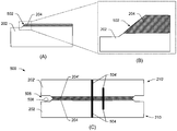
도 1의 (A)는 실시예에 따른, 다이의 상부 표면 상의 결함을 도시하는 측면도이다. 도 1의 (B)는 결함을 갖는 접합된 다이들의 단면을 도시하는 측면도이다. 도 1의 (C)는 결함을 갖지 않는 접합된 다이들의 단면을 도시하는 측면도이다.
도 2는 실시예에 따른, 적층 다이들을 처리하는 예시적인 공정을 예시하는 그래픽 흐름도이다.
도 3은 다른 실시예에 따른, 적층 다이들을 처리하는 예시적인 공정을 예시하는 그래픽 흐름도이다.
도 4는 추가 실시예에 따른, 적층 다이들을 처리하는 예시적인 공정을 예시하는 그래픽 흐름도이다.
도 5의 (A)는 실시예에 따른, 리세스된(recessed) 산화물 영역을 갖는 다이의 측면도이다. 도 5의 (B)는 리세스된 산화물 영역을 갖는 다이의 측면도의 확대도이다. 도 5의 (C)는 리세스된 산화물 영역을 갖는 접합된 다이 배열의 예이다.
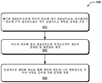
도 6은 실시예에 따른, 적층 다이들을 처리하기 위한 예시적인 공정을 예시하는 흐름도이다.
Claims (31)
- 마이크로 전자 시스템으로서,
적어도 베이스(base) 반도체 층 및 유전체 층으로 구성된 제1 마이크로 전자 컴포넌트 - 상기 유전체 층은 실질적으로 평탄한 표면을 가짐 -; 및
상기 제1 마이크로 전자 컴포넌트의 상기 유전체 층에 접착제 없이 직접 접합된 제2 마이크로 전자 컴포넌트 - 상기 유전체 층은 상기 유전체 층의 주연부(periphery)에서 언더컷(undercut)을 가져, 상기 유전체 층의 면적이 상기 제1 및/또는 제2 마이크로 전자 컴포넌트들의 풋프린트(footprint)의 면적보다 작음 - 를 포함하는, 마이크로 전자 시스템. - 제1항에 있어서, 상기 제1 마이크로 전자 컴포넌트의 상기 베이스 반도체 층은 상기 제1 마이크로 전자 컴포넌트의 상기 유전체 층의 상기 주연부에 있는 상기 언더컷에 대응하는 언더컷을 상기 베이스 반도체 층의 주연부에서 갖는, 마이크로 전자 시스템.
- 제1항에 있어서, 상기 제2 마이크로 전자 컴포넌트는 적어도 베이스 반도체 층 및 실질적으로 평탄한 표면을 갖는 유전체 층으로 구성되며, 상기 제1 마이크로 전자 컴포넌트의 상기 유전체 층은 상기 제2 마이크로 전자 컴포넌트의 상기 유전체 층에 직접 접합되고, 상기 제2 마이크로 전자 컴포넌트의 상기 유전체 층은 상기 제2 마이크로 전자 컴포넌트의 상기 유전체 층의 주연부에서 언더컷을 가져, 상기 제2 마이크로 전자 컴포넌트의 상기 유전체 층의 면적이 상기 제1 및/또는 제2 마이크로 전자 컴포넌트들의 상기 풋프린트의 상기 면적보다 작은, 마이크로 전자 시스템.
- 제3항에 있어서, 상기 제1 마이크로 전자 컴포넌트 및/또는 상기 제2 마이크로 전자 컴포넌트의 상기 베이스 반도체 층의 주연부에 있는 언더컷이 상기 제1 마이크로 전자 컴포넌트 및/또는 상기 제2 마이크로 전자 컴포넌트의 상기 유전체 층의 상기 주연부에 있는 언더컷에 대응하는, 마이크로 전자 시스템.
- 마이크로 전자 시스템으로서,
적어도 제1 베이스 반도체 층 및 제1 유전체 층으로 구성된 제1 마이크로 전자 컴포넌트 - 상기 제1 유전체 층은 제1 실질적으로 평탄한 표면을 가짐 -; 및
적어도 제2 베이스 반도체 층 및 제2 유전체 층으로 구성된 제2 마이크로 전자 컴포넌트 - 상기 제2 유전체 층은 제2 실질적으로 평탄한 표면을 갖고, 상기 제2 유전체 층은 상기 제1 및 제2 실질적으로 평탄한 표면들에서 상기 제1 유전체 층에 접착제 없이 직접 접합되고, 상기 제1 베이스 반도체 층 및 상기 제2 베이스 반도체 층은 각각 상기 제1 및 제2 베이스 반도체 층들의 주연부에서 언더컷을 가져, 상기 제1 베이스 반도체 층의 풋프린트의 면적 및 상기 제2 베이스 반도체 층의 풋프린트의 면적이 상기 제1 및/또는 제2 유전체 층들의 면적보다 작음 - 를 포함하는, 마이크로 전자 시스템. - 제5항에 있어서, 상기 언더컷은 상기 제1 마이크로 전자 컴포넌트 및/또는 상기 제2 마이크로 전자 컴포넌트의 상기 제1 및/또는 제2 유전체 층의 주연부에 있는 언더컷에 대응하는, 마이크로 전자 시스템.
- 마이크로 전자 시스템을 형성하기 위한 방법으로서,
웨이퍼 컴포넌트로부터 복수의 반도체 다이 컴포넌트들을 싱귤레이션(singulation)하는 단계 - 상기 반도체 다이 컴포넌트들은 각각 실질적으로 평탄한 표면을 가짐 -;
상기 복수의 반도체 다이 컴포넌트들의 에지들로부터 재료의 입자들 및 파편들을 제거하는 단계; 및
상기 실질적으로 평탄한 표면을 통해 상기 복수의 반도체 다이 컴포넌트들 중 하나 이상을 준비된 접합 표면에 접합하는 단계를 포함하는, 마이크로 전자 시스템을 형성하기 위한 방법. - 제7항에 있어서, 상기 복수의 반도체 다이 컴포넌트들의 상기 에지들로부터 상기 입자들 및 파편들을 제거하기 위해 상기 복수의 반도체 다이 컴포넌트들의 상기 에지들을 에칭하는 단계를 추가로 포함하는, 마이크로 전자 시스템을 형성하기 위한 방법.
- 제8항에 있어서, 상기 복수의 반도체 다이 컴포넌트들이 다이싱 캐리어(dicing carrier) 상에 있는 동안 상기 복수의 반도체 다이 컴포넌트들의 상기 에지들을 에칭하는 단계를 추가로 포함하는, 마이크로 전자 시스템을 형성하기 위한 방법.
- 제8항에 있어서, 플루오르화수소산 및 질산과 함께 벤조트라이아졸(BTA)을 포함하는 화학 에칭제를 사용하여 상기 복수의 반도체 다이 컴포넌트들의 상기 에지들을 에칭하는 단계를 추가로 포함하는, 마이크로 전자 시스템을 형성하기 위한 방법.
- 제8항에 있어서, 플라즈마 에칭을 사용하여 상기 복수의 반도체 다이 컴포넌트들의 상기 에지들을 에칭하는 단계를 추가로 포함하는, 마이크로 전자 시스템을 형성하기 위한 방법.
- 제8항에 있어서, 상기 복수의 반도체 다이 컴포넌트들 각각의 상기 에지들 중 하나 이상에 공간이 생성되도록 상기 복수의 반도체 다이 컴포넌트들의 두께를 감소시키기 위해 상기 복수의 반도체 다이 컴포넌트들의 상기 에지들을 에칭하는 단계를 추가로 포함하는, 마이크로 전자 시스템을 형성하기 위한 방법.
- 제8항에 있어서, 상기 반도체 다이 컴포넌트들은 상기 실질적으로 평탄한 표면으로서 산화물 층을 포함하고, 상기 에칭하는 단계는 상기 복수의 반도체 다이 컴포넌트들의 상기 에지들에서 상기 산화물 층의 적어도 일부를 제거하는 단계를 포함하는, 마이크로 전자 시스템을 형성하기 위한 방법.
- 제8항에 있어서, 에칭제로부터 상기 실질적으로 평탄한 표면을 보호하기 위해 상기 에칭하는 단계 전에 상기 복수의 반도체 다이 컴포넌트들의 상기 실질적으로 평탄한 표면에 보호 코팅을 적용하는 단계를 추가로 포함하는, 마이크로 전자 시스템을 형성하기 위한 방법.
- 제14항에 있어서,
상기 보호 코팅이 상기 복수의 반도체 다이 컴포넌트들의 주연부로부터 뒤로 물러나게 하기 위해 싱귤레이션하는 단계 후에 상기 복수의 반도체 다이 컴포넌트들을 가열하는 단계; 및
상기 복수의 반도체 다이 컴포넌트들의 상기 주연부를 사전 선택된 깊이까지 에칭하는 단계를 추가로 포함하는, 마이크로 전자 시스템을 형성하기 위한 방법. - 제15항에 있어서, 상기 복수의 반도체 다이 컴포넌트들은 베이스 반도체 층 위에 유전체 층을 포함하고, 상기 복수의 반도체 다이 컴포넌트들의 상기 주연부를 에칭하는 단계는 상기 유전체 층을 제거하고 상기 복수의 반도체 다이 컴포넌트들의 상기 주연부에서 상기 베이스 반도체 층을 노출시키는 단계를 포함하는, 마이크로 전자 시스템을 형성하기 위한 방법.
- 제7항에 있어서, 상기 복수의 반도체 다이 컴포넌트들의 상기 실질적으로 평탄한 표면을 에칭하는 단계를 추가로 포함하는, 마이크로 전자 시스템을 형성하기 위한 방법.
- 제17항에 있어서, 상기 실질적으로 평탄한 표면을 사전 선택된 깊이까지 또는 사전 선택된 지속 시간(duration) 동안 에칭하는 단계를 추가로 포함하는, 마이크로 전자 시스템을 형성하기 위한 방법.
- 제7항에 있어서, 상기 복수의 반도체 다이 컴포넌트들 중 상기 하나 이상은 접착제 없는 직접 접합 기술 또는 금속 대 금속 확산 접합(metal to metal diffusion bond)을 사용하여 접합되는, 마이크로 전자 시스템을 형성하기 위한 방법.
- 제7항에 있어서, 상기 방법은 상기 복수의 반도체 다이 컴포넌트들의 측벽으로부터 재료의 입자들 및 파편들을 제거하는 단계를 추가로 포함하며, 상기 입자들 및 파편들은 상기 복수의 반도체 다이 컴포넌트들의 상기 측벽을 에칭함으로써 상기 측벽으로부터 제거되는, 마이크로 전자 시스템을 형성하기 위한 방법.
- 제7항에 있어서, 상기 방법은 상기 복수의 반도체 다이 컴포넌트들의 측벽에 재료의 입자들 및 파편들을 코팅하는 단계를 추가로 포함하며, 상기 입자들 및 파편들은 상기 복수의 반도체 다이 컴포넌트들의 상기 측벽 상에 코팅 층을 침착(depositing)시킴으로써 상기 측벽에 코팅되는, 마이크로 전자 시스템을 형성하기 위한 방법.
- 제21항에 있어서, 유리, 붕소 도핑된 유리, 또는 인 도핑된 유리로 상기 복수의 반도체 다이 컴포넌트들의 상기 측벽을 스핀 코팅(spin coating) 또는 일렉트로 코팅(electrocoating)하는 단계를 추가로 포함하는, 마이크로 전자 시스템을 형성하기 위한 방법.
- 제22항에 있어서, 상기 유리, 상기 붕소 도핑된 유리, 또는 상기 인 도핑된 유리를 상기 복수의 반도체 다이 컴포넌트들의 상기 측벽에 열 경화시키는 단계를 추가로 포함하는, 마이크로 전자 시스템을 형성하기 위한 방법.
- 기기로서,
적어도 유전체 층으로 구성된 제1 마이크로 전자 컴포넌트 - 상기 유전체 층은 실질적으로 평탄한 표면을 가짐 -; 및
상기 제1 마이크로 전자 컴포넌트의 상기 유전체 층에 접착제 없이 직접 접합된 제2 마이크로 전자 컴포넌트 - 상기 유전체 층은 상기 제1 마이크로 전자 컴포넌트의 주연부에서 언더컷을 가져, 상기 유전체 층의 면적이 상기 제1 및/또는 제2 마이크로 전자 컴포넌트들의 풋프린트의 면적보다 작음 - 를 포함하는, 기기. - 제21항에 있어서, 상기 제1 마이크로 전자 컴포넌트 또는 상기 제2 마이크로 전자 컴포넌트는 직접 밴드 갭 또는 간접 밴드 갭 반도체를 포함하는, 기기.
- 기기로서,
적어도 평탄한 유전체 층으로 구성된 제1 컴포넌트;
상기 제1 컴포넌트의 상기 유전체 층에 접착제 없이 직접 접합된 제2 컴포넌트 - 상기 유전체 층은 상기 제1 컴포넌트의 주연부에서 언더컷을 가짐 - 를 포함하는, 기기. - 제26항에 있어서, 상기 제1 컴포넌트 또는 상기 제2 컴포넌트는 직접 밴드 갭 또는 간접 밴드 갭 반도체를 포함하는, 기기.
- 제26항에 있어서, 상기 제1 컴포넌트 또는 상기 제2 컴포넌트는 비-반도체 재료를 포함하는, 기기.
- 제26항에 있어서, 상기 제1 컴포넌트 및 상기 제2 컴포넌트는 마이크로 전자 다이를 포함하는, 기기.
- 기기를 형성하기 위한 방법으로서,
실질적으로 평탄한 표면을 갖는 마이크로 전자 컴포넌트를 복수의 서브-컴포넌트들로 싱귤레이션하는 단계;
상기 서브-컴포넌트들의 에지들로부터 재료의 입자들 및 파편들을 제거하는 단계; 및
상기 서브-컴포넌트들 중 하나 이상을 실질적으로 평탄한 표면을 갖는 준비된 접합 표면에 접합하는 단계를 포함하는, 기기를 형성하기 위한 방법. - 기기로서,
적어도 평탄한 유전체 층으로 구성된 제1 컴포넌트;
제2 컴포넌트 - 상기 제2 컴포넌트는 상기 제1 컴포넌트의 상기 유전체 층에 접착제 없이 직접 접합되어, 상기 유전체 층의 면적이 상기 제1 및/또는 제2 마이크로 전자 컴포넌트들의 풋프린트의 면적보다 작음 - 를 포함하는, 기기.
Applications Claiming Priority (5)
| Application Number | Priority Date | Filing Date | Title |
|---|---|---|---|
| US201762504834P | 2017-05-11 | 2017-05-11 | |
| US62/504,834 | 2017-05-11 | ||
| US15/960,179 US10879212B2 (en) | 2017-05-11 | 2018-04-23 | Processed stacked dies |
| US15/960,179 | 2018-04-23 | ||
| PCT/US2018/029094 WO2018208500A1 (en) | 2017-05-11 | 2018-04-24 | Processed stacked dies |
Publications (2)
| Publication Number | Publication Date |
|---|---|
| KR20190140967A true KR20190140967A (ko) | 2019-12-20 |
| KR102320674B1 KR102320674B1 (ko) | 2021-11-01 |
Family
ID=64097487
Family Applications (1)
| Application Number | Title | Priority Date | Filing Date |
|---|---|---|---|
| KR1020197033591A Active KR102320674B1 (ko) | 2017-05-11 | 2018-04-24 | 처리된 적층 다이들 |
Country Status (7)
| Country | Link |
|---|---|
| US (4) | US10879212B2 (ko) |
| EP (2) | EP3635775B1 (ko) |
| JP (3) | JP7129427B2 (ko) |
| KR (1) | KR102320674B1 (ko) |
| CN (2) | CN110574151B (ko) |
| TW (3) | TWI749220B (ko) |
| WO (1) | WO2018208500A1 (ko) |
Cited By (2)
| Publication number | Priority date | Publication date | Assignee | Title |
|---|---|---|---|---|
| KR20240171162A (ko) * | 2022-05-18 | 2024-12-06 | 꼼미사리아 아 레네르지 아토미끄 에뜨 옥스 에너지스 앨터네이티브즈 | 소스 기판에서 목적 기판으로 층을 전사하는 방법 |
| KR20240172227A (ko) * | 2022-05-18 | 2024-12-09 | 꼼미사리아 아 레네르지 아토미끄 에뜨 옥스 에너지스 앨터네이티브즈 | 소스 기판에서 목적 기판으로 층을 전사하는 방법 |
Families Citing this family (116)
| Publication number | Priority date | Publication date | Assignee | Title |
|---|---|---|---|---|
| US7109092B2 (en) | 2003-05-19 | 2006-09-19 | Ziptronix, Inc. | Method of room temperature covalent bonding |
| US7485968B2 (en) | 2005-08-11 | 2009-02-03 | Ziptronix, Inc. | 3D IC method and device |
| US8735219B2 (en) | 2012-08-30 | 2014-05-27 | Ziptronix, Inc. | Heterogeneous annealing method and device |
| US20150262902A1 (en) | 2014-03-12 | 2015-09-17 | Invensas Corporation | Integrated circuits protected by substrates with cavities, and methods of manufacture |
| US11069734B2 (en) | 2014-12-11 | 2021-07-20 | Invensas Corporation | Image sensor device |
| US9741620B2 (en) | 2015-06-24 | 2017-08-22 | Invensas Corporation | Structures and methods for reliable packages |
| US10886250B2 (en) | 2015-07-10 | 2021-01-05 | Invensas Corporation | Structures and methods for low temperature bonding using nanoparticles |
| US9953941B2 (en) | 2015-08-25 | 2018-04-24 | Invensas Bonding Technologies, Inc. | Conductive barrier direct hybrid bonding |
| US9852988B2 (en) | 2015-12-18 | 2017-12-26 | Invensas Bonding Technologies, Inc. | Increased contact alignment tolerance for direct bonding |
| US10446532B2 (en) | 2016-01-13 | 2019-10-15 | Invensas Bonding Technologies, Inc. | Systems and methods for efficient transfer of semiconductor elements |
| US10204893B2 (en) | 2016-05-19 | 2019-02-12 | Invensas Bonding Technologies, Inc. | Stacked dies and methods for forming bonded structures |
| US10446487B2 (en) | 2016-09-30 | 2019-10-15 | Invensas Bonding Technologies, Inc. | Interface structures and methods for forming same |
| US10580735B2 (en) | 2016-10-07 | 2020-03-03 | Xcelsis Corporation | Stacked IC structure with system level wiring on multiple sides of the IC die |
| US10607136B2 (en) | 2017-08-03 | 2020-03-31 | Xcelsis Corporation | Time borrowing between layers of a three dimensional chip stack |
| US10672663B2 (en) | 2016-10-07 | 2020-06-02 | Xcelsis Corporation | 3D chip sharing power circuit |
| TWI822659B (zh) | 2016-10-27 | 2023-11-21 | 美商艾德亞半導體科技有限責任公司 | 用於低溫接合的結構和方法 |
| US10002844B1 (en) | 2016-12-21 | 2018-06-19 | Invensas Bonding Technologies, Inc. | Bonded structures |
| US10796936B2 (en) | 2016-12-22 | 2020-10-06 | Invensas Bonding Technologies, Inc. | Die tray with channels |
| US20180182665A1 (en) | 2016-12-28 | 2018-06-28 | Invensas Bonding Technologies, Inc. | Processed Substrate |
| WO2018125673A2 (en) | 2016-12-28 | 2018-07-05 | Invensas Bonding Technologies, Inc | Processing stacked substrates |
| TWI837879B (zh) | 2016-12-29 | 2024-04-01 | 美商艾德亞半導體接合科技有限公司 | 具有整合式被動構件的接合結構 |
| JP7030825B2 (ja) | 2017-02-09 | 2022-03-07 | インヴェンサス ボンディング テクノロジーズ インコーポレイテッド | 接合構造物 |
| US10629577B2 (en) | 2017-03-16 | 2020-04-21 | Invensas Corporation | Direct-bonded LED arrays and applications |
| US10515913B2 (en) | 2017-03-17 | 2019-12-24 | Invensas Bonding Technologies, Inc. | Multi-metal contact structure |
| US10508030B2 (en) | 2017-03-21 | 2019-12-17 | Invensas Bonding Technologies, Inc. | Seal for microelectronic assembly |
| WO2018183739A1 (en) | 2017-03-31 | 2018-10-04 | Invensas Bonding Technologies, Inc. | Interface structures and methods for forming same |
| US10269756B2 (en) | 2017-04-21 | 2019-04-23 | Invensas Bonding Technologies, Inc. | Die processing |
| US10879212B2 (en) | 2017-05-11 | 2020-12-29 | Invensas Bonding Technologies, Inc. | Processed stacked dies |
| US10529634B2 (en) | 2017-05-11 | 2020-01-07 | Invensas Bonding Technologies, Inc. | Probe methodology for ultrafine pitch interconnects |
| US10446441B2 (en) | 2017-06-05 | 2019-10-15 | Invensas Corporation | Flat metal features for microelectronics applications |
| US10217720B2 (en) | 2017-06-15 | 2019-02-26 | Invensas Corporation | Multi-chip modules formed using wafer-level processing of a reconstitute wafer |
| US10840205B2 (en) | 2017-09-24 | 2020-11-17 | Invensas Bonding Technologies, Inc. | Chemical mechanical polishing for hybrid bonding |
| US11195748B2 (en) | 2017-09-27 | 2021-12-07 | Invensas Corporation | Interconnect structures and methods for forming same |
| US11031285B2 (en) | 2017-10-06 | 2021-06-08 | Invensas Bonding Technologies, Inc. | Diffusion barrier collar for interconnects |
| US10658313B2 (en) | 2017-12-11 | 2020-05-19 | Invensas Bonding Technologies, Inc. | Selective recess |
| US11011503B2 (en) | 2017-12-15 | 2021-05-18 | Invensas Bonding Technologies, Inc. | Direct-bonded optoelectronic interconnect for high-density integrated photonics |
| US10923408B2 (en) | 2017-12-22 | 2021-02-16 | Invensas Bonding Technologies, Inc. | Cavity packages |
| US11380597B2 (en) | 2017-12-22 | 2022-07-05 | Invensas Bonding Technologies, Inc. | Bonded structures |
| US10727219B2 (en) | 2018-02-15 | 2020-07-28 | Invensas Bonding Technologies, Inc. | Techniques for processing devices |
| US11169326B2 (en) | 2018-02-26 | 2021-11-09 | Invensas Bonding Technologies, Inc. | Integrated optical waveguides, direct-bonded waveguide interface joints, optical routing and interconnects |
| US11256004B2 (en) | 2018-03-20 | 2022-02-22 | Invensas Bonding Technologies, Inc. | Direct-bonded lamination for improved image clarity in optical devices |
| US10991804B2 (en) | 2018-03-29 | 2021-04-27 | Xcelsis Corporation | Transistor level interconnection methodologies utilizing 3D interconnects |
| US11056348B2 (en) | 2018-04-05 | 2021-07-06 | Invensas Bonding Technologies, Inc. | Bonding surfaces for microelectronics |
| US11244916B2 (en) | 2018-04-11 | 2022-02-08 | Invensas Bonding Technologies, Inc. | Low temperature bonded structures |
| US10790262B2 (en) | 2018-04-11 | 2020-09-29 | Invensas Bonding Technologies, Inc. | Low temperature bonded structures |
| US10964664B2 (en) | 2018-04-20 | 2021-03-30 | Invensas Bonding Technologies, Inc. | DBI to Si bonding for simplified handle wafer |
| US11004757B2 (en) | 2018-05-14 | 2021-05-11 | Invensas Bonding Technologies, Inc. | Bonded structures |
| US11276676B2 (en) | 2018-05-15 | 2022-03-15 | Invensas Bonding Technologies, Inc. | Stacked devices and methods of fabrication |
| US10923413B2 (en) | 2018-05-30 | 2021-02-16 | Xcelsis Corporation | Hard IP blocks with physically bidirectional passageways |
| US11171117B2 (en) | 2018-06-12 | 2021-11-09 | Invensas Bonding Technologies, Inc. | Interlayer connection of stacked microelectronic components |
| US11393779B2 (en) | 2018-06-13 | 2022-07-19 | Invensas Bonding Technologies, Inc. | Large metal pads over TSV |
| WO2019241417A1 (en) | 2018-06-13 | 2019-12-19 | Invensas Bonding Technologies, Inc. | Tsv as pad |
| US10910344B2 (en) | 2018-06-22 | 2021-02-02 | Xcelsis Corporation | Systems and methods for releveled bump planes for chiplets |
| US11664357B2 (en) | 2018-07-03 | 2023-05-30 | Adeia Semiconductor Bonding Technologies Inc. | Techniques for joining dissimilar materials in microelectronics |
| WO2020010265A1 (en) | 2018-07-06 | 2020-01-09 | Invensas Bonding Technologies, Inc. | Microelectronic assemblies |
| WO2020010136A1 (en) | 2018-07-06 | 2020-01-09 | Invensas Bonding Technologies, Inc. | Molded direct bonded and interconnected stack |
| US12406959B2 (en) | 2018-07-26 | 2025-09-02 | Adeia Semiconductor Bonding Technologies Inc. | Post CMP processing for hybrid bonding |
| US11515291B2 (en) | 2018-08-28 | 2022-11-29 | Adeia Semiconductor Inc. | Integrated voltage regulator and passive components |
| US11296044B2 (en) | 2018-08-29 | 2022-04-05 | Invensas Bonding Technologies, Inc. | Bond enhancement structure in microelectronics for trapping contaminants during direct-bonding processes |
| US11011494B2 (en) | 2018-08-31 | 2021-05-18 | Invensas Bonding Technologies, Inc. | Layer structures for making direct metal-to-metal bonds at low temperatures in microelectronics |
| US11158573B2 (en) | 2018-10-22 | 2021-10-26 | Invensas Bonding Technologies, Inc. | Interconnect structures |
| US11244920B2 (en) | 2018-12-18 | 2022-02-08 | Invensas Bonding Technologies, Inc. | Method and structures for low temperature device bonding |
| KR20210104742A (ko) | 2019-01-14 | 2021-08-25 | 인벤사스 본딩 테크놀로지스 인코포레이티드 | 접합 구조체 |
| US11387202B2 (en) | 2019-03-01 | 2022-07-12 | Invensas Llc | Nanowire bonding interconnect for fine-pitch microelectronics |
| US11901281B2 (en) | 2019-03-11 | 2024-02-13 | Adeia Semiconductor Bonding Technologies Inc. | Bonded structures with integrated passive component |
| US10854578B2 (en) | 2019-03-29 | 2020-12-01 | Invensas Corporation | Diffused bitline replacement in stacked wafer memory |
| US11205625B2 (en) | 2019-04-12 | 2021-12-21 | Invensas Bonding Technologies, Inc. | Wafer-level bonding of obstructive elements |
| US11610846B2 (en) | 2019-04-12 | 2023-03-21 | Adeia Semiconductor Bonding Technologies Inc. | Protective elements for bonded structures including an obstructive element |
| US11373963B2 (en) | 2019-04-12 | 2022-06-28 | Invensas Bonding Technologies, Inc. | Protective elements for bonded structures |
| US11355404B2 (en) | 2019-04-22 | 2022-06-07 | Invensas Bonding Technologies, Inc. | Mitigating surface damage of probe pads in preparation for direct bonding of a substrate |
| US11385278B2 (en) | 2019-05-23 | 2022-07-12 | Invensas Bonding Technologies, Inc. | Security circuitry for bonded structures |
| US12374641B2 (en) | 2019-06-12 | 2025-07-29 | Adeia Semiconductor Bonding Technologies Inc. | Sealed bonded structures and methods for forming the same |
| US11296053B2 (en) | 2019-06-26 | 2022-04-05 | Invensas Bonding Technologies, Inc. | Direct bonded stack structures for increased reliability and improved yield in microelectronics |
| US12080672B2 (en) | 2019-09-26 | 2024-09-03 | Adeia Semiconductor Bonding Technologies Inc. | Direct gang bonding methods including directly bonding first element to second element to form bonded structure without adhesive |
| US12113054B2 (en) | 2019-10-21 | 2024-10-08 | Adeia Semiconductor Technologies Llc | Non-volatile dynamic random access memory |
| US11862602B2 (en) | 2019-11-07 | 2024-01-02 | Adeia Semiconductor Technologies Llc | Scalable architecture for reduced cycles across SOC |
| US11762200B2 (en) | 2019-12-17 | 2023-09-19 | Adeia Semiconductor Bonding Technologies Inc. | Bonded optical devices |
| US20210183803A1 (en) * | 2019-12-17 | 2021-06-17 | Micron Technology, Inc. | Reconstructed wafer to wafer bonding using a permanent bond with laser release |
| US11876076B2 (en) | 2019-12-20 | 2024-01-16 | Adeia Semiconductor Technologies Llc | Apparatus for non-volatile random access memory stacks |
| US11721653B2 (en) | 2019-12-23 | 2023-08-08 | Adeia Semiconductor Bonding Technologies Inc. | Circuitry for electrical redundancy in bonded structures |
| CN121793755A (zh) | 2019-12-23 | 2026-04-03 | 隔热半导体粘合技术公司 | 用于接合结构的电冗余 |
| DE102020116340B4 (de) * | 2020-02-27 | 2025-01-16 | Taiwan Semiconductor Manufacturing Co., Ltd. | Gestapelter bildsensorvorrichtung und deren herstellungsverfahren |
| CN115943489A (zh) | 2020-03-19 | 2023-04-07 | 隔热半导体粘合技术公司 | 用于直接键合结构的尺寸补偿控制 |
| US11742314B2 (en) | 2020-03-31 | 2023-08-29 | Adeia Semiconductor Bonding Technologies Inc. | Reliable hybrid bonded apparatus |
| US11735523B2 (en) | 2020-05-19 | 2023-08-22 | Adeia Semiconductor Bonding Technologies Inc. | Laterally unconfined structure |
| US11631647B2 (en) | 2020-06-30 | 2023-04-18 | Adeia Semiconductor Bonding Technologies Inc. | Integrated device packages with integrated device die and dummy element |
| JP7453874B2 (ja) * | 2020-07-30 | 2024-03-21 | 芝浦メカトロニクス株式会社 | 基板処理方法、および基板処理装置 |
| CN111968944A (zh) * | 2020-08-24 | 2020-11-20 | 浙江集迈科微电子有限公司 | 一种射频模组超薄堆叠工艺 |
| US11728273B2 (en) | 2020-09-04 | 2023-08-15 | Adeia Semiconductor Bonding Technologies Inc. | Bonded structure with interconnect structure |
| US11764177B2 (en) | 2020-09-04 | 2023-09-19 | Adeia Semiconductor Bonding Technologies Inc. | Bonded structure with interconnect structure |
| US11264357B1 (en) | 2020-10-20 | 2022-03-01 | Invensas Corporation | Mixed exposure for large die |
| KR20230097121A (ko) | 2020-10-29 | 2023-06-30 | 아데이아 세미컨덕터 본딩 테크놀로지스 인코포레이티드 | 직접 접합 방법 및 구조체 |
| CN116635998A (zh) * | 2020-10-29 | 2023-08-22 | 美商艾德亚半导体接合科技有限公司 | 直接键合方法和结构 |
| WO2022147430A1 (en) | 2020-12-28 | 2022-07-07 | Invensas Bonding Technologies, Inc. | Structures with through-substrate vias and methods for forming the same |
| US12456662B2 (en) | 2020-12-28 | 2025-10-28 | Adeia Semiconductor Bonding Technologies Inc. | Structures with through-substrate vias and methods for forming the same |
| CN116848631A (zh) | 2020-12-30 | 2023-10-03 | 美商艾德亚半导体接合科技有限公司 | 具有导电特征的结构及其形成方法 |
| EP4315411A4 (en) * | 2021-03-31 | 2025-04-30 | Adeia Semiconductor Bonding Technologies Inc. | DIRECT BINDING METHODS AND STRUCTURES |
| US12525572B2 (en) | 2021-03-31 | 2026-01-13 | Adeia Semiconductor Bonding Technologies Inc. | Direct bonding and debonding of carrier |
| JP2024528964A (ja) | 2021-08-02 | 2024-08-01 | アデイア セミコンダクター ボンディング テクノロジーズ インコーポレイテッド | ボンデッド構造体用の保護半導体素子 |
| WO2023044308A1 (en) * | 2021-09-14 | 2023-03-23 | Adeia Semiconductor Bonding Technologies Inc. | Method of bonding thin substrates |
| CN115910809A (zh) * | 2021-09-22 | 2023-04-04 | 中国科学院微电子研究所 | 一种芯片至晶圆直接混合键合方法和三维堆叠集成器件 |
| CN115841954A (zh) * | 2021-09-22 | 2023-03-24 | 中国科学院微电子研究所 | 一种三维堆叠集成器件及其直接混合键合工艺 |
| KR20240059637A (ko) | 2021-09-24 | 2024-05-07 | 아데이아 세미컨덕터 본딩 테크놀로지스 인코포레이티드 | 능동 인터포저를 가진 결합 구조체 |
| US12604771B2 (en) | 2021-10-28 | 2026-04-14 | Adeia Semiconductor Bonding Technologies Inc. | Direct bonding methods and structures |
| US12563749B2 (en) | 2021-10-28 | 2026-02-24 | Adeia Semiconductor Bonding Technologies Inc | Stacked electronic devices |
| US12557615B2 (en) | 2021-12-13 | 2026-02-17 | Adeia Semiconductor Technologies Llc | Methods for bonding semiconductor elements |
| JP2025500315A (ja) | 2021-12-20 | 2025-01-09 | アデイア セミコンダクター ボンディング テクノロジーズ インコーポレイテッド | ダイパッケージの熱電冷却 |
| US12512425B2 (en) | 2022-04-25 | 2025-12-30 | Adeia Semiconductor Bonding Technologies Inc. | Expansion controlled structure for direct bonding and method of forming same |
| JP2025517291A (ja) | 2022-05-23 | 2025-06-05 | アデイア セミコンダクター ボンディング テクノロジーズ インコーポレイテッド | ボンデッド構造体のための試験用素子 |
| KR20250105390A (ko) * | 2022-10-27 | 2025-07-08 | 도쿄엘렉트론가부시키가이샤 | 옮겨 싣기 장치, 기판 처리 장치, 옮겨 싣기 방법 및 기판 처리 방법 |
| US20240222319A1 (en) * | 2022-12-28 | 2024-07-04 | Adeia Semiconductor Bonding Technologies Inc. | Debonding repair devices |
| US12506114B2 (en) | 2022-12-29 | 2025-12-23 | Adeia Semiconductor Bonding Technologies Inc. | Directly bonded metal structures having aluminum features and methods of preparing same |
| US12545010B2 (en) | 2022-12-29 | 2026-02-10 | Adeia Semiconductor Bonding Technologies Inc. | Directly bonded metal structures having oxide layers therein |
| US12341083B2 (en) | 2023-02-08 | 2025-06-24 | Adeia Semiconductor Bonding Technologies Inc. | Electronic device cooling structures bonded to semiconductor elements |
| US12598962B2 (en) | 2023-03-14 | 2026-04-07 | Adeia Semiconductor Bonding Technologies Inc. | System and method for bonding transparent conductor substrates |
| US12568780B2 (en) * | 2023-05-19 | 2026-03-03 | Taiwan Semiconductor Manufacturing Company, Ltd. | Semiconductor device and method of manufacturing |
Citations (7)
| Publication number | Priority date | Publication date | Assignee | Title |
|---|---|---|---|---|
| KR970072154A (ko) * | 1996-04-10 | 1997-11-07 | 윌리엄 비. 켐플러 | 부분 절단 후의 웨이퍼 세정 방법 |
| KR19990085633A (ko) * | 1998-05-20 | 1999-12-15 | 윤종용 | 초음파를 이용한 웨이퍼세척방법 |
| US20070123061A1 (en) * | 2005-11-25 | 2007-05-31 | Advanced Laser Separation International B.V. | Method of treating a substrate, method of processing a substrate using a laser beam, and arrangement |
| KR20090037784A (ko) * | 2007-10-12 | 2009-04-16 | 하마마츠 포토닉스 가부시키가이샤 | 가공 대상물 절단 방법 |
| KR20150005966A (ko) * | 2012-04-10 | 2015-01-15 | 어플라이드 머티어리얼스, 인코포레이티드 | 플라즈마 에칭을 갖는 하이브리드 멀티-스텝 레이저 스크라이빙 프로세스를 이용한 웨이퍼 다이싱 |
| KR20160037998A (ko) * | 2013-07-31 | 2016-04-06 | 어드밴스드 테크놀러지 머티리얼즈, 인코포레이티드 | Cu/W 호환성을 갖는, 금속 하드 마스크 및 에칭-후 잔여물을 제거하기 위한 수성 제형 |
| KR20160092900A (ko) * | 2015-01-28 | 2016-08-05 | 가부시끼가이샤 도시바 | 기판을 구비한 디바이스의 제조 방법 |
Family Cites Families (405)
| Publication number | Priority date | Publication date | Assignee | Title |
|---|---|---|---|---|
| JPH0272642A (ja) | 1988-09-07 | 1990-03-12 | Nec Corp | 基板の接続構造および接続方法 |
| JPH0344067A (ja) | 1989-07-11 | 1991-02-25 | Nec Corp | 半導体基板の積層方法 |
| US5019673A (en) | 1990-08-22 | 1991-05-28 | Motorola, Inc. | Flip-chip package for integrated circuits |
| JPH04337694A (ja) | 1991-05-15 | 1992-11-25 | Nec Yamagata Ltd | 電子部品保護用樹脂膜 |
| CA2083072C (en) | 1991-11-21 | 1998-02-03 | Shinichi Hasegawa | Method for manufacturing polyimide multilayer wiring substrate |
| US6008126A (en) | 1992-04-08 | 1999-12-28 | Elm Technology Corporation | Membrane dielectric isolation IC fabrication |
| US5341979A (en) | 1993-09-03 | 1994-08-30 | Motorola, Inc. | Method of bonding a semiconductor substrate to a support substrate and structure therefore |
| JPH07193294A (ja) | 1993-11-01 | 1995-07-28 | Matsushita Electric Ind Co Ltd | 電子部品およびその製造方法 |
| KR960009074A (ko) | 1994-08-29 | 1996-03-22 | 모리시다 요이치 | 반도체 장치 및 그 제조방법 |
| DE4433330C2 (de) | 1994-09-19 | 1997-01-30 | Fraunhofer Ges Forschung | Verfahren zur Herstellung von Halbleiterstrukturen mit vorteilhaften Hochfrequenzeigenschaften sowie eine Halbleiterwaferstruktur |
| JP3979687B2 (ja) | 1995-10-26 | 2007-09-19 | アプライド マテリアルズ インコーポレイテッド | ハロゲンをドープした酸化珪素膜の膜安定性を改良する方法 |
| KR100274333B1 (ko) | 1996-01-19 | 2001-01-15 | 모기 쥰이찌 | 도체층부착 이방성 도전시트 및 이를 사용한 배선기판 |
| US5956605A (en) | 1996-09-20 | 1999-09-21 | Micron Technology, Inc. | Use of nitrides for flip-chip encapsulation |
| US6221753B1 (en) | 1997-01-24 | 2001-04-24 | Micron Technology, Inc. | Flip chip technique for chip assembly |
| JP4032454B2 (ja) | 1997-06-27 | 2008-01-16 | ソニー株式会社 | 三次元回路素子の製造方法 |
| US6097096A (en) | 1997-07-11 | 2000-08-01 | Advanced Micro Devices | Metal attachment method and structure for attaching substrates at low temperatures |
| JP2000100679A (ja) | 1998-09-22 | 2000-04-07 | Canon Inc | 薄片化による基板間微小領域固相接合法及び素子構造 |
| JP3532788B2 (ja) | 1999-04-13 | 2004-05-31 | 唯知 須賀 | 半導体装置及びその製造方法 |
| JP2001102479A (ja) | 1999-09-27 | 2001-04-13 | Toshiba Corp | 半導体集積回路装置およびその製造方法 |
| US6984571B1 (en) | 1999-10-01 | 2006-01-10 | Ziptronix, Inc. | Three dimensional device integration method and integrated device |
| US6500694B1 (en) | 2000-03-22 | 2002-12-31 | Ziptronix, Inc. | Three dimensional device integration method and integrated device |
| US6902987B1 (en) | 2000-02-16 | 2005-06-07 | Ziptronix, Inc. | Method for low temperature bonding and bonded structure |
| JP2001313350A (ja) | 2000-04-28 | 2001-11-09 | Sony Corp | チップ状電子部品及びその製造方法、並びにその製造に用いる疑似ウエーハ及びその製造方法 |
| JP4322402B2 (ja) | 2000-06-22 | 2009-09-02 | 大日本印刷株式会社 | プリント配線基板及びその製造方法 |
| JP3440057B2 (ja) | 2000-07-05 | 2003-08-25 | 唯知 須賀 | 半導体装置およびその製造方法 |
| US6423640B1 (en) | 2000-08-09 | 2002-07-23 | Taiwan Semiconductor Manufacturing Co., Ltd. | Headless CMP process for oxide planarization |
| KR100386954B1 (ko) | 2000-11-17 | 2003-06-09 | 주영창 | 유리와 실리콘 기판의 저온 직접접합방법 |
| JP3420748B2 (ja) | 2000-12-14 | 2003-06-30 | 松下電器産業株式会社 | 半導体装置及びその製造方法 |
| JP2002353416A (ja) | 2001-05-25 | 2002-12-06 | Sony Corp | 半導体記憶装置およびその製造方法 |
| US6651866B2 (en) | 2001-10-17 | 2003-11-25 | Lilogix, Inc. | Precision bond head for mounting semiconductor chips |
| US6887769B2 (en) | 2002-02-06 | 2005-05-03 | Intel Corporation | Dielectric recess for wafer-to-wafer and die-to-die metal bonding and method of fabricating the same |
| TWI309074B (en) * | 2002-02-07 | 2009-04-21 | Advanced Epitaxy Technology | Method of forming semiconductor device |
| US6762076B2 (en) | 2002-02-20 | 2004-07-13 | Intel Corporation | Process of vertically stacking multiple wafers supporting different active integrated circuit (IC) devices |
| US7105980B2 (en) | 2002-07-03 | 2006-09-12 | Sawtek, Inc. | Saw filter device and method employing normal temperature bonding for producing desirable filter production and performance characteristics |
| JP4083502B2 (ja) | 2002-08-19 | 2008-04-30 | 株式会社フジミインコーポレーテッド | 研磨方法及びそれに用いられる研磨用組成物 |
| JP4579489B2 (ja) | 2002-09-02 | 2010-11-10 | 新光電気工業株式会社 | 半導体チップ製造方法及び半導体チップ |
| US7023093B2 (en) | 2002-10-24 | 2006-04-04 | International Business Machines Corporation | Very low effective dielectric constant interconnect Structures and methods for fabricating the same |
| JP2004193493A (ja) | 2002-12-13 | 2004-07-08 | Nec Machinery Corp | ダイピックアップ方法および装置 |
| US7354798B2 (en) | 2002-12-20 | 2008-04-08 | International Business Machines Corporation | Three-dimensional device fabrication method |
| TW586677U (en) | 2003-01-22 | 2004-05-01 | Via Tech Inc | Stack structure of chip package |
| US6962835B2 (en) | 2003-02-07 | 2005-11-08 | Ziptronix, Inc. | Method for room temperature metal direct bonding |
| TWI239629B (en) | 2003-03-17 | 2005-09-11 | Seiko Epson Corp | Method of manufacturing semiconductor device, semiconductor device, circuit substrate and electronic apparatus |
| US6908027B2 (en) | 2003-03-31 | 2005-06-21 | Intel Corporation | Complete device layer transfer without edge exclusion via direct wafer bonding and constrained bond-strengthening process |
| US7109092B2 (en) | 2003-05-19 | 2006-09-19 | Ziptronix, Inc. | Method of room temperature covalent bonding |
| TWI275168B (en) | 2003-06-06 | 2007-03-01 | Sanyo Electric Co | Semiconductor device and method for making the same |
| US20050026397A1 (en) | 2003-07-28 | 2005-02-03 | International Business Machines Corporation | Crack stop for low k dielectrics |
| US6873049B2 (en) | 2003-07-31 | 2005-03-29 | The Boeing Company | Near hermetic power chip on board device and manufacturing method therefor |
| US6867073B1 (en) | 2003-10-21 | 2005-03-15 | Ziptronix, Inc. | Single mask via method and device |
| US7205233B2 (en) * | 2003-11-07 | 2007-04-17 | Applied Materials, Inc. | Method for forming CoWRe alloys by electroless deposition |
| KR100538158B1 (ko) | 2004-01-09 | 2005-12-22 | 삼성전자주식회사 | 웨이퍼 레벨 적층 칩 접착 방법 |
| US20050161808A1 (en) * | 2004-01-22 | 2005-07-28 | Anderson Douglas G. | Wafer, intermediate wafer assembly and associated method for fabricating a silicon on insulator wafer having an improved edge profile |
| CN102290425B (zh) | 2004-08-20 | 2014-04-02 | Kamiyacho知识产权控股公司 | 具有三维层叠结构的半导体器件的制造方法 |
| US20060057945A1 (en) | 2004-09-16 | 2006-03-16 | Chia-Lin Hsu | Chemical mechanical polishing process |
| US7566634B2 (en) | 2004-09-24 | 2009-07-28 | Interuniversitair Microelektronica Centrum (Imec) | Method for chip singulation |
| US20060076634A1 (en) | 2004-09-27 | 2006-04-13 | Lauren Palmateer | Method and system for packaging MEMS devices with incorporated getter |
| US7262492B2 (en) | 2004-09-28 | 2007-08-28 | Intel Corporation | Semiconducting device that includes wirebonds |
| FR2880184B1 (fr) * | 2004-12-28 | 2007-03-30 | Commissariat Energie Atomique | Procede de detourage d'une structure obtenue par assemblage de deux plaques |
| GB0505680D0 (en) | 2005-03-22 | 2005-04-27 | Cambridge Display Tech Ltd | Apparatus and method for increased device lifetime in an organic electro-luminescent device |
| JP4275096B2 (ja) | 2005-04-14 | 2009-06-10 | パナソニック株式会社 | 半導体チップの製造方法 |
| US7354862B2 (en) | 2005-04-18 | 2008-04-08 | Intel Corporation | Thin passivation layer on 3D devices |
| JP4983049B2 (ja) | 2005-06-24 | 2012-07-25 | セイコーエプソン株式会社 | 半導体装置および電子機器 |
| US7485968B2 (en) | 2005-08-11 | 2009-02-03 | Ziptronix, Inc. | 3D IC method and device |
| US7193423B1 (en) | 2005-12-12 | 2007-03-20 | International Business Machines Corporation | Wafer-to-wafer alignments |
| US7781309B2 (en) | 2005-12-22 | 2010-08-24 | Sumco Corporation | Method for manufacturing direct bonded SOI wafer and direct bonded SOI wafer manufactured by the method |
| US20070158024A1 (en) | 2006-01-11 | 2007-07-12 | Symbol Technologies, Inc. | Methods and systems for removing multiple die(s) from a surface |
| TWI299552B (en) | 2006-03-24 | 2008-08-01 | Advanced Semiconductor Eng | Package structure |
| US7972683B2 (en) | 2006-03-28 | 2011-07-05 | Innovative Micro Technology | Wafer bonding material with embedded conductive particles |
| US7635650B2 (en) | 2006-04-14 | 2009-12-22 | Sony Corporation | Prevention of plasma induced damage arising from etching of crack stop trenches in multi-layered low-k semiconductor devices |
| JP2007305667A (ja) | 2006-05-09 | 2007-11-22 | Toshiba Corp | 半導体装置及びその製造方法 |
| US7385283B2 (en) | 2006-06-27 | 2008-06-10 | Taiwan Semiconductor Manufacturing Co., Ltd. | Three dimensional integrated circuit and method of making the same |
| US7750488B2 (en) | 2006-07-10 | 2010-07-06 | Tezzaron Semiconductor, Inc. | Method for bonding wafers to produce stacked integrated circuits |
| KR100809696B1 (ko) | 2006-08-08 | 2008-03-06 | 삼성전자주식회사 | 사이즈가 상이한 복수의 반도체 칩이 적층된 멀티 칩패키지 및 그 제조방법 |
| US7901989B2 (en) | 2006-10-10 | 2011-03-08 | Tessera, Inc. | Reconstituted wafer level stacking |
| JP5011981B2 (ja) | 2006-11-30 | 2012-08-29 | 富士通株式会社 | デバイス素子製造方法およびダイシング方法 |
| US8178964B2 (en) | 2007-03-30 | 2012-05-15 | Advanced Chip Engineering Technology, Inc. | Semiconductor device package with die receiving through-hole and dual build-up layers over both side-surfaces for WLP and method of the same |
| US8178963B2 (en) | 2007-01-03 | 2012-05-15 | Advanced Chip Engineering Technology Inc. | Wafer level package with die receiving through-hole and method of the same |
| US20080165521A1 (en) | 2007-01-09 | 2008-07-10 | Kerry Bernstein | Three-dimensional architecture for self-checking and self-repairing integrated circuits |
| US7803693B2 (en) | 2007-02-15 | 2010-09-28 | John Trezza | Bowed wafer hybridization compensation |
| JP2008258383A (ja) | 2007-04-04 | 2008-10-23 | Spansion Llc | 半導体装置及びその製造方法 |
| US8119500B2 (en) * | 2007-04-25 | 2012-02-21 | Taiwan Semiconductor Manufacturing Company, Ltd. | Wafer bonding |
| DE102007020656B4 (de) | 2007-04-30 | 2009-05-07 | Infineon Technologies Ag | Werkstück mit Halbleiterchips, Halbleiterbauteil und Verfahren zur Herstellung eines Werkstücks mit Halbleiterchips |
| US20090001599A1 (en) | 2007-06-28 | 2009-01-01 | Spansion Llc | Die attachment, die stacking, and wire embedding using film |
| US20090029274A1 (en) | 2007-07-25 | 2009-01-29 | 3M Innovative Properties Company | Method for removing contamination with fluorinated compositions |
| JP2009135348A (ja) | 2007-12-03 | 2009-06-18 | Panasonic Corp | 半導体チップと半導体装置およびそれらの製造方法 |
| CN105161429B (zh) | 2008-01-14 | 2018-06-05 | 加利福尼亚大学董事会 | 垂直除气通道 |
| US7871902B2 (en) | 2008-02-13 | 2011-01-18 | Infineon Technologies Ag | Crack stop trenches |
| EP2255378B1 (en) | 2008-03-05 | 2015-08-05 | The Board of Trustees of the University of Illinois | Stretchable and foldable electronic devices |
| CN102015943A (zh) | 2008-03-07 | 2011-04-13 | 3M创新有限公司 | 具有图案化背衬的切割带和晶粒附连粘合剂 |
| TWI515863B (zh) * | 2008-03-12 | 2016-01-01 | 英維瑟斯公司 | 載體安裝式電氣互連晶粒組成件 |
| KR20090106822A (ko) | 2008-04-07 | 2009-10-12 | 삼성전자주식회사 | 웨이퍼 본딩 방법 및 그 방법에 의해 본딩된 웨이퍼 구조체 |
| US8253230B2 (en) | 2008-05-15 | 2012-08-28 | Micron Technology, Inc. | Disabling electrical connections using pass-through 3D interconnects and associated systems and methods |
| US8349635B1 (en) | 2008-05-20 | 2013-01-08 | Silicon Laboratories Inc. | Encapsulated MEMS device and method to form the same |
| US8513810B2 (en) | 2008-07-31 | 2013-08-20 | Nec Corporation | Semiconductor device and method of manufacturing same |
| WO2010024678A1 (en) | 2008-09-01 | 2010-03-04 | Nederlandse Organisatie Voor Toegepast-Natuurwetenschappelijk Onderzoek Tno | Chip die clamping device and transfer method |
| US9893004B2 (en) | 2011-07-27 | 2018-02-13 | Broadpak Corporation | Semiconductor interposer integration |
| JP2010073964A (ja) | 2008-09-19 | 2010-04-02 | Fujitsu Microelectronics Ltd | 半導体装置の製造方法 |
| US7843052B1 (en) | 2008-11-13 | 2010-11-30 | Amkor Technology, Inc. | Semiconductor devices and fabrication methods thereof |
| WO2010057068A2 (en) | 2008-11-16 | 2010-05-20 | Suss Microtec, Inc. | Method and apparatus for wafer bonding with enhanced wafer mating |
| US8506867B2 (en) | 2008-11-19 | 2013-08-13 | Semprius, Inc. | Printing semiconductor elements by shear-assisted elastomeric stamp transfer |
| KR100945800B1 (ko) | 2008-12-09 | 2010-03-05 | 김영혜 | 이종 접합 웨이퍼 제조방법 |
| US8476165B2 (en) | 2009-04-01 | 2013-07-02 | Tokyo Electron Limited | Method for thinning a bonding wafer |
| JP2010245383A (ja) | 2009-04-08 | 2010-10-28 | Elpida Memory Inc | 半導体装置および半導体装置の製造方法 |
| JP5304536B2 (ja) | 2009-08-24 | 2013-10-02 | ソニー株式会社 | 半導体装置 |
| US8482132B2 (en) | 2009-10-08 | 2013-07-09 | International Business Machines Corporation | Pad bonding employing a self-aligned plated liner for adhesion enhancement |
| US9202769B2 (en) | 2009-11-25 | 2015-12-01 | Stats Chippac, Ltd. | Semiconductor device and method of forming thermal lid for balancing warpage and thermal management |
| EP2339614A1 (en) * | 2009-12-22 | 2011-06-29 | Imec | Method for stacking semiconductor chips |
| FR2954585B1 (fr) | 2009-12-23 | 2012-03-02 | Soitec Silicon Insulator Technologies | Procede de realisation d'une heterostructure avec minimisation de contrainte |
| US8138014B2 (en) | 2010-01-29 | 2012-03-20 | Stats Chippac, Ltd. | Method of forming thin profile WLCSP with vertical interconnect over package footprint |
| JP2011171614A (ja) | 2010-02-22 | 2011-09-01 | Casio Computer Co Ltd | 半導体装置及び半導体装置の製造方法 |
| US8901736B2 (en) | 2010-05-28 | 2014-12-02 | Taiwan Semiconductor Manufacturing Company, Ltd. | Strength of micro-bump joints |
| JP5123357B2 (ja) | 2010-06-17 | 2013-01-23 | 株式会社日立ハイテクインスツルメンツ | ダイボンダ及びピックアップ装置 |
| JP5517800B2 (ja) | 2010-07-09 | 2014-06-11 | キヤノン株式会社 | 固体撮像装置用の部材および固体撮像装置の製造方法 |
| US8481406B2 (en) | 2010-07-15 | 2013-07-09 | Soitec | Methods of forming bonded semiconductor structures |
| US8415808B2 (en) | 2010-07-28 | 2013-04-09 | Sandisk Technologies Inc. | Semiconductor device with die stack arrangement including staggered die and efficient wire bonding |
| US8361842B2 (en) | 2010-07-30 | 2013-01-29 | Taiwan Semiconductor Manufacturing Company, Ltd. | Embedded wafer-level bonding approaches |
| US8288201B2 (en) | 2010-08-25 | 2012-10-16 | Stats Chippac, Ltd. | Semiconductor device and method of forming FO-WLCSP with discrete semiconductor components mounted under and over semiconductor die |
| JP5183708B2 (ja) | 2010-09-21 | 2013-04-17 | 株式会社日立製作所 | 半導体装置およびその製造方法 |
| KR20120032254A (ko) | 2010-09-28 | 2012-04-05 | 삼성전자주식회사 | 반도체 적층 패키지 및 이의 제조 방법 |
| FR2966283B1 (fr) | 2010-10-14 | 2012-11-30 | Soi Tec Silicon On Insulator Tech Sa | Procede pour realiser une structure de collage |
| US8377798B2 (en) | 2010-11-10 | 2013-02-19 | Taiwan Semiconductor Manufacturing Co., Ltd | Method and structure for wafer to wafer bonding in semiconductor packaging |
| US8476146B2 (en) | 2010-12-03 | 2013-07-02 | Taiwan Semiconductor Manufacturing Company, Ltd. | Reducing wafer distortion through a low CTE layer |
| US8735260B2 (en) * | 2010-12-13 | 2014-05-27 | Taiwan Semiconductor Manufacturing Company, Ltd. | Method to prevent metal pad damage in wafer level package |
| US8620164B2 (en) | 2011-01-20 | 2013-12-31 | Intel Corporation | Hybrid III-V silicon laser formed by direct bonding |
| JP5659033B2 (ja) | 2011-02-04 | 2015-01-28 | 株式会社東芝 | 半導体装置の製造方法 |
| US8988299B2 (en) | 2011-02-17 | 2015-03-24 | International Business Machines Corporation | Integrated antenna for RFIC package applications |
| US8623702B2 (en) | 2011-02-24 | 2014-01-07 | Stats Chippac, Ltd. | Semiconductor device and method of forming conductive THV and RDL on opposite sides of semiconductor die for RDL-to-RDL bonding |
| WO2012125632A1 (en) * | 2011-03-16 | 2012-09-20 | Memc Electronic Materials, Inc. | Silicon on insulator structures having high resistivity regions in the handle wafer and methods for producing such structures |
| US8501537B2 (en) | 2011-03-31 | 2013-08-06 | Soitec | Methods for bonding semiconductor structures involving annealing processes, and bonded semiconductor structures formed using such methods |
| US8716105B2 (en) | 2011-03-31 | 2014-05-06 | Soitec | Methods for bonding semiconductor structures involving annealing processes, and bonded semiconductor structures and intermediate structures formed using such methods |
| KR20120123919A (ko) | 2011-05-02 | 2012-11-12 | 삼성전자주식회사 | 칩 적층 반도체 패키지 제조 방법 및 이에 의해 제조된 칩 적층 반도체 패키지 |
| KR101952976B1 (ko) | 2011-05-24 | 2019-02-27 | 소니 주식회사 | 반도체 장치 |
| US9029242B2 (en) | 2011-06-15 | 2015-05-12 | Applied Materials, Inc. | Damage isolation by shaped beam delivery in laser scribing process |
| US8728934B2 (en) | 2011-06-24 | 2014-05-20 | Tessera, Inc. | Systems and methods for producing flat surfaces in interconnect structures |
| JP5982748B2 (ja) | 2011-08-01 | 2016-08-31 | ソニー株式会社 | 半導体装置、半導体装置の製造方法、および電子機器 |
| US8896125B2 (en) | 2011-07-05 | 2014-11-25 | Sony Corporation | Semiconductor device, fabrication method for a semiconductor device and electronic apparatus |
| US8697493B2 (en) | 2011-07-18 | 2014-04-15 | Soitec | Bonding surfaces for direct bonding of semiconductor structures |
| US8710648B2 (en) | 2011-08-09 | 2014-04-29 | Alpha & Omega Semiconductor, Inc. | Wafer level packaging structure with large contact area and preparation method thereof |
| US8441131B2 (en) | 2011-09-12 | 2013-05-14 | Globalfoundries Inc. | Strain-compensating fill patterns for controlling semiconductor chip package interactions |
| KR101906408B1 (ko) | 2011-10-04 | 2018-10-11 | 삼성전자주식회사 | 반도체 패키지 및 그 제조 방법 |
| US9076664B2 (en) * | 2011-10-07 | 2015-07-07 | Freescale Semiconductor, Inc. | Stacked semiconductor die with continuous conductive vias |
| JP5780228B2 (ja) | 2011-11-11 | 2015-09-16 | 住友ベークライト株式会社 | 半導体装置の製造方法 |
| TWI467736B (zh) | 2012-01-04 | 2015-01-01 | 國立交通大學 | 立體積體電路裝置 |
| US8698308B2 (en) | 2012-01-31 | 2014-04-15 | Taiwan Semiconductor Manufacturing Company, Ltd. | Bump structural designs to minimize package defects |
| JP5994274B2 (ja) | 2012-02-14 | 2016-09-21 | ソニー株式会社 | 半導体装置、半導体装置の製造方法、及び、電子機器 |
| CN103377911B (zh) | 2012-04-16 | 2016-09-21 | 中国科学院微电子研究所 | 提高化学机械平坦化工艺均匀性的方法 |
| US9142517B2 (en) | 2012-06-05 | 2015-09-22 | Taiwan Semiconductor Manufacturing Company, Ltd. | Hybrid bonding mechanisms for semiconductor wafers |
| US8809123B2 (en) | 2012-06-05 | 2014-08-19 | Taiwan Semiconductor Manufacturing Company, Ltd. | Three dimensional integrated circuit structures and hybrid bonding methods for semiconductor wafers |
| DE102012105059A1 (de) * | 2012-06-12 | 2013-12-12 | Epcos Ag | Verfahren zur Herstellung eines Vielschichtbauelements und Vielschichtbauelement |
| US8723309B2 (en) | 2012-06-14 | 2014-05-13 | Stats Chippac Ltd. | Integrated circuit packaging system with through silicon via and method of manufacture thereof |
| FR2993400A1 (fr) | 2012-07-12 | 2014-01-17 | St Microelectronics Crolles 2 | Structure integree tridimensionnelle apte a detecter une elevation de temperature |
| US8759961B2 (en) | 2012-07-16 | 2014-06-24 | International Business Machines Corporation | Underfill material dispensing for stacked semiconductor chips |
| US8963336B2 (en) | 2012-08-03 | 2015-02-24 | Samsung Electronics Co., Ltd. | Semiconductor packages, methods of manufacturing the same, and semiconductor package structures including the same |
| US8735219B2 (en) | 2012-08-30 | 2014-05-27 | Ziptronix, Inc. | Heterogeneous annealing method and device |
| US20140070405A1 (en) | 2012-09-13 | 2014-03-13 | Globalfoundries Inc. | Stacked semiconductor devices with a glass window wafer having an engineered coefficient of thermal expansion and methods of making same |
| US9368404B2 (en) | 2012-09-28 | 2016-06-14 | Plasma-Therm Llc | Method for dicing a substrate with back metal |
| DE102012224310A1 (de) | 2012-12-21 | 2014-06-26 | Tesa Se | Gettermaterial enthaltendes Klebeband |
| US20140175655A1 (en) | 2012-12-22 | 2014-06-26 | Industrial Technology Research Institute | Chip bonding structure and manufacturing method thereof |
| TWI518991B (zh) | 2013-02-08 | 2016-01-21 | 巽晨國際股份有限公司 | Integrated antenna and integrated circuit components of the shielding module |
| US8946784B2 (en) | 2013-02-18 | 2015-02-03 | Taiwan Semiconductor Manufacturing Company, Ltd. | Method and apparatus for image sensor packaging |
| US9443796B2 (en) | 2013-03-15 | 2016-09-13 | Taiwan Semiconductor Manufacturing Company, Ltd. | Air trench in packages incorporating hybrid bonding |
| US8802538B1 (en) | 2013-03-15 | 2014-08-12 | Taiwan Semiconductor Manufacturing Company, Ltd. | Methods for hybrid wafer bonding |
| US9054063B2 (en) | 2013-04-05 | 2015-06-09 | Infineon Technologies Ag | High power single-die semiconductor package |
| WO2014176561A1 (en) | 2013-04-25 | 2014-10-30 | Skorpios Technologies, Inc. | Method and system for height registration during chip bonding |
| US9064937B2 (en) | 2013-05-30 | 2015-06-23 | International Business Machines Corporation | Substrate bonding with diffusion barrier structures |
| FR3007403B1 (fr) | 2013-06-20 | 2016-08-05 | Commissariat Energie Atomique | Procede de realisation d'un dispositif microelectronique mecaniquement autonome |
| KR102077153B1 (ko) | 2013-06-21 | 2020-02-14 | 삼성전자주식회사 | 관통전극을 갖는 반도체 패키지 및 그 제조방법 |
| JP2015012244A (ja) | 2013-07-01 | 2015-01-19 | 株式会社東芝 | 半導体発光素子 |
| US9929050B2 (en) | 2013-07-16 | 2018-03-27 | Taiwan Semiconductor Manufacturing Company, Ltd. | Mechanisms for forming three-dimensional integrated circuit (3DIC) stacking structure |
| US9324698B2 (en) | 2013-08-13 | 2016-04-26 | Taiwan Semiconductor Manufacturing Company, Ltd. | Multi-chip structure and method of forming same |
| WO2015040784A1 (ja) | 2013-09-17 | 2015-03-26 | パナソニックIpマネジメント株式会社 | 半導体装置及びその製造方法 |
| JP6212720B2 (ja) | 2013-09-20 | 2017-10-18 | パナソニックIpマネジメント株式会社 | 半導体装置及びその製造方法 |
| US9723716B2 (en) | 2013-09-27 | 2017-08-01 | Infineon Technologies Ag | Contact pad structure, an electronic component, and a method for manufacturing a contact pad structure |
| FR3011679B1 (fr) | 2013-10-03 | 2017-01-27 | Commissariat Energie Atomique | Procede ameliore d'assemblage par collage direct entre deux elements, chaque element comprenant des portions de metal et de materiaux dielectriques |
| KR102143518B1 (ko) | 2013-10-16 | 2020-08-11 | 삼성전자 주식회사 | 칩 적층 반도체 패키지 및 그 제조 방법 |
| US9257399B2 (en) | 2013-10-17 | 2016-02-09 | Taiwan Semiconductor Manufacturing Company, Ltd. | 3D integrated circuit and methods of forming the same |
| US9373527B2 (en) | 2013-10-30 | 2016-06-21 | Taiwan Semiconductor Manufacturing Company, Ltd. | Chip on package structure and method |
| US9530730B2 (en) | 2013-11-08 | 2016-12-27 | Taiwan Semiconductor Manufacturing Company, Ltd. | Configurable routing for packaging applications |
| JP6441025B2 (ja) | 2013-11-13 | 2018-12-19 | 株式会社東芝 | 半導体チップの製造方法 |
| US9570421B2 (en) | 2013-11-14 | 2017-02-14 | Taiwan Semiconductor Manufacturing Co., Ltd. | Stacking of multiple dies for forming three dimensional integrated circuit (3DIC) structure |
| US9330954B2 (en) * | 2013-11-22 | 2016-05-03 | Invensas Corporation | Substrate-to-carrier adhesion without mechanical adhesion between abutting surfaces thereof |
| JP2015115446A (ja) | 2013-12-11 | 2015-06-22 | 株式会社東芝 | 半導体装置の製造方法 |
| US9437572B2 (en) | 2013-12-18 | 2016-09-06 | Taiwan Semiconductor Manufacturing Company, Ltd. | Conductive pad structure for hybrid bonding and methods of forming same |
| US9768038B2 (en) | 2013-12-23 | 2017-09-19 | STATS ChipPAC, Pte. Ltd. | Semiconductor device and method of making embedded wafer level chip scale packages |
| US9653442B2 (en) | 2014-01-17 | 2017-05-16 | Taiwan Semiconductor Manufacturing Company, Ltd. | Integrated circuit package and methods of forming same |
| US9343433B2 (en) | 2014-01-28 | 2016-05-17 | Taiwan Semiconductor Manufacturing Company, Ltd. | Packages with stacked dies and methods of forming the same |
| US9293437B2 (en) | 2014-02-20 | 2016-03-22 | Taiwan Semiconductor Manufacturing Company, Ltd. | Functional block stacked 3DIC and method of making same |
| US20150255349A1 (en) | 2014-03-07 | 2015-09-10 | JAMES Matthew HOLDEN | Approaches for cleaning a wafer during hybrid laser scribing and plasma etching wafer dicing processes |
| US9355997B2 (en) | 2014-03-12 | 2016-05-31 | Invensas Corporation | Integrated circuit assemblies with reinforcement frames, and methods of manufacture |
| US20150262902A1 (en) | 2014-03-12 | 2015-09-17 | Invensas Corporation | Integrated circuits protected by substrates with cavities, and methods of manufacture |
| US9418924B2 (en) | 2014-03-20 | 2016-08-16 | Invensas Corporation | Stacked die integrated circuit |
| US9230941B2 (en) | 2014-03-28 | 2016-01-05 | Taiwan Semiconductor Manufacturing Company, Ltd. | Bonding structure for stacked semiconductor devices |
| US9299736B2 (en) | 2014-03-28 | 2016-03-29 | Taiwan Semiconductor Manufacturing Company, Ltd. | Hybrid bonding with uniform pattern density |
| US9076860B1 (en) * | 2014-04-04 | 2015-07-07 | Applied Materials, Inc. | Residue removal from singulated die sidewall |
| US8975163B1 (en) * | 2014-04-10 | 2015-03-10 | Applied Materials, Inc. | Laser-dominated laser scribing and plasma etch hybrid wafer dicing |
| US9601463B2 (en) | 2014-04-17 | 2017-03-21 | Taiwan Semiconductor Manufacturing Company, Ltd. | Fan-out stacked system in package (SIP) and the methods of making the same |
| US9472458B2 (en) | 2014-06-04 | 2016-10-18 | Semiconductor Components Industries, Llc | Method of reducing residual contamination in singulated semiconductor die |
| JP2016018879A (ja) | 2014-07-08 | 2016-02-01 | 株式会社東芝 | 半導体装置および半導体装置の製造方法 |
| KR102275705B1 (ko) | 2014-07-11 | 2021-07-09 | 삼성전자주식회사 | 웨이퍼 대 웨이퍼 접합 구조 |
| US9601437B2 (en) * | 2014-09-09 | 2017-03-21 | Nxp B.V. | Plasma etching and stealth dicing laser process |
| US10468381B2 (en) | 2014-09-29 | 2019-11-05 | Apple Inc. | Wafer level integration of passive devices |
| US9536848B2 (en) | 2014-10-16 | 2017-01-03 | Globalfoundries Inc. | Bond pad structure for low temperature flip chip bonding |
| US9673096B2 (en) * | 2014-11-14 | 2017-06-06 | Infineon Technologies Ag | Method for processing a semiconductor substrate and a method for processing a semiconductor wafer |
| US9394161B2 (en) | 2014-11-14 | 2016-07-19 | Taiwan Semiconductor Manufacturing Co., Ltd. | MEMS and CMOS integration with low-temperature bonding |
| US9899442B2 (en) | 2014-12-11 | 2018-02-20 | Invensas Corporation | Image sensor device |
| US11069734B2 (en) | 2014-12-11 | 2021-07-20 | Invensas Corporation | Image sensor device |
| US10319701B2 (en) | 2015-01-07 | 2019-06-11 | Taiwan Semiconductor Manufacturing Company, Ltd. | Bonded 3D integrated circuit (3DIC) structure |
| US9508660B2 (en) | 2015-02-10 | 2016-11-29 | Intel Corporation | Microelectronic die having chamfered corners |
| DE102015103274A1 (de) | 2015-03-06 | 2016-09-08 | HARTING Electronics GmbH | Kabelabdichtung |
| JP6738591B2 (ja) | 2015-03-13 | 2020-08-12 | 古河電気工業株式会社 | 半導体ウェハの処理方法、半導体チップおよび表面保護テープ |
| US10068862B2 (en) | 2015-04-09 | 2018-09-04 | STATS ChipPAC Pte. Ltd. | Semiconductor device and method of forming a package in-fan out package |
| KR101664411B1 (ko) | 2015-06-04 | 2016-10-14 | 주식회사 에스에프에이반도체 | 웨이퍼 레벨의 팬 아웃 패키지 제조방법 |
| US9741620B2 (en) | 2015-06-24 | 2017-08-22 | Invensas Corporation | Structures and methods for reliable packages |
| US9704827B2 (en) | 2015-06-25 | 2017-07-11 | Taiwan Semiconductor Manufacturing Co., Ltd. | Hybrid bond pad structure |
| US9656852B2 (en) | 2015-07-06 | 2017-05-23 | Taiwan Semiconductor Manufacturing Company Ltd. | CMOS-MEMS device structure, bonding mesa structure and associated method |
| US10886250B2 (en) | 2015-07-10 | 2021-01-05 | Invensas Corporation | Structures and methods for low temperature bonding using nanoparticles |
| US10352991B2 (en) | 2015-07-21 | 2019-07-16 | Fermi Research Alliance, Llc | Edgeless large area ASIC |
| US10075657B2 (en) | 2015-07-21 | 2018-09-11 | Fermi Research Alliance, Llc | Edgeless large area camera system |
| US9728521B2 (en) | 2015-07-23 | 2017-08-08 | Taiwan Semiconductor Manufacturing Co., Ltd. | Hybrid bond using a copper alloy for yield improvement |
| US9559081B1 (en) | 2015-08-21 | 2017-01-31 | Apple Inc. | Independent 3D stacking |
| US9953941B2 (en) | 2015-08-25 | 2018-04-24 | Invensas Bonding Technologies, Inc. | Conductive barrier direct hybrid bonding |
| US9754891B2 (en) | 2015-09-23 | 2017-09-05 | International Business Machines Corporation | Low-temperature diffusion doping of copper interconnects independent of seed layer composition |
| WO2017052652A1 (en) | 2015-09-25 | 2017-03-30 | Intel Corporation | Combination of semiconductor die with another die by hybrid bonding |
| US10032751B2 (en) | 2015-09-28 | 2018-07-24 | Invensas Corporation | Ultrathin layer for forming a capacitive interface between joined integrated circuit components |
| US9524959B1 (en) | 2015-11-04 | 2016-12-20 | Taiwan Semiconductor Manufacturing Company, Ltd. | System on integrated chips and methods of forming same |
| US9666560B1 (en) | 2015-11-25 | 2017-05-30 | Invensas Corporation | Multi-chip microelectronic assembly with built-up fine-patterned circuit structure |
| JP2017098452A (ja) * | 2015-11-26 | 2017-06-01 | 株式会社ディスコ | 洗浄方法 |
| US9496239B1 (en) | 2015-12-11 | 2016-11-15 | International Business Machines Corporation | Nitride-enriched oxide-to-oxide 3D wafer bonding |
| US9852988B2 (en) | 2015-12-18 | 2017-12-26 | Invensas Bonding Technologies, Inc. | Increased contact alignment tolerance for direct bonding |
| US9881882B2 (en) | 2016-01-06 | 2018-01-30 | Mediatek Inc. | Semiconductor package with three-dimensional antenna |
| US20170200659A1 (en) | 2016-01-08 | 2017-07-13 | International Business Machines Corporation | Porous underfill enabling rework |
| US9923011B2 (en) * | 2016-01-12 | 2018-03-20 | Taiwan Semiconductor Manufacturing Co., Ltd. | Semiconductor device structure with stacked semiconductor dies |
| US10446532B2 (en) | 2016-01-13 | 2019-10-15 | Invensas Bonding Technologies, Inc. | Systems and methods for efficient transfer of semiconductor elements |
| JP2017130610A (ja) | 2016-01-22 | 2017-07-27 | ソニー株式会社 | イメージセンサ、製造方法、及び、電子機器 |
| JP2019511834A (ja) | 2016-02-16 | 2019-04-25 | ジーレイ スイッツァーランド エスアー | 接合インターフェースを横断する電荷輸送のための構造、システムおよび方法 |
| US10636767B2 (en) | 2016-02-29 | 2020-04-28 | Invensas Corporation | Correction die for wafer/die stack |
| US11373990B2 (en) * | 2016-02-29 | 2022-06-28 | Semtech Corporation | Semiconductor device and method of stacking semiconductor die for system-level ESD protection |
| EP3437133A4 (en) | 2016-04-01 | 2019-11-27 | INTEL Corporation | TECHNIQUES FOR STACKING MATRICES AND ASSOCIATED CONFIGURATIONS |
| US10026716B2 (en) | 2016-04-15 | 2018-07-17 | Taiwan Semiconductor Manufacturing Company, Ltd. | 3DIC formation with dies bonded to formed RDLs |
| US10204893B2 (en) | 2016-05-19 | 2019-02-12 | Invensas Bonding Technologies, Inc. | Stacked dies and methods for forming bonded structures |
| KR102505856B1 (ko) | 2016-06-09 | 2023-03-03 | 삼성전자 주식회사 | 웨이퍼 대 웨이퍼 접합 구조체 |
| KR102521881B1 (ko) | 2016-06-15 | 2023-04-18 | 삼성전자주식회사 | 반도체 소자 및 이의 제조 방법 |
| US9818729B1 (en) | 2016-06-16 | 2017-11-14 | Taiwan Semiconductor Manufacturing Company, Ltd. | Package-on-package structure and method |
| US10163675B2 (en) | 2016-06-24 | 2018-12-25 | Invensas Corporation | Method and apparatus for stacking devices in an integrated circuit assembly |
| US9859254B1 (en) | 2016-06-30 | 2018-01-02 | Taiwan Semiconductor Manufacturing Company Ltd. | Semiconductor structure and a manufacturing method thereof |
| US9941241B2 (en) | 2016-06-30 | 2018-04-10 | International Business Machines Corporation | Method for wafer-wafer bonding |
| KR102570582B1 (ko) | 2016-06-30 | 2023-08-24 | 삼성전자 주식회사 | 반도체 패키지 및 그 제조 방법 |
| US9966360B2 (en) | 2016-07-05 | 2018-05-08 | Taiwan Semiconductor Manufacturing Co., Ltd. | Semiconductor package and manufacturing method thereof |
| US9892961B1 (en) | 2016-08-09 | 2018-02-13 | International Business Machines Corporation | Air gap spacer formation for nano-scale semiconductor devices |
| US10672741B2 (en) | 2016-08-18 | 2020-06-02 | Taiwan Semiconductor Manufacturing Company, Ltd. | Semiconductor packages with thermal-electrical-mechanical chips and methods of forming the same |
| KR102649471B1 (ko) | 2016-09-05 | 2024-03-21 | 삼성전자주식회사 | 반도체 패키지 및 그의 제조 방법 |
| US9768133B1 (en) | 2016-09-22 | 2017-09-19 | Taiwan Semiconductor Manufacturing Company, Ltd. | Semiconductor package and method of forming the same |
| US10446487B2 (en) | 2016-09-30 | 2019-10-15 | Invensas Bonding Technologies, Inc. | Interface structures and methods for forming same |
| US10580735B2 (en) | 2016-10-07 | 2020-03-03 | Xcelsis Corporation | Stacked IC structure with system level wiring on multiple sides of the IC die |
| US10607136B2 (en) | 2017-08-03 | 2020-03-31 | Xcelsis Corporation | Time borrowing between layers of a three dimensional chip stack |
| US10672663B2 (en) | 2016-10-07 | 2020-06-02 | Xcelsis Corporation | 3D chip sharing power circuit |
| US9722098B1 (en) | 2016-10-18 | 2017-08-01 | Ase Electronics (M) Sdn Bhd | Semiconductor device package and method of manufacturing the same |
| US10304801B2 (en) | 2016-10-31 | 2019-05-28 | Taiwan Semiconductor Manufacturing Company, Ltd. | Redistribution layers in semiconductor packages and methods of forming same |
| US20180130768A1 (en) | 2016-11-09 | 2018-05-10 | Unisem (M) Berhad | Substrate Based Fan-Out Wafer Level Packaging |
| US10163750B2 (en) | 2016-12-05 | 2018-12-25 | Taiwan Semiconductor Manufacturing Company, Ltd. | Package structure for heat dissipation |
| US10453832B2 (en) | 2016-12-15 | 2019-10-22 | Taiwan Semiconductor Manufacturing Co., Ltd. | Seal ring structures and methods of forming same |
| US10002844B1 (en) | 2016-12-21 | 2018-06-19 | Invensas Bonding Technologies, Inc. | Bonded structures |
| WO2018125673A2 (en) | 2016-12-28 | 2018-07-05 | Invensas Bonding Technologies, Inc | Processing stacked substrates |
| US20180182665A1 (en) | 2016-12-28 | 2018-06-28 | Invensas Bonding Technologies, Inc. | Processed Substrate |
| TWI837879B (zh) | 2016-12-29 | 2024-04-01 | 美商艾德亞半導體接合科技有限公司 | 具有整合式被動構件的接合結構 |
| US20180190583A1 (en) | 2016-12-29 | 2018-07-05 | Invensas Bonding Technologies, Inc. | Bonded structures with integrated passive component |
| US10276909B2 (en) | 2016-12-30 | 2019-04-30 | Invensas Bonding Technologies, Inc. | Structure comprising at least a first element bonded to a carrier having a closed metallic channel waveguide formed therein |
| US10431614B2 (en) | 2017-02-01 | 2019-10-01 | Semiconductor Components Industries, Llc | Edge seals for semiconductor packages |
| US9865567B1 (en) | 2017-02-02 | 2018-01-09 | Xilinx, Inc. | Heterogeneous integration of integrated circuit device and companion device |
| JP7030825B2 (ja) | 2017-02-09 | 2022-03-07 | インヴェンサス ボンディング テクノロジーズ インコーポレイテッド | 接合構造物 |
| US10629577B2 (en) | 2017-03-16 | 2020-04-21 | Invensas Corporation | Direct-bonded LED arrays and applications |
| US10515913B2 (en) | 2017-03-17 | 2019-12-24 | Invensas Bonding Technologies, Inc. | Multi-metal contact structure |
| US10508030B2 (en) | 2017-03-21 | 2019-12-17 | Invensas Bonding Technologies, Inc. | Seal for microelectronic assembly |
| JP6640780B2 (ja) | 2017-03-22 | 2020-02-05 | キオクシア株式会社 | 半導体装置の製造方法および半導体装置 |
| WO2018183739A1 (en) | 2017-03-31 | 2018-10-04 | Invensas Bonding Technologies, Inc. | Interface structures and methods for forming same |
| US10269756B2 (en) | 2017-04-21 | 2019-04-23 | Invensas Bonding Technologies, Inc. | Die processing |
| US10580823B2 (en) | 2017-05-03 | 2020-03-03 | United Microelectronics Corp. | Wafer level packaging method |
| US10879212B2 (en) | 2017-05-11 | 2020-12-29 | Invensas Bonding Technologies, Inc. | Processed stacked dies |
| US10446441B2 (en) | 2017-06-05 | 2019-10-15 | Invensas Corporation | Flat metal features for microelectronics applications |
| US10217720B2 (en) | 2017-06-15 | 2019-02-26 | Invensas Corporation | Multi-chip modules formed using wafer-level processing of a reconstitute wafer |
| US10658335B2 (en) | 2017-06-16 | 2020-05-19 | Futurewei Technologies, Inc. | Heterogenous 3D chip stack for a mobile processor |
| US10707145B2 (en) | 2017-09-08 | 2020-07-07 | Kemet Electronics Corporation | High density multi-component packages |
| US10840205B2 (en) | 2017-09-24 | 2020-11-17 | Invensas Bonding Technologies, Inc. | Chemical mechanical polishing for hybrid bonding |
| US11195748B2 (en) | 2017-09-27 | 2021-12-07 | Invensas Corporation | Interconnect structures and methods for forming same |
| US10332899B2 (en) | 2017-09-29 | 2019-06-25 | Intel Corporation | 3D package having edge-aligned die stack with direct inter-die wire connections |
| US11031285B2 (en) | 2017-10-06 | 2021-06-08 | Invensas Bonding Technologies, Inc. | Diffusion barrier collar for interconnects |
| US11251157B2 (en) | 2017-11-01 | 2022-02-15 | Taiwan Semiconductor Manufacturing Company, Ltd. | Die stack structure with hybrid bonding structure and method of fabricating the same and package |
| US10685935B2 (en) | 2017-11-15 | 2020-06-16 | Taiwan Semiconductor Manufacturing Company, Ltd. | Forming metal bonds with recesses |
| US10364144B2 (en) | 2017-11-17 | 2019-07-30 | Texas Instruments Incorporated | Hermetically sealed package for mm-wave molecular spectroscopy cell |
| US10672820B2 (en) | 2017-11-23 | 2020-06-02 | Taiwan Semiconductor Manufacturing Co., Ltd. | Hybrid bonded structure |
| US11011503B2 (en) | 2017-12-15 | 2021-05-18 | Invensas Bonding Technologies, Inc. | Direct-bonded optoelectronic interconnect for high-density integrated photonics |
| US10923408B2 (en) | 2017-12-22 | 2021-02-16 | Invensas Bonding Technologies, Inc. | Cavity packages |
| US11380597B2 (en) | 2017-12-22 | 2022-07-05 | Invensas Bonding Technologies, Inc. | Bonded structures |
| US11127738B2 (en) | 2018-02-09 | 2021-09-21 | Xcelsis Corporation | Back biasing of FD-SOI circuit blocks |
| US10727219B2 (en) | 2018-02-15 | 2020-07-28 | Invensas Bonding Technologies, Inc. | Techniques for processing devices |
| US11169326B2 (en) | 2018-02-26 | 2021-11-09 | Invensas Bonding Technologies, Inc. | Integrated optical waveguides, direct-bonded waveguide interface joints, optical routing and interconnects |
| US11256004B2 (en) | 2018-03-20 | 2022-02-22 | Invensas Bonding Technologies, Inc. | Direct-bonded lamination for improved image clarity in optical devices |
| US10991804B2 (en) | 2018-03-29 | 2021-04-27 | Xcelsis Corporation | Transistor level interconnection methodologies utilizing 3D interconnects |
| US11056348B2 (en) | 2018-04-05 | 2021-07-06 | Invensas Bonding Technologies, Inc. | Bonding surfaces for microelectronics |
| US10790262B2 (en) | 2018-04-11 | 2020-09-29 | Invensas Bonding Technologies, Inc. | Low temperature bonded structures |
| US10964664B2 (en) | 2018-04-20 | 2021-03-30 | Invensas Bonding Technologies, Inc. | DBI to Si bonding for simplified handle wafer |
| US10937743B2 (en) | 2018-04-30 | 2021-03-02 | Taiwan Semiconductor Manufacturing Company, Ltd. | Mixing organic materials into hybrid packages |
| US11398258B2 (en) | 2018-04-30 | 2022-07-26 | Invensas Llc | Multi-die module with low power operation |
| US10403577B1 (en) | 2018-05-03 | 2019-09-03 | Invensas Corporation | Dielets on flexible and stretchable packaging for microelectronics |
| US11469138B2 (en) | 2018-05-04 | 2022-10-11 | Taiwan Semiconductor Manufacturing Company, Ltd. | Via for coupling attached component upper electrode to substrate |
| US11004757B2 (en) | 2018-05-14 | 2021-05-11 | Invensas Bonding Technologies, Inc. | Bonded structures |
| US11276676B2 (en) | 2018-05-15 | 2022-03-15 | Invensas Bonding Technologies, Inc. | Stacked devices and methods of fabrication |
| US10510629B2 (en) | 2018-05-18 | 2019-12-17 | Taiwan Semiconductor Manufacturing Company, Ltd. | Integrated circuit package and method of forming same |
| US10727204B2 (en) | 2018-05-29 | 2020-07-28 | Advances Micro Devices, Inc. | Die stacking for multi-tier 3D integration |
| US10923413B2 (en) | 2018-05-30 | 2021-02-16 | Xcelsis Corporation | Hard IP blocks with physically bidirectional passageways |
| US11171117B2 (en) | 2018-06-12 | 2021-11-09 | Invensas Bonding Technologies, Inc. | Interlayer connection of stacked microelectronic components |
| WO2019241417A1 (en) | 2018-06-13 | 2019-12-19 | Invensas Bonding Technologies, Inc. | Tsv as pad |
| US11393779B2 (en) | 2018-06-13 | 2022-07-19 | Invensas Bonding Technologies, Inc. | Large metal pads over TSV |
| US10910344B2 (en) | 2018-06-22 | 2021-02-02 | Xcelsis Corporation | Systems and methods for releveled bump planes for chiplets |
| US10333623B1 (en) | 2018-06-25 | 2019-06-25 | Taiwan Semiconductor Manufacturing Co., Ltd. | Optical transceiver |
| US11664357B2 (en) | 2018-07-03 | 2023-05-30 | Adeia Semiconductor Bonding Technologies Inc. | Techniques for joining dissimilar materials in microelectronics |
| WO2020010265A1 (en) | 2018-07-06 | 2020-01-09 | Invensas Bonding Technologies, Inc. | Microelectronic assemblies |
| WO2020010136A1 (en) | 2018-07-06 | 2020-01-09 | Invensas Bonding Technologies, Inc. | Molded direct bonded and interconnected stack |
| US12406959B2 (en) | 2018-07-26 | 2025-09-02 | Adeia Semiconductor Bonding Technologies Inc. | Post CMP processing for hybrid bonding |
| US10727205B2 (en) | 2018-08-15 | 2020-07-28 | Taiwan Semiconductor Manufacturing Co., Ltd. | Hybrid bonding technology for stacking integrated circuits |
| US11515291B2 (en) | 2018-08-28 | 2022-11-29 | Adeia Semiconductor Inc. | Integrated voltage regulator and passive components |
| US11296044B2 (en) | 2018-08-29 | 2022-04-05 | Invensas Bonding Technologies, Inc. | Bond enhancement structure in microelectronics for trapping contaminants during direct-bonding processes |
| US11011494B2 (en) | 2018-08-31 | 2021-05-18 | Invensas Bonding Technologies, Inc. | Layer structures for making direct metal-to-metal bonds at low temperatures in microelectronics |
| US10797031B2 (en) | 2018-09-20 | 2020-10-06 | Taiwan Semiconductor Manufacturing Company, Ltd. | Semiconductor package |
| US10868353B2 (en) | 2018-09-27 | 2020-12-15 | Taiwan Semiconductor Manufacturing Company, Ltd. | Electronic device and manufacturing method thereof |
| US11158573B2 (en) | 2018-10-22 | 2021-10-26 | Invensas Bonding Technologies, Inc. | Interconnect structures |
| US11158607B2 (en) | 2018-11-29 | 2021-10-26 | Apple Inc. | Wafer reconstitution and die-stitching |
| US11244920B2 (en) | 2018-12-18 | 2022-02-08 | Invensas Bonding Technologies, Inc. | Method and structures for low temperature device bonding |
| KR20210104742A (ko) | 2019-01-14 | 2021-08-25 | 인벤사스 본딩 테크놀로지스 인코포레이티드 | 접합 구조체 |
| US11387202B2 (en) | 2019-03-01 | 2022-07-12 | Invensas Llc | Nanowire bonding interconnect for fine-pitch microelectronics |
| US11901281B2 (en) | 2019-03-11 | 2024-02-13 | Adeia Semiconductor Bonding Technologies Inc. | Bonded structures with integrated passive component |
| US10770430B1 (en) | 2019-03-22 | 2020-09-08 | Xilinx, Inc. | Package integration for memory devices |
| US10854578B2 (en) | 2019-03-29 | 2020-12-01 | Invensas Corporation | Diffused bitline replacement in stacked wafer memory |
| US11373963B2 (en) | 2019-04-12 | 2022-06-28 | Invensas Bonding Technologies, Inc. | Protective elements for bonded structures |
| US11610846B2 (en) | 2019-04-12 | 2023-03-21 | Adeia Semiconductor Bonding Technologies Inc. | Protective elements for bonded structures including an obstructive element |
| US11205625B2 (en) | 2019-04-12 | 2021-12-21 | Invensas Bonding Technologies, Inc. | Wafer-level bonding of obstructive elements |
| US11355404B2 (en) | 2019-04-22 | 2022-06-07 | Invensas Bonding Technologies, Inc. | Mitigating surface damage of probe pads in preparation for direct bonding of a substrate |
| US11385278B2 (en) | 2019-05-23 | 2022-07-12 | Invensas Bonding Technologies, Inc. | Security circuitry for bonded structures |
| US12374641B2 (en) | 2019-06-12 | 2025-07-29 | Adeia Semiconductor Bonding Technologies Inc. | Sealed bonded structures and methods for forming the same |
| US11145623B2 (en) | 2019-06-14 | 2021-10-12 | Taiwan Semiconductor Manufacturing Company, Ltd. | Integrated circuit packages and methods of forming the same |
| US11296053B2 (en) | 2019-06-26 | 2022-04-05 | Invensas Bonding Technologies, Inc. | Direct bonded stack structures for increased reliability and improved yield in microelectronics |
| US11094613B2 (en) | 2019-08-22 | 2021-08-17 | Taiwan Semiconductor Manufacturing Company, Ltd. | Semiconductor structure and manufacturing method thereof |
| US12080672B2 (en) | 2019-09-26 | 2024-09-03 | Adeia Semiconductor Bonding Technologies Inc. | Direct gang bonding methods including directly bonding first element to second element to form bonded structure without adhesive |
| US12113054B2 (en) | 2019-10-21 | 2024-10-08 | Adeia Semiconductor Technologies Llc | Non-volatile dynamic random access memory |
| US11862602B2 (en) | 2019-11-07 | 2024-01-02 | Adeia Semiconductor Technologies Llc | Scalable architecture for reduced cycles across SOC |
| US11762200B2 (en) | 2019-12-17 | 2023-09-19 | Adeia Semiconductor Bonding Technologies Inc. | Bonded optical devices |
| US11876076B2 (en) | 2019-12-20 | 2024-01-16 | Adeia Semiconductor Technologies Llc | Apparatus for non-volatile random access memory stacks |
| US11721653B2 (en) | 2019-12-23 | 2023-08-08 | Adeia Semiconductor Bonding Technologies Inc. | Circuitry for electrical redundancy in bonded structures |
| CN121793755A (zh) | 2019-12-23 | 2026-04-03 | 隔热半导体粘合技术公司 | 用于接合结构的电冗余 |
| US20210242152A1 (en) | 2020-02-05 | 2021-08-05 | Invensas Bonding Technologies, Inc. | Selective alteration of interconnect pads for direct bonding |
| CN115943489A (zh) | 2020-03-19 | 2023-04-07 | 隔热半导体粘合技术公司 | 用于直接键合结构的尺寸补偿控制 |
| US11742314B2 (en) | 2020-03-31 | 2023-08-29 | Adeia Semiconductor Bonding Technologies Inc. | Reliable hybrid bonded apparatus |
| US11735523B2 (en) | 2020-05-19 | 2023-08-22 | Adeia Semiconductor Bonding Technologies Inc. | Laterally unconfined structure |
| US11631647B2 (en) | 2020-06-30 | 2023-04-18 | Adeia Semiconductor Bonding Technologies Inc. | Integrated device packages with integrated device die and dummy element |
| US11764177B2 (en) | 2020-09-04 | 2023-09-19 | Adeia Semiconductor Bonding Technologies Inc. | Bonded structure with interconnect structure |
| US11728273B2 (en) | 2020-09-04 | 2023-08-15 | Adeia Semiconductor Bonding Technologies Inc. | Bonded structure with interconnect structure |
| US11264357B1 (en) | 2020-10-20 | 2022-03-01 | Invensas Corporation | Mixed exposure for large die |
| CN116635998A (zh) | 2020-10-29 | 2023-08-22 | 美商艾德亚半导体接合科技有限公司 | 直接键合方法和结构 |
| KR20230097121A (ko) | 2020-10-29 | 2023-06-30 | 아데이아 세미컨덕터 본딩 테크놀로지스 인코포레이티드 | 직접 접합 방법 및 구조체 |
| US12456662B2 (en) | 2020-12-28 | 2025-10-28 | Adeia Semiconductor Bonding Technologies Inc. | Structures with through-substrate vias and methods for forming the same |
| WO2022147430A1 (en) | 2020-12-28 | 2022-07-07 | Invensas Bonding Technologies, Inc. | Structures with through-substrate vias and methods for forming the same |
| US20220208723A1 (en) | 2020-12-30 | 2022-06-30 | Invensas Bonding Technologies, Inc. | Directly bonded structures |
| CN116848631A (zh) | 2020-12-30 | 2023-10-03 | 美商艾德亚半导体接合科技有限公司 | 具有导电特征的结构及其形成方法 |
| KR20230153446A (ko) | 2021-03-03 | 2023-11-06 | 아데이아 세미컨덕터 본딩 테크놀로지스 인코포레이티드 | 직접 결합을 위한 접촉 구조 |
| US12525572B2 (en) | 2021-03-31 | 2026-01-13 | Adeia Semiconductor Bonding Technologies Inc. | Direct bonding and debonding of carrier |
| EP4315411A4 (en) | 2021-03-31 | 2025-04-30 | Adeia Semiconductor Bonding Technologies Inc. | DIRECT BINDING METHODS AND STRUCTURES |
| JP2024515032A (ja) | 2021-03-31 | 2024-04-04 | アデイア セミコンダクター ボンディング テクノロジーズ インコーポレイテッド | 担体の直接接合及び剥離 |
| KR20240028356A (ko) | 2021-06-30 | 2024-03-05 | 아데이아 세미컨덕터 본딩 테크놀로지스 인코포레이티드 | 결합층에서 라우팅 구조체를 갖는 소자 |
| KR20240036032A (ko) | 2021-07-16 | 2024-03-19 | 아데이아 세미컨덕터 본딩 테크놀로지스 인코포레이티드 | 접합된 구조물의 광학적 차단 보호 요소 |
| JP2024528964A (ja) | 2021-08-02 | 2024-08-01 | アデイア セミコンダクター ボンディング テクノロジーズ インコーポレイテッド | ボンデッド構造体用の保護半導体素子 |
| JP2024532903A (ja) | 2021-09-01 | 2024-09-10 | アデイア セミコンダクター テクノロジーズ リミテッド ライアビリティ カンパニー | インターポーザを備えた積層構造 |
| US20230067677A1 (en) | 2021-09-01 | 2023-03-02 | Invensas Bonding Technologies, Inc. | Sequences and equipment for direct bonding |
| WO2023044308A1 (en) | 2021-09-14 | 2023-03-23 | Adeia Semiconductor Bonding Technologies Inc. | Method of bonding thin substrates |
| KR20240059637A (ko) | 2021-09-24 | 2024-05-07 | 아데이아 세미컨덕터 본딩 테크놀로지스 인코포레이티드 | 능동 인터포저를 가진 결합 구조체 |
| JP2024538179A (ja) | 2021-10-18 | 2024-10-18 | アデイア セミコンダクター テクノロジーズ リミテッド ライアビリティ カンパニー | 結合構造における寄生容量の低減 |
| KR20240090512A (ko) | 2021-10-19 | 2024-06-21 | 아데이아 세미컨덕터 본딩 테크놀로지스 인코포레이티드 | 멀티-다이 스태킹에서의 적층된 인덕터 |
| EP4420197A4 (en) | 2021-10-22 | 2025-09-10 | Adeia Semiconductor Tech Llc | RADIO FREQUENCY DEVICE HOUSINGS |
| JP2024541923A (ja) | 2021-10-25 | 2024-11-13 | アデイア セミコンダクター ボンディング テクノロジーズ インコーポレイテッド | 積層化電子デバイス用の電力分配 |
| US20230125395A1 (en) | 2021-10-27 | 2023-04-27 | Adeia Semiconductor Bonding Technologies Inc. | Stacked structures with capacitive coupling connections |
| EP4423806A4 (en) | 2021-10-28 | 2025-09-24 | Adeia Semiconductor Bonding Technologies Inc | DIFFUSION BARRIERS AND ASSOCIATED FORMATION METHOD |
| US12604771B2 (en) | 2021-10-28 | 2026-04-14 | Adeia Semiconductor Bonding Technologies Inc. | Direct bonding methods and structures |
| US12563749B2 (en) | 2021-10-28 | 2026-02-24 | Adeia Semiconductor Bonding Technologies Inc | Stacked electronic devices |
| JP2024537478A (ja) | 2021-11-05 | 2024-10-10 | アデイア セミコンダクター ボンディング テクノロジーズ インコーポレイテッド | マルチチャンネル型デバイス積層化 |
| US20230154816A1 (en) | 2021-11-17 | 2023-05-18 | Adeia Semiconductor Bonding Technologies Inc. | Thermal bypass for stacked dies |
| US20230154828A1 (en) | 2021-11-18 | 2023-05-18 | Adeia Semiconductor Bonding Technologies Inc. | Fluid cooling for die stacks |
| US12557615B2 (en) | 2021-12-13 | 2026-02-17 | Adeia Semiconductor Technologies Llc | Methods for bonding semiconductor elements |
| WO2023114726A1 (en) | 2021-12-13 | 2023-06-22 | Adeia Semiconductor Bonding Technologies Inc. | Interconnect structures |
| US20230197453A1 (en) | 2021-12-17 | 2023-06-22 | Adeia Semiconductor Bonding Technologies Inc. | Structure with conductive feature for direct bonding and method of forming same |
| JP2025500315A (ja) | 2021-12-20 | 2025-01-09 | アデイア セミコンダクター ボンディング テクノロジーズ インコーポレイテッド | ダイパッケージの熱電冷却 |
| WO2023122510A1 (en) | 2021-12-20 | 2023-06-29 | Adeia Semiconductor Bonding Technologies Inc. | Thermoelectric cooling in microelectronics |
| EP4454005A4 (en) | 2021-12-20 | 2026-05-06 | Adeia Semiconductor Bonding Technologies Inc | Direct bonding and debonding of elements |
| JP2024545315A (ja) | 2021-12-22 | 2024-12-05 | アデイア セミコンダクター ボンディング テクノロジーズ インコーポレイテッド | 低応力直接ハイブリッド接合 |
| EP4454008A4 (en) | 2021-12-23 | 2025-11-05 | Adeia Semiconductor Bonding Technologies Inc | DIRECT CONNECTION TO ENCLOSURE SUBSTRATES |
| EP4454013A4 (en) | 2021-12-23 | 2025-07-30 | Adeia Semiconductor Bonding Technologies Inc | LINKED STRUCTURES COMPRISING INTERCONNECTING ASSEMBLIES |
| CN118613905A (zh) | 2021-12-23 | 2024-09-06 | 美商艾德亚半导体接合科技有限公司 | 用于管芯键合控制的装置和方法 |
| US20230207402A1 (en) | 2021-12-27 | 2023-06-29 | Adeia Semiconductor Bonding Technologies Inc. | Directly bonded frame wafers |
| WO2023147502A1 (en) | 2022-01-31 | 2023-08-03 | Adeia Semiconductor Bonding Technologies Inc. | Heat dissipating system for electronic devices |
| KR20240156613A (ko) | 2022-02-24 | 2024-10-30 | 아데이아 세미컨덕터 본딩 테크놀로지스 인코포레이티드 | 결합 구조체 |
| US20230299029A1 (en) | 2022-03-16 | 2023-09-21 | Adeia Semiconductor Bonding Technologies Inc. | Expansion control for bonding |
| US12512425B2 (en) | 2022-04-25 | 2025-12-30 | Adeia Semiconductor Bonding Technologies Inc. | Expansion controlled structure for direct bonding and method of forming same |
| US20230360950A1 (en) | 2022-05-05 | 2023-11-09 | Adeia Semiconductor Bonding Technologies Inc. | Gang-flipping of dies prior to bonding |
| WO2023215598A1 (en) | 2022-05-05 | 2023-11-09 | Adeia Semiconductor Bonding Technologies Inc. | Low temperature direct bonding |
| US20230369136A1 (en) | 2022-05-13 | 2023-11-16 | Adeia Semiconductor Bonding Technologies Inc. | Bonding surface validation on dicing tape |
| JP2025517291A (ja) | 2022-05-23 | 2025-06-05 | アデイア セミコンダクター ボンディング テクノロジーズ インコーポレイテッド | ボンデッド構造体のための試験用素子 |
| US20240038702A1 (en) | 2022-07-27 | 2024-02-01 | Adeia Semiconductor Bonding Technologies Inc. | High-performance hybrid bonded interconnect systems |
| WO2024054799A1 (en) | 2022-09-07 | 2024-03-14 | Adeia Semiconductor Bonding Technologies Inc. | Rapid thermal processing for direct bonding |
-
2018
- 2018-04-23 US US15/960,179 patent/US10879212B2/en active Active
- 2018-04-24 WO PCT/US2018/029094 patent/WO2018208500A1/en not_active Ceased
- 2018-04-24 JP JP2019562412A patent/JP7129427B2/ja active Active
- 2018-04-24 KR KR1020197033591A patent/KR102320674B1/ko active Active
- 2018-04-24 CN CN201880028854.7A patent/CN110574151B/zh active Active
- 2018-04-24 CN CN202311589853.9A patent/CN117497456A/zh active Pending
- 2018-04-24 EP EP18799043.7A patent/EP3635775B1/en active Active
- 2018-04-24 EP EP25163657.7A patent/EP4550400A3/en active Pending
- 2018-04-27 TW TW107114594A patent/TWI749220B/zh active
- 2018-04-27 TW TW110144066A patent/TWI809576B/zh active
- 2018-04-27 TW TW112122430A patent/TWI864826B/zh active
-
2020
- 2020-12-16 US US17/124,306 patent/US11652083B2/en active Active
-
2022
- 2022-08-22 JP JP2022131656A patent/JP2022163235A/ja active Pending
- 2022-12-29 US US18/148,369 patent/US12068278B2/en active Active
-
2024
- 2024-07-24 US US18/783,239 patent/US20240404990A1/en active Pending
- 2024-12-25 JP JP2024228795A patent/JP2025060841A/ja active Pending
Patent Citations (7)
| Publication number | Priority date | Publication date | Assignee | Title |
|---|---|---|---|---|
| KR970072154A (ko) * | 1996-04-10 | 1997-11-07 | 윌리엄 비. 켐플러 | 부분 절단 후의 웨이퍼 세정 방법 |
| KR19990085633A (ko) * | 1998-05-20 | 1999-12-15 | 윤종용 | 초음파를 이용한 웨이퍼세척방법 |
| US20070123061A1 (en) * | 2005-11-25 | 2007-05-31 | Advanced Laser Separation International B.V. | Method of treating a substrate, method of processing a substrate using a laser beam, and arrangement |
| KR20090037784A (ko) * | 2007-10-12 | 2009-04-16 | 하마마츠 포토닉스 가부시키가이샤 | 가공 대상물 절단 방법 |
| KR20150005966A (ko) * | 2012-04-10 | 2015-01-15 | 어플라이드 머티어리얼스, 인코포레이티드 | 플라즈마 에칭을 갖는 하이브리드 멀티-스텝 레이저 스크라이빙 프로세스를 이용한 웨이퍼 다이싱 |
| KR20160037998A (ko) * | 2013-07-31 | 2016-04-06 | 어드밴스드 테크놀러지 머티리얼즈, 인코포레이티드 | Cu/W 호환성을 갖는, 금속 하드 마스크 및 에칭-후 잔여물을 제거하기 위한 수성 제형 |
| KR20160092900A (ko) * | 2015-01-28 | 2016-08-05 | 가부시끼가이샤 도시바 | 기판을 구비한 디바이스의 제조 방법 |
Cited By (2)
| Publication number | Priority date | Publication date | Assignee | Title |
|---|---|---|---|---|
| KR20240171162A (ko) * | 2022-05-18 | 2024-12-06 | 꼼미사리아 아 레네르지 아토미끄 에뜨 옥스 에너지스 앨터네이티브즈 | 소스 기판에서 목적 기판으로 층을 전사하는 방법 |
| KR20240172227A (ko) * | 2022-05-18 | 2024-12-09 | 꼼미사리아 아 레네르지 아토미끄 에뜨 옥스 에너지스 앨터네이티브즈 | 소스 기판에서 목적 기판으로 층을 전사하는 방법 |
Also Published As
| Publication number | Publication date |
|---|---|
| JP2025060841A (ja) | 2025-04-10 |
| CN117497456A (zh) | 2024-02-02 |
| TW201907505A (zh) | 2019-02-16 |
| US20230282610A1 (en) | 2023-09-07 |
| US12068278B2 (en) | 2024-08-20 |
| US20180331066A1 (en) | 2018-11-15 |
| EP4550400A3 (en) | 2025-08-13 |
| JP2022163235A (ja) | 2022-10-25 |
| EP4550400A2 (en) | 2025-05-07 |
| CN110574151B (zh) | 2023-12-15 |
| TW202510203A (zh) | 2025-03-01 |
| US20240404990A1 (en) | 2024-12-05 |
| TW202209560A (zh) | 2022-03-01 |
| CN110574151A (zh) | 2019-12-13 |
| TWI749220B (zh) | 2021-12-11 |
| US10879212B2 (en) | 2020-12-29 |
| TWI864826B (zh) | 2024-12-01 |
| TWI809576B (zh) | 2023-07-21 |
| WO2018208500A1 (en) | 2018-11-15 |
| US11652083B2 (en) | 2023-05-16 |
| TW202343668A (zh) | 2023-11-01 |
| EP3635775A1 (en) | 2020-04-15 |
| EP3635775B1 (en) | 2025-03-19 |
| JP2020520118A (ja) | 2020-07-02 |
| KR102320674B1 (ko) | 2021-11-01 |
| EP3635775A4 (en) | 2021-05-26 |
| US20210104487A1 (en) | 2021-04-08 |
| JP7129427B2 (ja) | 2022-09-01 |
Similar Documents
| Publication | Publication Date | Title |
|---|---|---|
| US12068278B2 (en) | Processed stacked dies | |
| US12374556B2 (en) | Processing stacked substrates | |
| CN113410133B (zh) | 用于处理器件的技术 | |
| CN111834296A (zh) | 半导体器件和方法 | |
| US20080044985A1 (en) | Methods for releasably attaching sacrificial support members to microfeature workpieces and microfeature devices formed using such methods | |
| JP6062254B2 (ja) | ウエーハの加工方法 | |
| TWI916040B (zh) | 經處理的堆疊晶粒 | |
| US20250014912A1 (en) | Method for protecting active layers of electronic chips |
Legal Events
| Date | Code | Title | Description |
|---|---|---|---|
| PA0105 | International application |
St.27 status event code: A-0-1-A10-A15-nap-PA0105 |
|
| PG1501 | Laying open of application |
St.27 status event code: A-1-1-Q10-Q12-nap-PG1501 |
|
| A201 | Request for examination | ||
| A302 | Request for accelerated examination | ||
| E13-X000 | Pre-grant limitation requested |
St.27 status event code: A-2-3-E10-E13-lim-X000 |
|
| P11-X000 | Amendment of application requested |
St.27 status event code: A-2-2-P10-P11-nap-X000 |
|
| P13-X000 | Application amended |
St.27 status event code: A-2-2-P10-P13-nap-X000 |
|
| PA0201 | Request for examination |
St.27 status event code: A-1-2-D10-D11-exm-PA0201 |
|
| PA0302 | Request for accelerated examination |
St.27 status event code: A-1-2-D10-D17-exm-PA0302 St.27 status event code: A-1-2-D10-D16-exm-PA0302 |
|
| E902 | Notification of reason for refusal | ||
| PE0902 | Notice of grounds for rejection |
St.27 status event code: A-1-2-D10-D21-exm-PE0902 |
|
| E13-X000 | Pre-grant limitation requested |
St.27 status event code: A-2-3-E10-E13-lim-X000 |
|
| P11-X000 | Amendment of application requested |
St.27 status event code: A-2-2-P10-P11-nap-X000 |
|
| P13-X000 | Application amended |
St.27 status event code: A-2-2-P10-P13-nap-X000 |
|
| E701 | Decision to grant or registration of patent right | ||
| PE0701 | Decision of registration |
St.27 status event code: A-1-2-D10-D22-exm-PE0701 |
|
| GRNT | Written decision to grant | ||
| PR0701 | Registration of establishment |
St.27 status event code: A-2-4-F10-F11-exm-PR0701 |
|
| PR1002 | Payment of registration fee |
St.27 status event code: A-2-2-U10-U12-oth-PR1002 Fee payment year number: 1 |
|
| PG1601 | Publication of registration |
St.27 status event code: A-4-4-Q10-Q13-nap-PG1601 |
|
| PN2301 | Change of applicant |
St.27 status event code: A-5-5-R10-R13-asn-PN2301 St.27 status event code: A-5-5-R10-R11-asn-PN2301 |
|
| PR1001 | Payment of annual fee |
St.27 status event code: A-4-4-U10-U11-oth-PR1001 Fee payment year number: 4 |
|
| P22-X000 | Classification modified |
St.27 status event code: A-4-4-P10-P22-nap-X000 |