KR20200091490A - 대전 입자 다중-빔릿 장치 - Google Patents
대전 입자 다중-빔릿 장치 Download PDFInfo
- Publication number
- KR20200091490A KR20200091490A KR1020207020901A KR20207020901A KR20200091490A KR 20200091490 A KR20200091490 A KR 20200091490A KR 1020207020901 A KR1020207020901 A KR 1020207020901A KR 20207020901 A KR20207020901 A KR 20207020901A KR 20200091490 A KR20200091490 A KR 20200091490A
- Authority
- KR
- South Korea
- Prior art keywords
- electrodes
- charged particle
- manipulator device
- opening
- openings
- Prior art date
- Legal status (The legal status is an assumption and is not a legal conclusion. Google has not performed a legal analysis and makes no representation as to the accuracy of the status listed.)
- Granted
Links
Images




Classifications
-
- H—ELECTRICITY
- H01—ELECTRIC ELEMENTS
- H01J—ELECTRIC DISCHARGE TUBES OR DISCHARGE LAMPS
- H01J37/00—Discharge tubes with provision for introducing objects or material to be exposed to the discharge, e.g. for the purpose of examination or processing thereof
- H01J37/30—Electron-beam or ion-beam tubes for localised treatment of objects
- H01J37/3002—Details
- H01J37/3007—Electron or ion-optical systems
-
- H—ELECTRICITY
- H01—ELECTRIC ELEMENTS
- H01J—ELECTRIC DISCHARGE TUBES OR DISCHARGE LAMPS
- H01J37/00—Discharge tubes with provision for introducing objects or material to be exposed to the discharge, e.g. for the purpose of examination or processing thereof
- H01J37/30—Electron-beam or ion-beam tubes for localised treatment of objects
- H01J37/317—Electron-beam or ion-beam tubes for localised treatment of objects for changing properties of the objects or for applying thin layers thereon, e.g. for ion implantation
- H01J37/3174—Particle-beam lithography, e.g. electron beam lithography
-
- H—ELECTRICITY
- H01—ELECTRIC ELEMENTS
- H01J—ELECTRIC DISCHARGE TUBES OR DISCHARGE LAMPS
- H01J37/00—Discharge tubes with provision for introducing objects or material to be exposed to the discharge, e.g. for the purpose of examination or processing thereof
- H01J37/30—Electron-beam or ion-beam tubes for localised treatment of objects
- H01J37/317—Electron-beam or ion-beam tubes for localised treatment of objects for changing properties of the objects or for applying thin layers thereon, e.g. for ion implantation
- H01J37/3174—Particle-beam lithography, e.g. electron beam lithography
- H01J37/3177—Multi-beam, e.g. fly's eye, comb probe
-
- B—PERFORMING OPERATIONS; TRANSPORTING
- B82—NANOTECHNOLOGY
- B82Y—SPECIFIC USES OR APPLICATIONS OF NANOSTRUCTURES; MEASUREMENT OR ANALYSIS OF NANOSTRUCTURES; MANUFACTURE OR TREATMENT OF NANOSTRUCTURES
- B82Y10/00—Nanotechnology for information processing, storage or transmission, e.g. quantum computing or single electron logic
-
- B—PERFORMING OPERATIONS; TRANSPORTING
- B82—NANOTECHNOLOGY
- B82Y—SPECIFIC USES OR APPLICATIONS OF NANOSTRUCTURES; MEASUREMENT OR ANALYSIS OF NANOSTRUCTURES; MANUFACTURE OR TREATMENT OF NANOSTRUCTURES
- B82Y40/00—Manufacture or treatment of nanostructures
-
- H—ELECTRICITY
- H01—ELECTRIC ELEMENTS
- H01J—ELECTRIC DISCHARGE TUBES OR DISCHARGE LAMPS
- H01J2237/00—Discharge tubes exposing object to beam, e.g. for analysis treatment, etching, imaging
- H01J2237/04—Means for controlling the discharge
- H01J2237/043—Beam blanking
- H01J2237/0435—Multi-aperture
-
- H—ELECTRICITY
- H01—ELECTRIC ELEMENTS
- H01J—ELECTRIC DISCHARGE TUBES OR DISCHARGE LAMPS
- H01J2237/00—Discharge tubes exposing object to beam, e.g. for analysis treatment, etching, imaging
- H01J2237/04—Means for controlling the discharge
- H01J2237/049—Focusing means
- H01J2237/0492—Lens systems
- H01J2237/04924—Lens systems electrostatic
-
- H—ELECTRICITY
- H01—ELECTRIC ELEMENTS
- H01J—ELECTRIC DISCHARGE TUBES OR DISCHARGE LAMPS
- H01J2237/00—Discharge tubes exposing object to beam, e.g. for analysis treatment, etching, imaging
- H01J2237/10—Lenses
- H01J2237/12—Lenses electrostatic
- H01J2237/1205—Microlenses
-
- H—ELECTRICITY
- H01—ELECTRIC ELEMENTS
- H01J—ELECTRIC DISCHARGE TUBES OR DISCHARGE LAMPS
- H01J2237/00—Discharge tubes exposing object to beam, e.g. for analysis treatment, etching, imaging
- H01J2237/15—Means for deflecting or directing discharge
-
- H—ELECTRICITY
- H01—ELECTRIC ELEMENTS
- H01J—ELECTRIC DISCHARGE TUBES OR DISCHARGE LAMPS
- H01J2237/00—Discharge tubes exposing object to beam, e.g. for analysis treatment, etching, imaging
- H01J2237/153—Correcting image defects, e.g. stigmators
- H01J2237/1532—Astigmatism
-
- H—ELECTRICITY
- H01—ELECTRIC ELEMENTS
- H01J—ELECTRIC DISCHARGE TUBES OR DISCHARGE LAMPS
- H01J37/00—Discharge tubes with provision for introducing objects or material to be exposed to the discharge, e.g. for the purpose of examination or processing thereof
- H01J37/30—Electron-beam or ion-beam tubes for localised treatment of objects
- H01J37/317—Electron-beam or ion-beam tubes for localised treatment of objects for changing properties of the objects or for applying thin layers thereon, e.g. for ion implantation
Landscapes
- Chemical & Material Sciences (AREA)
- Engineering & Computer Science (AREA)
- Nanotechnology (AREA)
- Analytical Chemistry (AREA)
- Physics & Mathematics (AREA)
- Crystallography & Structural Chemistry (AREA)
- Condensed Matter Physics & Semiconductors (AREA)
- General Physics & Mathematics (AREA)
- Manufacturing & Machinery (AREA)
- Mathematical Physics (AREA)
- Theoretical Computer Science (AREA)
- Electron Beam Exposure (AREA)
Abstract
Description
도 1은 대전 입자 다중-빔릿 무마스크 리소그래피 시스템의 개략적인 횡단면도를 도시한다.
도 2는 사중극자(quadrupole) 편향기들의 어레이를 포함하는 조작기 디바이스의 제 1 예의 개략적인 분해도를 도시한다.
도 3은 도 1의 사중극자 프로토타입 조작기 디바이스의 평면도를 도시한다.
도 4는, 아인젤(Einzel) 렌즈들의 어레이 내에서의 사용을 위한 하나의 전극을 각각 포함하는 조작기들의 어레이의 제 2 예의 평면도를 도시한다.
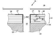
도 5는 도 4의 조작기 디바이스에서 이용하기 위한 하나의 조작기(11)의 개략적인 횡단면도를 도시한다.
도 6은, 팔중극자를 형성하기 위한 8개의 전극들을 각각 포함하는 조작기들의 어레이의 제 3 예의 평면도를 도시한다.
도 7은 조작기 디바이스 내에서 이용하기 위한 조작기의 추가적인 예의 개략적인 횡단면도를 도시한다.
도 8a는 도 1의 리소그래피 시스템에서 이용하기 위한 조작기 디바이스의 개략적인 평면도를 도시한다.
도 8b는, 무비임 지역들 내의 전자 제어 회로를 개략적으로 도시한, 도 8a의 개략적인 평면도의 상세도를 도시한다.
도 9는 대전 입자 다중-빔릿 검사 장치의 개략적인 횡단면도를 도시한다.
Claims (15)
- 대전 입자 다중-빔릿 장치에 이용되는 조작기 디바이스로서, 상기 조작기 디바이스는:
기판의 평면 내의 관통 개구부들의 어레이를 포함하는 평면형 기판으로서, 상기 관통 개구부들의 어레이는 행과 열에서 규칙적으로 배열되고, 상기 관통 개구부들의 각각은 하나 이상의 대전 입자 빔릿의 통과를 위해서 배열되고, 상기 관통 개구부들의 각각은 상기 관통 개구부 주위로 배열된 다수의 전극들을 구비하고, 그리고 상기 다수의 전극들이 상기 기판 내에 또는 상기 기판 상의 평면형 전극 층에 배열되는, 평면형 기판, 그리고
각각의 관통 개구부의 다수의 전극들로 제어 신호들을 제공하기 위한 전자 제어 회로를 포함하며,
상기 전자 제어 회로는 전압을 각각의 개별적인 관통 개구부의 다수의 전극들에 제공하도록 구성되며, 각각의 관통 개구부의 전극들은 접지된 전극에 의해서 적어도 실질적으로 둘러싸이는 것인, 조작기 디바이스. - 제 1 항에 있어서, 상기 전자 제어 회로는, 적어도 실질적으로 아날로그 조정가능한 전압을 상기 각각의 개별적인 관통 개구부의 다수의 전극들에 제공하도록 구성되는 것인, 조작기 디바이스.
- 제 1 항에 있어서, 상기 평면형 기판은 웨이퍼이고, 상기 전자 제어 회로는 상기 평면형 기판 상에 집적 회로를 포함하는 것인, 조작기 디바이스.
- 제 1 항에 있어서, 상기 다수의 전극들이 상기 기판 내에 배치되고, 관통 개구부의 전극들이 상기 관통 개구부의 내측 대면 벽에 대하여 적어도 부분적으로 배치되는 것인, 조작기 디바이스.
- 제 4 항에 있어서, 상기 전극들은 상기 관통 개구부의 중심선에 실질적으로 평행한 방향으로 상기 관통 개구부 내로 연장하는 것인, 조작기 디바이스.
- 제 1 항에 있어서, 각각의 개별적인 관통 개구부는 사중극자(quadrupole) 편향기 또는 팔중극자 편향기를 포함하는, 조작기 디바이스.
- 제 1 항 내지 제 6 항 중 어느 한 항에 있어서, 상기 접지된 전극은 평면형 기판 상에 성막된 금속을 포함하는 것인, 조작기 디바이스.
- 제 7 항에 있어서, 상기 금속은 몰리브덴을 포함하는 것인, 조작기 디바이스.
- 제 7 항에 있어서, 상기 평면형 기판으로부터 멀어지는 방향을 향하는 전극들의 표면은 평면형 기판과 상기 평면형 기판으로부터 멀어지는 방향을 향하는 접지된 전극의 표면 사이의 높이에 배치되는 것인, 조작기 디바이스.
- 제 7 항에 있어서, 상기 다수의 전극들은 상기 기판 상의 평면형 전극 층에 배치되고, 평면형 기판 상의 접지된 전극의 두께는, 상기 평면형 기판 상의 평면형 전극 층의 두께보다 두꺼운 것인, 조작기 디바이스.
- 제 1 항 내지 제 6 항 중 어느 한 항에 따른 제 1 조작기 디바이스 및 제 1 항 내지 제 6 항 중 어느 한 항에 따른 제 2 조작기 디바이스를 포함하는 조작기 유닛으로서,
제 2 조작기 디바이스는 제 1 조작기 디바이스로부터 이격되고, 제 2 조작기 디바이스의 각각의 관통 개구부는 제 1 조작기 디바이스의 관통 개구부 중 하나와 일직선이 되는 것인, 조작기 유닛. - 제 11 항에 있어서, 제 1 조작기 디바이스 및 제 2 조작기 디바이스의 관통 개구부들은 반경(r)을 가지고, 상기 제 1 조작기 디바이스 및 제 2 조작기 디바이스 사이의 거리(d)는 상기 반경(r) 이하인 것인, 조작기 유닛.
- 제 11 항에 있어서, 제 1 및 제 2 조작기 디바이스의 전극들은 제 1 및 제 2 조작기 디바이스의 기판 상의 평면형 전극 층에 각각 배치되고, 상기 제 1 조작기 디바이스의 평면형 전극 층 및 상기 제 2 조작기 디바이스의 평면형 전극 층은 서로 대면하는 것인, 조작기 유닛.
- 제 11 항에 있어서, 제 2 조작기 디바이스는 제 1 조작기 디바이스와 제 2 조작기 디바이스 사이의 중심 평면에 관하여 제 1 조작기 디바이스에 대해 거울 대칭인 것인, 조작기 유닛.
- 광학 컬럼을 포함하는 대전 입자 다중 빔릿 장치로서,
확장하는 대전 입자 비임을 생성하는 대전 입자 공급원,
대전 입자 비임을 시준하는 시준기 렌즈,
타겟을 노광하기 위한 다중 빔릿들을 생성하는 개구 어레이,
빔릿들의 그룹 내의 개별적인 빔릿들을 특정 시기에 편향시켜 블랭크하는 빔릿 블랭커 어레이,
편향된 개별적인 빔릿들을 중단하는 빔 중단부 어레이, 및
중단되지 않은 빔릿을 타겟으로 투사하는 투사 렌즈 시스템
을 포함하고
다중 빔릿 각각은 빔릿 블랭커 어레이에 의해 블랭크되지 않는 경우에 타겟을 노광하며,
상기 대전 입자 다중 빔릿 장치는 이 대전 입자 다중 빔릿 장치 내에서 복수의 대전 입자 빔릿 중 하나 이상의 대전 입자 비임들의 조작을 위한 조작기 디바이스를 포함하고,
상기 조작기 디바이스는
평면형 기판의 평면의 관통 개구부들의 어레이를 포함하는 상기 평면형 기판으로서, 상기 관통 개구부들의 어레이는 행과 열에서 규칙적으로 배열되고, 상기 관통 개구부들의 각각은 하나 이상의 대전 입자 빔릿을 통과시키도록 배치되고, 관통 개구부들의 각각은 관통 개구부 주위로 배치된 다수의 전극들을 구비하고, 다수의 전극들이 상기 기판 내에 또는 기판 상의 평면형 전극 층에 배치되는, 평면형 기판과,
각각의 관통 개구부의 다수의 전극들에 제어 신호를 제공하는 전자 제어 회로
를 포함하며, 상기 전자 제어 회로는 전압을 각각의 개별적인 관통 개구부의 다수의 전극들에 제공하도록 구성되며, 각각의 관통 개구부의 전극들은 접지된 전극에 의해서 적어도 실질적으로 둘러싸이는 것인, 대전 입자 다중 빔릿 장치.
Priority Applications (1)
| Application Number | Priority Date | Filing Date | Title |
|---|---|---|---|
| KR1020227002799A KR102553059B1 (ko) | 2011-05-30 | 2012-05-30 | 대전 입자 다중-빔릿 장치 |
Applications Claiming Priority (6)
| Application Number | Priority Date | Filing Date | Title |
|---|---|---|---|
| NL2006868A NL2006868C2 (en) | 2011-05-30 | 2011-05-30 | Charged particle multi-beamlet apparatus. |
| NL2006868 | 2011-05-30 | ||
| US201161491865P | 2011-05-31 | 2011-05-31 | |
| US61/491,865 | 2011-05-31 | ||
| PCT/NL2012/050376 WO2012165955A2 (en) | 2011-05-30 | 2012-05-30 | Charged particle multi-beamlet apparatus |
| KR1020207005591A KR102137169B1 (ko) | 2011-05-30 | 2012-05-30 | 대전 입자 다중-빔릿 장치 |
Related Parent Applications (1)
| Application Number | Title | Priority Date | Filing Date |
|---|---|---|---|
| KR1020207005591A Division KR102137169B1 (ko) | 2011-05-30 | 2012-05-30 | 대전 입자 다중-빔릿 장치 |
Related Child Applications (1)
| Application Number | Title | Priority Date | Filing Date |
|---|---|---|---|
| KR1020227002799A Division KR102553059B1 (ko) | 2011-05-30 | 2012-05-30 | 대전 입자 다중-빔릿 장치 |
Publications (2)
| Publication Number | Publication Date |
|---|---|
| KR20200091490A true KR20200091490A (ko) | 2020-07-30 |
| KR102357303B1 KR102357303B1 (ko) | 2022-02-08 |
Family
ID=47260136
Family Applications (7)
| Application Number | Title | Priority Date | Filing Date |
|---|---|---|---|
| KR1020237022503A Active KR102780450B1 (ko) | 2011-05-30 | 2012-05-30 | 대전 입자 다중-빔릿 장치 |
| KR1020207020901A Active KR102357303B1 (ko) | 2011-05-30 | 2012-05-30 | 대전 입자 다중-빔릿 장치 |
| KR1020227002799A Active KR102553059B1 (ko) | 2011-05-30 | 2012-05-30 | 대전 입자 다중-빔릿 장치 |
| KR1020207005591A Active KR102137169B1 (ko) | 2011-05-30 | 2012-05-30 | 대전 입자 다중-빔릿 장치 |
| KR1020197026754A Active KR102084040B1 (ko) | 2011-05-30 | 2012-05-30 | 대전 입자 다중-빔릿 장치 |
| KR1020187008117A Active KR102023054B1 (ko) | 2011-05-30 | 2012-05-30 | 대전 입자 다중-빔릿 장치 |
| KR1020137034251A Active KR101842710B1 (ko) | 2011-05-30 | 2012-05-30 | 대전 입자 다중 빔릿 장치 |
Family Applications Before (1)
| Application Number | Title | Priority Date | Filing Date |
|---|---|---|---|
| KR1020237022503A Active KR102780450B1 (ko) | 2011-05-30 | 2012-05-30 | 대전 입자 다중-빔릿 장치 |
Family Applications After (5)
| Application Number | Title | Priority Date | Filing Date |
|---|---|---|---|
| KR1020227002799A Active KR102553059B1 (ko) | 2011-05-30 | 2012-05-30 | 대전 입자 다중-빔릿 장치 |
| KR1020207005591A Active KR102137169B1 (ko) | 2011-05-30 | 2012-05-30 | 대전 입자 다중-빔릿 장치 |
| KR1020197026754A Active KR102084040B1 (ko) | 2011-05-30 | 2012-05-30 | 대전 입자 다중-빔릿 장치 |
| KR1020187008117A Active KR102023054B1 (ko) | 2011-05-30 | 2012-05-30 | 대전 입자 다중-빔릿 장치 |
| KR1020137034251A Active KR101842710B1 (ko) | 2011-05-30 | 2012-05-30 | 대전 입자 다중 빔릿 장치 |
Country Status (9)
| Country | Link |
|---|---|
| US (1) | US9607806B2 (ko) |
| EP (2) | EP3660883B1 (ko) |
| JP (1) | JP6141276B2 (ko) |
| KR (7) | KR102780450B1 (ko) |
| CN (1) | CN103650097B (ko) |
| NL (1) | NL2006868C2 (ko) |
| RU (1) | RU2632937C2 (ko) |
| TW (1) | TWI582816B (ko) |
| WO (1) | WO2012165955A2 (ko) |
Families Citing this family (138)
| Publication number | Priority date | Publication date | Assignee | Title |
|---|---|---|---|---|
| JP6147528B2 (ja) * | 2012-06-01 | 2017-06-14 | 株式会社ニューフレアテクノロジー | マルチ荷電粒子ビーム描画方法及びマルチ荷電粒子ビーム描画装置 |
| US9824851B2 (en) * | 2013-01-20 | 2017-11-21 | William M. Tong | Charge drain coating for electron-optical MEMS |
| JP6293435B2 (ja) * | 2013-08-08 | 2018-03-14 | 株式会社ニューフレアテクノロジー | マルチ荷電粒子ビーム描画装置及びマルチ荷電粒子ビーム描画方法 |
| NL2011401C2 (en) * | 2013-09-06 | 2015-03-09 | Mapper Lithography Ip Bv | Charged particle optical device. |
| DE102014008083B9 (de) | 2014-05-30 | 2018-03-22 | Carl Zeiss Microscopy Gmbh | Teilchenstrahlsystem |
| DE102014008105B4 (de) | 2014-05-30 | 2021-11-11 | Carl Zeiss Multisem Gmbh | Mehrstrahl-Teilchenmikroskop |
| DE102014008383B9 (de) | 2014-06-06 | 2018-03-22 | Carl Zeiss Microscopy Gmbh | Teilchenstrahlsystem und Verfahren zum Betreiben einer Teilchenoptik |
| US10497536B2 (en) * | 2016-09-08 | 2019-12-03 | Rockwell Collins, Inc. | Apparatus and method for correcting arrayed astigmatism in a multi-column scanning electron microscopy system |
| US10840056B2 (en) * | 2017-02-03 | 2020-11-17 | Kla Corporation | Multi-column scanning electron microscopy system |
| WO2018197169A1 (en) | 2017-04-28 | 2018-11-01 | Asml Netherlands B.V. | An apparatus using multiple beams of charged particles |
| KR102649183B1 (ko) * | 2017-10-02 | 2024-03-21 | 에이에스엠엘 네델란즈 비.브이. | 하전 입자 빔들을 사용하는 장치 |
| EP3474308A1 (en) * | 2017-10-17 | 2019-04-24 | Universiteit Antwerpen | Spatial phase manipulation of charged particle beam |
| JP7198092B2 (ja) * | 2018-05-18 | 2022-12-28 | 株式会社ニューフレアテクノロジー | マルチ電子ビーム照射装置、マルチ電子ビーム検査装置及びマルチ電子ビーム照射方法 |
| EP3576128A1 (en) * | 2018-05-28 | 2019-12-04 | ASML Netherlands B.V. | Electron beam apparatus, inspection tool and inspection method |
| US10483080B1 (en) * | 2018-07-17 | 2019-11-19 | ICT Integrated Circuit Testing Gesellschaft für Halbleiterprüftechnik mbH | Charged particle beam device, multi-beam blanker for a charged particle beam device, and method for operating a charged particle beam device |
| DE102018007652B4 (de) * | 2018-09-27 | 2021-03-25 | Carl Zeiss Multisem Gmbh | Teilchenstrahl-System sowie Verfahren zur Stromregulierung von Einzel-Teilchenstrahlen |
| US11145485B2 (en) * | 2018-12-26 | 2021-10-12 | Nuflare Technology, Inc. | Multiple electron beams irradiation apparatus |
| US20200303156A1 (en) * | 2019-03-20 | 2020-09-24 | ICT Integrated Circuit Testing Gesellschaft für Halbleiterprüftechnik mbH | Beam splitter for a charged particle device |
| EP3716313A1 (en) * | 2019-03-28 | 2020-09-30 | ASML Netherlands B.V. | Aperture array with integrated current measurement |
| EP3953959A1 (en) * | 2019-04-06 | 2022-02-16 | ASML Netherlands B.V. | Mems image forming element with built-in voltage generator |
| DE102019005362A1 (de) * | 2019-07-31 | 2021-02-04 | Carl Zeiss Multisem Gmbh | Verfahren zum Betreiben eines Vielzahl-Teilchenstrahlsystems unter Veränderung der numerischen Apertur, zugehöriges Computerprogrammprodukt und Vielzahl-Teilchenstrahlsystem |
| JP7222874B2 (ja) * | 2019-11-12 | 2023-02-15 | 東芝デバイス&ストレージ株式会社 | 半導体装置 |
| US11120965B2 (en) * | 2019-12-04 | 2021-09-14 | ICT Integrated Circuit Testing Gesellschaft für Halbleiterprüftechnik mbH | Beam blanking device for a multi-beamlet charged particle beam apparatus |
| EP3975222A1 (en) | 2020-09-24 | 2022-03-30 | ASML Netherlands B.V. | Charged particle assessment tool, inspection method |
| KR102830218B1 (ko) | 2020-01-06 | 2025-07-08 | 에이에스엠엘 네델란즈 비.브이. | 하전 입자 평가 툴, 검사 방법 |
| EP3937204A1 (en) | 2020-07-06 | 2022-01-12 | ASML Netherlands B.V. | Inspection apparatus |
| EP3863040A1 (en) | 2020-02-07 | 2021-08-11 | ASML Netherlands B.V. | Charged particle manipulator device |
| EP3869535A1 (en) | 2020-02-21 | 2021-08-25 | ASML Netherlands B.V. | Charged particle assessment tool, inspection method |
| EP3869536A1 (en) | 2020-02-21 | 2021-08-25 | ASML Netherlands B.V. | Inspection apparatus |
| EP3869533A1 (en) | 2020-02-21 | 2021-08-25 | ASML Netherlands B.V. | Charged particle assessment tool, inspection method |
| IL295627A (en) | 2020-02-21 | 2022-10-01 | Asml Netherlands Bv | Inspection apparatus |
| KR102817129B1 (ko) | 2020-02-21 | 2025-06-05 | 에이에스엠엘 네델란즈 비.브이. | 하전 입자 검사 툴, 검사 방법 |
| EP3876258A1 (en) * | 2020-03-06 | 2021-09-08 | ASML Netherlands B.V. | Beam manipulator in charged particle-beam exposure apparatus |
| JP7359050B2 (ja) * | 2020-03-18 | 2023-10-11 | 株式会社ニューフレアテクノロジー | マルチビーム用のブランキング装置及びマルチ荷電粒子ビーム描画装置 |
| EP3893264A1 (en) | 2020-04-06 | 2021-10-13 | ASML Netherlands B.V. | Charged particle assessment tool, inspection method |
| EP3893263A1 (en) * | 2020-04-06 | 2021-10-13 | ASML Netherlands B.V. | Aperture assembly, beam manipulator unit, method of manipulating charged particle beams, and charged particle projection apparatus |
| JP7409946B2 (ja) * | 2020-04-13 | 2024-01-09 | 株式会社ニューフレアテクノロジー | マルチ荷電粒子ビーム照射装置及びマルチ荷電粒子ビーム検査装置 |
| IL298348A (en) | 2020-06-10 | 2023-01-01 | Asml Netherlands Bv | Interchangeable module for charged particle device |
| EP4020565A1 (en) | 2020-12-23 | 2022-06-29 | ASML Netherlands B.V. | Detector substrate, an inspection apparatus and method of sample assessment |
| KR102827024B1 (ko) | 2020-07-06 | 2025-07-02 | 에이에스엠엘 네델란즈 비.브이. | 하전 입자 다중-빔 평가 도구에 사용하기 위한 검출기 기판 |
| EP3937205A1 (en) * | 2020-07-06 | 2022-01-12 | ASML Netherlands B.V. | Charged-particle multi-beam column, charged-particle multi-beam column array, inspection method |
| IL300807A (en) | 2020-09-17 | 2023-04-01 | Asml Netherlands Bv | Charged particle evaluation tool test method |
| EP3971939A1 (en) | 2020-09-17 | 2022-03-23 | ASML Netherlands B.V. | Charged particle assessment tool, inspection method |
| EP4214737A1 (en) | 2020-09-17 | 2023-07-26 | ASML Netherlands B.V. | Objective lens array assembly, electron-optical system, electron-optical system array, method of focusing, objective lens arrangement |
| EP3971940A1 (en) | 2020-09-17 | 2022-03-23 | ASML Netherlands B.V. | Objective lens array assembly, electron-optical system, electron-optical system array, method of focusing, objective lens arrangement |
| IL302654A (en) | 2020-11-12 | 2023-07-01 | Asml Netherlands Bv | Assembling an objective lens array, electronic-optical system, electronic-optical system array, focusing method |
| EP4002421A1 (en) | 2020-11-12 | 2022-05-25 | ASML Netherlands B.V. | Objective lens array assembly, electron-optical system, electron-optical system array, method of focusing |
| EP4009348A1 (en) | 2020-12-01 | 2022-06-08 | ASML Netherlands B.V. | Charged particle inspection tool and method |
| EP4009349A1 (en) | 2020-12-03 | 2022-06-08 | ASML Netherlands B.V. | Charged particle tool, calibration method, inspection method |
| IL303577A (en) | 2020-12-14 | 2023-08-01 | Asml Netherlands Bv | Charged particle system, a sample processing method using multiple beams of charged particles |
| EP4086933A1 (en) | 2021-05-03 | 2022-11-09 | ASML Netherlands B.V. | Charged particle system, method of processing a sample using a multi-beam of charged particles |
| JP2024501654A (ja) | 2020-12-23 | 2024-01-15 | エーエスエムエル ネザーランズ ビー.ブイ. | 荷電粒子光学デバイス |
| EP4020516A1 (en) | 2020-12-23 | 2022-06-29 | ASML Netherlands B.V. | Charged particle optical device, objective lens assembly, detector, detector array, and methods |
| WO2022139689A1 (en) * | 2020-12-24 | 2022-06-30 | National University Of Singapore | Ion microscope |
| EP4084039A1 (en) | 2021-04-29 | 2022-11-02 | ASML Netherlands B.V. | Charged particle assessment system and method |
| IL308010A (en) | 2021-05-12 | 2023-12-01 | Asml Netherlands Bv | Evaluation system, evaluation method |
| EP4089712A1 (en) | 2021-05-12 | 2022-11-16 | ASML Netherlands B.V. | Assessment system, method of assessing |
| EP4092712A1 (en) * | 2021-05-18 | 2022-11-23 | ASML Netherlands B.V. | Charged particle optical device and method using it |
| EP4092614A1 (en) | 2021-05-21 | 2022-11-23 | ASML Netherlands B.V. | Data processing device and method, charged particle assessment system and method |
| EP4341890A1 (en) | 2021-05-21 | 2024-03-27 | ASML Netherlands B.V. | Data processing device and method, charged particle assessment system and method |
| EP4095881A1 (en) | 2021-05-25 | 2022-11-30 | ASML Netherlands B.V. | Charged particle device |
| EP4352773A1 (en) | 2021-06-08 | 2024-04-17 | ASML Netherlands B.V. | Charged particle apparatus and method |
| EP4102535A1 (en) | 2021-06-08 | 2022-12-14 | ASML Netherlands B.V. | Charged particle apparatus and method |
| EP4102536A1 (en) | 2021-06-10 | 2022-12-14 | ASML Netherlands B.V. | Method of compensating for an effect of electrode distortion, assessment system |
| EP4113570A1 (en) | 2021-06-29 | 2023-01-04 | ASML Netherlands B.V. | Charged particle assessment system and method of aligning a sample in a charged particle assessment system |
| EP4117015A1 (en) | 2021-07-05 | 2023-01-11 | ASML Netherlands B.V. | Charged particle device, detector, and methods |
| EP4117016A1 (en) | 2021-07-05 | 2023-01-11 | ASML Netherlands B.V. | Charged particle detector |
| EP4117017A1 (en) | 2021-07-05 | 2023-01-11 | ASML Netherlands B.V. | Charged particle detector |
| EP4117014A1 (en) | 2021-07-07 | 2023-01-11 | ASML Netherlands B.V. | Charged particle apparatus and method |
| WO2023280551A1 (en) | 2021-07-07 | 2023-01-12 | Asml Netherlands B.V. | Charged particle apparatus and method |
| EP4117012A1 (en) | 2021-07-07 | 2023-01-11 | ASML Netherlands B.V. | Charged particle-optical device, charged particle apparatus and method |
| DE102021118561B4 (de) | 2021-07-19 | 2023-03-30 | Carl Zeiss Multisem Gmbh | Verfahren zum Betreiben eines Vielstrahl-Teilchenmikroskopes mit schneller Strahlstromregelung, Computerprogrammprodukt und Vielstrahl-Teilchenmikroskop |
| EP4123683A1 (en) | 2021-07-20 | 2023-01-25 | ASML Netherlands B.V. | Data processing device and method, charged particle assessment system and method |
| EP4131329A1 (en) | 2021-08-02 | 2023-02-08 | ASML Netherlands B.V. | Charged-particle optical device |
| EP4156227A1 (en) | 2021-09-27 | 2023-03-29 | ASML Netherlands B.V. | Charged particle apparatus and method |
| US11651934B2 (en) | 2021-09-30 | 2023-05-16 | Kla Corporation | Systems and methods of creating multiple electron beams |
| EP4170695A1 (en) | 2021-10-19 | 2023-04-26 | ASML Netherlands B.V. | Detector assembly, charged particle device, apparatus, and methods |
| KR20240093780A (ko) | 2021-10-19 | 2024-06-24 | 에이에스엠엘 네델란즈 비.브이. | 검출기 조립체, 하전 입자 디바이스, 장치, 및 방법 |
| KR20240095241A (ko) | 2021-11-11 | 2024-06-25 | 에이에스엠엘 네델란즈 비.브이. | 하전 입자 평가 시스템 및 방법 |
| EP4181167A1 (en) | 2021-11-11 | 2023-05-17 | ASML Netherlands B.V. | Charged particle assessment system and method |
| KR20240122824A (ko) | 2021-12-15 | 2024-08-13 | 에이에스엠엘 네델란즈 비.브이. | 샘플 맵을 생성하는 방법, 컴퓨터 프로그램 제품 |
| WO2023110244A1 (en) | 2021-12-15 | 2023-06-22 | Asml Netherlands B.V. | Charged particle assessment system |
| EP4213176A1 (en) | 2022-01-13 | 2023-07-19 | ASML Netherlands B.V. | Charged particle assessment system |
| WO2023110331A1 (en) | 2021-12-17 | 2023-06-22 | Asml Netherlands B.V. | Charged-particle optical apparatus and projection method |
| KR20240115321A (ko) | 2021-12-17 | 2024-07-25 | 에이에스엠엘 네델란즈 비.브이. | 검출기 검사 디바이스, 검출기 조립체, 검출기 어레이, 장치, 및 방법 |
| EP4199032A1 (en) | 2021-12-17 | 2023-06-21 | ASML Netherlands B.V. | Detector inspection device, detector assembly, detector array, apparatus, and method |
| EP4199031A1 (en) | 2021-12-17 | 2023-06-21 | ASML Netherlands B.V. | Charged-particle optical apparatus and projection method |
| EP4199027A1 (en) | 2021-12-17 | 2023-06-21 | ASML Netherlands B.V. | Charged-particle apparatus, multi-device apparatus, method of using charged-particle apparatus and control method |
| EP4199028A1 (en) | 2021-12-20 | 2023-06-21 | ASML Netherlands B.V. | Charged particle device, charged particle assessment apparatus, measuring method, and monitoring method |
| EP4199033A1 (en) | 2021-12-20 | 2023-06-21 | ASML Netherlands B.V. | Method of processing a sample with a charged particle assessment system |
| WO2023117277A1 (en) | 2021-12-23 | 2023-06-29 | Asml Netherlands B.V. | Electron-optical device, method of compensating for variations in a property of sub-beams |
| EP4202969A1 (en) | 2021-12-23 | 2023-06-28 | ASML Netherlands B.V. | Electron-optical device with compensation for variations in a property of sub-beams |
| EP4202970A1 (en) | 2021-12-24 | 2023-06-28 | ASML Netherlands B.V. | Alignment determination method and computer program |
| CN118451527A (zh) | 2021-12-31 | 2024-08-06 | Asml荷兰有限公司 | 带电粒子束装置中的束操纵器 |
| EP4250331A1 (en) | 2022-03-22 | 2023-09-27 | ASML Netherlands B.V. | Charged particle apparatus and method |
| EP4258320A1 (en) | 2022-04-08 | 2023-10-11 | ASML Netherlands B.V. | Sensor substrate, apparatus, and method |
| CN119156687A (zh) * | 2022-04-11 | 2024-12-17 | 华为技术有限公司 | 粒子矫正装置、粒子矫正器模组和粒子系统 |
| EP4280252A1 (en) | 2022-05-16 | 2023-11-22 | ASML Netherlands B.V. | Charged particle optical device and method |
| WO2023202819A1 (en) | 2022-04-18 | 2023-10-26 | Asml Netherlands B.V. | Charged particle optical device and method |
| CN119404279A (zh) | 2022-07-15 | 2025-02-07 | Asml荷兰有限公司 | 带电粒子光学装置 |
| EP4354485A1 (en) | 2022-10-13 | 2024-04-17 | ASML Netherlands B.V. | Charged particle-optical apparatus |
| EP4345861A1 (en) | 2022-09-28 | 2024-04-03 | ASML Netherlands B.V. | Charged particle apparatus |
| EP4421843A1 (en) | 2023-02-27 | 2024-08-28 | ASML Netherlands B.V. | Charged particle-optical apparatus |
| IL320209A (en) | 2022-10-27 | 2025-06-01 | Asml Netherlands Bv | Charged particle-optical apparatus |
| DE102022131862A1 (de) | 2022-12-01 | 2024-06-06 | Carl Zeiss Multisem Gmbh | Vielstrahl-Teilchenmikroskop umfassend eine Aberrationskorrektureinheit mit Geometrie-basierten Korrekturelektroden und Verfahren zum Einstellen der Aberrationskorrektur sowie Computerprogrammprodukt |
| EP4391009A1 (en) | 2022-12-21 | 2024-06-26 | ASML Netherlands B.V. | Charged particle device and charged particle apparatus |
| US12451322B2 (en) * | 2023-02-15 | 2025-10-21 | ICT Integrated Circuit Testing Gesellschaft für Halbleiterprüftechnik mbH | Method of forming a multipole device, method of influencing an electron beam, and multipole device |
| EP4418302A1 (en) * | 2023-02-16 | 2024-08-21 | ASML Netherlands B.V. | Charged particle-optical element, charged particle-optical module, assessment apparatus, chip assembly, method of manufacturing |
| DE102023202582A1 (de) * | 2023-03-22 | 2024-09-26 | Carl Zeiss Multisem Gmbh | Verbesserte Vielstrahl-Erzeugungseinrichtung und Methode zum Betrieb einer Vielstrahl-Erzeugungseinrichtung |
| EP4539091A1 (en) | 2023-10-10 | 2025-04-16 | ASML Netherlands B.V. | Electron-beam imaging system |
| EP4576159A1 (en) | 2023-12-20 | 2025-06-25 | ASML Netherlands B.V. | Charged particle system and method of baking out a charged particle system |
| TW202536906A (zh) | 2023-11-09 | 2025-09-16 | 荷蘭商Asml荷蘭公司 | 帶電粒子系統及烘乾帶電粒子系統之方法 |
| EP4567474A1 (en) | 2023-12-08 | 2025-06-11 | ASML Netherlands B.V. | Signal processing method, signal processor, assessment method, and assessment apparatus |
| EP4576158A1 (en) | 2023-12-18 | 2025-06-25 | ASML Netherlands B.V. | Charged particle-optical module, charged particle-optical device, and a method of using a charged-particle apparatus |
| EP4597540A1 (en) | 2024-01-30 | 2025-08-06 | ASML Netherlands B.V. | Charged particle-optical apparatus and method of processing a sample |
| EP4576157A1 (en) | 2023-12-20 | 2025-06-25 | ASML Netherlands B.V. | High-voltage discharge detection in a charged particle system |
| WO2025131457A1 (en) | 2023-12-20 | 2025-06-26 | Asml Netherlands B.V. | Method and apparatus for assessing a sample surface, method of scanning a sample surface, and charged particle assessment apparatus |
| EP4575637A1 (en) | 2023-12-20 | 2025-06-25 | ASML Netherlands B.V. | Method and apparatus for assessing a sample surface, method of scanning a sample surface, and charged particle assessment apparatus |
| WO2025131442A1 (en) | 2023-12-20 | 2025-06-26 | Asml Netherlands B.V. | Charged particle-optical apparatus and method of processing a sample |
| WO2025201803A1 (en) | 2024-03-28 | 2025-10-02 | Asml Netherlands B.V. | Charged particle-optical module |
| WO2025201807A1 (en) | 2024-03-28 | 2025-10-02 | Asml Netherlands B.V. | Charged particle-optical module |
| WO2025201790A1 (en) | 2024-03-28 | 2025-10-02 | Asml Netherlands B.V. | Charged particle-optical module |
| WO2025201789A1 (en) | 2024-03-28 | 2025-10-02 | Asml Netherlands B.V. | Charged particle-optical module |
| WO2025201804A1 (en) | 2024-03-28 | 2025-10-02 | Asml Netherlands B.V. | Charged particle-optical module |
| WO2025201799A1 (en) | 2024-03-28 | 2025-10-02 | Asml Netherlands B.V. | Charged particle-optical module |
| WO2025224235A2 (en) * | 2024-04-25 | 2025-10-30 | Carl Zeiss Multisem Gmbh | Improved beam control for a multi-beam scanning particle imaging system |
| WO2025261658A1 (en) | 2024-06-18 | 2025-12-26 | Asml Netherlands B.V. | Systems and methods for handling the impact of failing beams in multibeam inspection |
| EP4672297A1 (en) | 2024-06-26 | 2025-12-31 | ASML Netherlands B.V. | ELECTROSTATIC LENS |
| EP4685837A1 (en) | 2024-07-25 | 2026-01-28 | ASML Netherlands B.V. | Charged particle-optical element, charged particle-optical device and methods of manufacturing electrodes |
| EP4723158A1 (en) | 2024-10-02 | 2026-04-08 | ASML Netherlands B.V. | Charged particle-optical device and method of assessing |
| EP4726766A1 (en) | 2024-10-10 | 2026-04-15 | ASML Netherlands B.V. | Charged particle-optical apparatus |
| EP4726765A1 (en) | 2024-10-10 | 2026-04-15 | ASML Netherlands B.V. | Charged particle assessment system and method |
| EP4553886A3 (en) | 2025-03-28 | 2025-12-24 | ASML Netherlands B.V. | Optical beam member |
| EP4571811A2 (en) | 2025-04-30 | 2025-06-18 | ASML Netherlands B.V. | Cross talk reduction |
| EP4576149A3 (en) | 2025-05-02 | 2025-11-19 | ASML Netherlands B.V. | Electrical connection system |
| EP4589629A3 (en) | 2025-05-15 | 2026-02-25 | ASML Netherlands B.V. | Assessment apparatus and method for assessment |
| EP4593056A3 (en) | 2025-06-13 | 2025-12-24 | ASML Netherlands B.V. | Optical beam member |
| EP4683140A1 (en) | 2025-07-24 | 2026-01-21 | ASML Netherlands B.V. | Method of forming a cable termination and cable |
Citations (4)
| Publication number | Priority date | Publication date | Assignee | Title |
|---|---|---|---|---|
| KR20030028461A (ko) * | 2000-04-04 | 2003-04-08 | 주식회사 아도반테스토 | 다축전자렌즈를 이용한 멀티빔 노광장치, 반도체소자제조방법 |
| JP2005136114A (ja) * | 2003-10-30 | 2005-05-26 | Canon Inc | 電極基板およびその製造方法、ならびに該電極基板を用いた荷電ビーム露光装置 |
| US20100065741A1 (en) * | 2005-08-24 | 2010-03-18 | Dagmar Gerthsen | Method For The Production Of Multiplayer Electrostatic Lens Array |
| WO2011051301A1 (en) * | 2009-10-26 | 2011-05-05 | Mapper Lithography Ip B.V. | Charged particle multi-beamlet lithography system, modulation device, and method of manufacturing thereof |
Family Cites Families (78)
| Publication number | Priority date | Publication date | Assignee | Title |
|---|---|---|---|---|
| JPS61190839A (ja) | 1985-02-19 | 1986-08-25 | Canon Inc | 荷電粒子線装置 |
| JPS6288247A (ja) | 1985-10-14 | 1987-04-22 | Fujitsu Ltd | 電子ビ−ム露光装置 |
| JPS63173326A (ja) | 1987-01-13 | 1988-07-16 | Fujitsu Ltd | 電子ビ−ム露光方法 |
| EP0404608B1 (en) * | 1989-05-19 | 1995-02-22 | Fujitsu Limited | Blanking aperture array, method of producing blanking aperture array, charged particle beam exposure apparatus and charged particle beam exposure method |
| JP2886277B2 (ja) | 1990-06-20 | 1999-04-26 | 富士通株式会社 | 電子ビーム露光装置 |
| JPH04328236A (ja) | 1991-04-26 | 1992-11-17 | Fujitsu Ltd | 電子ビーム露光装置 |
| JP3238487B2 (ja) | 1991-11-14 | 2001-12-17 | 富士通株式会社 | 電子ビーム装置 |
| US5401974A (en) * | 1993-03-18 | 1995-03-28 | Fujitsu Limited | Charged particle beam exposure apparatus and method of cleaning the same |
| US5528048A (en) * | 1994-03-15 | 1996-06-18 | Fujitsu Limited | Charged particle beam exposure system and method |
| JPH08115697A (ja) * | 1994-10-18 | 1996-05-07 | Hitachi Ltd | 電子顕微鏡装置 |
| US5617129A (en) | 1994-10-27 | 1997-04-01 | Xerox Corporation | Ionographic printing with a focused ion stream controllable in two dimensions |
| EP0773576A1 (en) | 1995-11-13 | 1997-05-14 | Motorola, Inc. | Electron column optics for multibeam electron lithography system |
| JP3647143B2 (ja) * | 1996-06-12 | 2005-05-11 | キヤノン株式会社 | 電子ビーム露光装置及びその露光方法 |
| EP1369896A3 (en) | 1996-03-04 | 2004-12-22 | Canon Kabushiki Kaisha | Electron beam exposure apparatus and method and device manufacturing method |
| US5962859A (en) | 1998-01-09 | 1999-10-05 | International Business Machines Corporation | Multiple variable shaped electron beam system with lithographic structure |
| JP3014380B2 (ja) * | 1998-01-09 | 2000-02-28 | インターナショナル・ビジネス・マシーンズ・コーポレイション | 複数の可変成形電子ビ―ムを使用してパタ―ンを直接書き込むシステムおよび方法 |
| US5981962A (en) | 1998-01-09 | 1999-11-09 | International Business Machines Corporation | Distributed direct write lithography system using multiple variable shaped electron beams |
| US6175122B1 (en) * | 1998-01-09 | 2001-01-16 | International Business Machines Corporation | Method for writing a pattern using multiple variable shaped electron beams |
| US6014200A (en) | 1998-02-24 | 2000-01-11 | Nikon Corporation | High throughput electron beam lithography system |
| JP3436878B2 (ja) | 1998-03-19 | 2003-08-18 | 株式会社東芝 | 荷電粒子ビーム装置 |
| US6127775A (en) | 1998-06-29 | 2000-10-03 | Xerox Corporation | Ionic display with grid focusing |
| JP2000252207A (ja) | 1998-08-19 | 2000-09-14 | Ims Ionen Mikrofab Syst Gmbh | 粒子線マルチビームリソグラフイー |
| JP3847980B2 (ja) | 1998-10-06 | 2006-11-22 | キヤノン株式会社 | 画像形成装置 |
| JP2001015428A (ja) | 1999-04-28 | 2001-01-19 | Advantest Corp | 電子ビーム露光装置 |
| KR100339140B1 (ko) | 1999-04-28 | 2002-05-31 | 히로시 오우라 | 전자빔 노출 장치 |
| JP2001076990A (ja) | 1999-08-31 | 2001-03-23 | Canon Inc | 荷電粒子線露光装置及びその制御方法 |
| JP3763446B2 (ja) | 1999-10-18 | 2006-04-05 | キヤノン株式会社 | 静電レンズ、電子ビーム描画装置、荷電ビーム応用装置、および、デバイス製造方法 |
| WO2001039243A1 (en) * | 1999-11-23 | 2001-05-31 | Ion Diagnostics, Inc. | Electron optics for multi-beam electron beam lithography tool |
| JP2001168018A (ja) * | 1999-12-13 | 2001-06-22 | Canon Inc | 荷電粒子線露光装置、荷電粒子線露光方法及び露光補正データの決定方法、該方法を適用したデバイスの製造方法。 |
| US6465795B1 (en) | 2000-03-28 | 2002-10-15 | Applied Materials, Inc. | Charge neutralization of electron beam systems |
| JP4585661B2 (ja) | 2000-03-31 | 2010-11-24 | キヤノン株式会社 | 電子光学系アレイ、荷電粒子線露光装置およびデバイス製造方法 |
| US6787780B2 (en) | 2000-04-04 | 2004-09-07 | Advantest Corporation | Multi-beam exposure apparatus using a multi-axis electron lens, fabrication method of a semiconductor device |
| JP4401614B2 (ja) | 2000-04-04 | 2010-01-20 | 株式会社アドバンテスト | 多軸電子レンズを用いたマルチビーム露光装置、複数の電子ビームを集束する多軸電子レンズ、半導体素子製造方法 |
| EP2587515A1 (en) | 2000-06-27 | 2013-05-01 | Ebara Corporation | Inspection system by charged particle beam and method of manufacturing devices using the system |
| JP2002118060A (ja) | 2000-07-27 | 2002-04-19 | Toshiba Corp | 荷電ビーム露光装置、荷電ビーム露光方法、露光データ作成方法、露光データを作成するプログラムを記録したコンピュータ読取り可能な記録媒体、及び、露光データを記録したコンピュータ読取り可能な記録媒体 |
| DE10147133A1 (de) * | 2000-10-03 | 2002-06-13 | Advantest Corp | Elektronenstrahl-Belichtungsvorrichtung |
| US6855929B2 (en) * | 2000-12-01 | 2005-02-15 | Ebara Corporation | Apparatus for inspection with electron beam, method for operating same, and method for manufacturing semiconductor device using former |
| US6815875B2 (en) | 2001-02-27 | 2004-11-09 | Hewlett-Packard Development Company, L.P. | Electron source having planar emission region and focusing structure |
| US6563124B2 (en) | 2001-03-21 | 2003-05-13 | Applied Materials, Inc. | Electron beam apparatus having traversing circuit boards |
| JP3703774B2 (ja) * | 2002-03-28 | 2005-10-05 | 株式会社東芝 | 荷電ビーム露光装置、荷電ビームを用いた露光方法およびこの露光方法を用いた半導体装置の製造方法 |
| JP2004055933A (ja) * | 2002-07-22 | 2004-02-19 | Advantest Corp | 電子ビーム露光装置、及び電子ビーム計測モジュール |
| CN101414534B (zh) * | 2002-10-30 | 2012-10-03 | 迈普尔平版印刷Ip有限公司 | 电子束曝光系统 |
| JP2004165076A (ja) * | 2002-11-15 | 2004-06-10 | Advantest Corp | 偏向器の製造方法、偏向器、及び露光装置 |
| DE60236302D1 (de) * | 2002-12-17 | 2010-06-17 | Integrated Circuit Testing | Mehrachsige Verbundlinse, Strahlvorrichtung und Verfahren zur Anwendung dieser kombinierten Linse |
| GB2397691B (en) | 2003-01-24 | 2005-08-10 | Leica Microsys Lithography Ltd | Cooling of a device for influencing an electron beam |
| JP2004282038A (ja) | 2003-02-28 | 2004-10-07 | Canon Inc | 偏向器、偏向器を製造する方法、偏向器を適用した荷電粒子線露光装置 |
| DE602004010824T2 (de) | 2003-07-30 | 2008-12-24 | Mapper Lithography Ip B.V. | Modulator-schaltkreise |
| JP4738723B2 (ja) * | 2003-08-06 | 2011-08-03 | キヤノン株式会社 | マルチ荷電粒子線描画装置、荷電粒子線の電流の測定方法及びデバイス製造方法 |
| JP4459568B2 (ja) * | 2003-08-06 | 2010-04-28 | キヤノン株式会社 | マルチ荷電ビームレンズおよびそれを用いた荷電ビーム露光装置 |
| JP3889743B2 (ja) * | 2003-12-05 | 2007-03-07 | 株式会社東芝 | 荷電ビーム描画方法及び描画装置 |
| GB2413694A (en) * | 2004-04-30 | 2005-11-02 | Ims Nanofabrication Gmbh | Particle-beam exposure apparatus |
| KR101099487B1 (ko) | 2004-05-17 | 2011-12-28 | 마퍼 리쏘그라피 아이피 비.브이. | 대전 입자 빔 노광 시스템 |
| JP4477434B2 (ja) * | 2004-06-29 | 2010-06-09 | キヤノン株式会社 | 荷電粒子線露光装置およびデバイス製造方法 |
| JP4704702B2 (ja) | 2004-06-30 | 2011-06-22 | キヤノン株式会社 | ブランキングアパーチャアレイおよびその製造方法 |
| JP2006079911A (ja) * | 2004-09-09 | 2006-03-23 | Hitachi High-Technologies Corp | 電子ビーム電流計測方法、電子ビーム描画装置および電子ビーム検出器 |
| WO2006053358A1 (en) * | 2004-11-17 | 2006-05-26 | Ims Nanofabrication Ag | Pattern lock system for particle-beam exposure apparatus |
| JP4648087B2 (ja) * | 2005-05-25 | 2011-03-09 | キヤノン株式会社 | 偏向器の作製方法、荷電粒子線露光装置、および、デバイス製造方法 |
| JP4679978B2 (ja) * | 2005-06-28 | 2011-05-11 | 株式会社日立ハイテクノロジーズ | 荷電粒子ビーム応用装置 |
| DE602005012945D1 (de) * | 2005-07-20 | 2009-04-09 | Zeiss Carl Sms Gmbh | Teilchenstrahlbelichtungssystem und Vorrichtung zur Strahlbeeinflussung |
| US8890095B2 (en) * | 2005-07-25 | 2014-11-18 | Mapper Lithography Ip B.V. | Reliability in a maskless lithography system |
| US7868300B2 (en) * | 2005-09-15 | 2011-01-11 | Mapper Lithography Ip B.V. | Lithography system, sensor and measuring method |
| JP5103033B2 (ja) * | 2007-03-02 | 2012-12-19 | 株式会社日立ハイテクノロジーズ | 荷電粒子線応用装置 |
| US7755061B2 (en) * | 2007-11-07 | 2010-07-13 | Kla-Tencor Technologies Corporation | Dynamic pattern generator with cup-shaped structure |
| KR101570974B1 (ko) | 2008-02-26 | 2015-11-23 | 마퍼 리쏘그라피 아이피 비.브이. | 투사 렌즈 배열체 |
| US8445869B2 (en) * | 2008-04-15 | 2013-05-21 | Mapper Lithography Ip B.V. | Projection lens arrangement |
| JP2009218474A (ja) * | 2008-03-12 | 2009-09-24 | Jeol Ltd | ビーム位置ドリフト抑制方法、ビーム寸法ドリフト抑制方法及び荷電粒子ビーム描画装置。 |
| WO2009127659A2 (en) * | 2008-04-15 | 2009-10-22 | Mapper Lithography Ip B.V. | Beamlet blanker arrangement |
| US8258484B2 (en) * | 2008-04-15 | 2012-09-04 | Mapper Lithography Ip B.V. | Beamlet blanker arrangement |
| KR101649106B1 (ko) * | 2008-10-01 | 2016-08-19 | 마퍼 리쏘그라피 아이피 비.브이. | 정전기 렌즈 구조 |
| DE102008062450B4 (de) * | 2008-12-13 | 2012-05-03 | Vistec Electron Beam Gmbh | Anordnung zur Beleuchtung eines Substrats mit mehreren individuell geformten Partikelstrahlen zur hochauflösenden Lithographie von Strukturmustern |
| CN102422380A (zh) | 2009-02-22 | 2012-04-18 | 迈普尔平版印刷Ip有限公司 | 带电粒子微影设备及真空腔室中产生真空的方法 |
| TWI497557B (zh) | 2009-04-29 | 2015-08-21 | Mapper Lithography Ip Bv | 包含靜電偏轉器的帶電粒子光學系統 |
| CN102460631B (zh) * | 2009-05-20 | 2015-03-25 | 迈普尔平版印刷Ip有限公司 | 两次扫描 |
| US8624478B2 (en) | 2009-10-09 | 2014-01-07 | Mapper Lithography Ip B.V. | High voltage shielding arrangement of a charged particle lithography system |
| US8546767B2 (en) * | 2010-02-22 | 2013-10-01 | Ims Nanofabrication Ag | Pattern definition device with multiple multibeam array |
| US20120065741A1 (en) * | 2010-09-13 | 2012-03-15 | Chao-Fu Chang | Guided tissue regeneration membrane |
| WO2012041464A1 (en) | 2010-09-28 | 2012-04-05 | Applied Materials Israel Ltd. | Particle-optical systems and arrangements and particle-optical components for such systems and arrangements |
| RU113611U1 (ru) | 2011-05-05 | 2012-02-20 | Александр Сергеевич Бердников | Устройство для манипулирования заряженными частицами |
-
2011
- 2011-05-30 NL NL2006868A patent/NL2006868C2/en active
-
2012
- 2012-05-30 WO PCT/NL2012/050376 patent/WO2012165955A2/en not_active Ceased
- 2012-05-30 KR KR1020237022503A patent/KR102780450B1/ko active Active
- 2012-05-30 KR KR1020207020901A patent/KR102357303B1/ko active Active
- 2012-05-30 TW TW101119563A patent/TWI582816B/zh active
- 2012-05-30 RU RU2013157921A patent/RU2632937C2/ru active
- 2012-05-30 EP EP19216208.9A patent/EP3660883B1/en active Active
- 2012-05-30 US US13/484,231 patent/US9607806B2/en active Active
- 2012-05-30 CN CN201280034520.3A patent/CN103650097B/zh active Active
- 2012-05-30 KR KR1020227002799A patent/KR102553059B1/ko active Active
- 2012-05-30 JP JP2014523884A patent/JP6141276B2/ja active Active
- 2012-05-30 KR KR1020207005591A patent/KR102137169B1/ko active Active
- 2012-05-30 EP EP12725549.5A patent/EP2715768B1/en active Active
- 2012-05-30 KR KR1020197026754A patent/KR102084040B1/ko active Active
- 2012-05-30 KR KR1020187008117A patent/KR102023054B1/ko active Active
- 2012-05-30 KR KR1020137034251A patent/KR101842710B1/ko active Active
Patent Citations (4)
| Publication number | Priority date | Publication date | Assignee | Title |
|---|---|---|---|---|
| KR20030028461A (ko) * | 2000-04-04 | 2003-04-08 | 주식회사 아도반테스토 | 다축전자렌즈를 이용한 멀티빔 노광장치, 반도체소자제조방법 |
| JP2005136114A (ja) * | 2003-10-30 | 2005-05-26 | Canon Inc | 電極基板およびその製造方法、ならびに該電極基板を用いた荷電ビーム露光装置 |
| US20100065741A1 (en) * | 2005-08-24 | 2010-03-18 | Dagmar Gerthsen | Method For The Production Of Multiplayer Electrostatic Lens Array |
| WO2011051301A1 (en) * | 2009-10-26 | 2011-05-05 | Mapper Lithography Ip B.V. | Charged particle multi-beamlet lithography system, modulation device, and method of manufacturing thereof |
Also Published As
| Publication number | Publication date |
|---|---|
| KR101842710B1 (ko) | 2018-03-28 |
| KR102553059B1 (ko) | 2023-07-10 |
| WO2012165955A2 (en) | 2012-12-06 |
| EP3660883A2 (en) | 2020-06-03 |
| US20120305798A1 (en) | 2012-12-06 |
| JP6141276B2 (ja) | 2017-06-07 |
| US9607806B2 (en) | 2017-03-28 |
| JP2014519724A (ja) | 2014-08-14 |
| TW201250757A (en) | 2012-12-16 |
| EP2715768A2 (en) | 2014-04-09 |
| KR102780450B1 (ko) | 2025-03-14 |
| KR20230107401A (ko) | 2023-07-14 |
| KR20190108187A (ko) | 2019-09-23 |
| NL2006868C2 (en) | 2012-12-03 |
| KR102357303B1 (ko) | 2022-02-08 |
| KR102023054B1 (ko) | 2019-09-20 |
| KR20140048144A (ko) | 2014-04-23 |
| WO2012165955A4 (en) | 2013-04-04 |
| KR102084040B1 (ko) | 2020-03-03 |
| RU2632937C2 (ru) | 2017-10-11 |
| EP3660883B1 (en) | 2024-07-17 |
| CN103650097B (zh) | 2017-10-10 |
| EP3660883A3 (en) | 2020-08-05 |
| TWI582816B (zh) | 2017-05-11 |
| WO2012165955A3 (en) | 2013-01-24 |
| CN103650097A (zh) | 2014-03-19 |
| KR102137169B1 (ko) | 2020-07-24 |
| KR20180033604A (ko) | 2018-04-03 |
| KR20220017525A (ko) | 2022-02-11 |
| EP2715768B1 (en) | 2020-01-22 |
| KR20200023533A (ko) | 2020-03-04 |
| RU2013157921A (ru) | 2015-07-10 |
Similar Documents
| Publication | Publication Date | Title |
|---|---|---|
| KR102137169B1 (ko) | 대전 입자 다중-빔릿 장치 | |
| TWI868407B (zh) | 電子光學設備 | |
| JP7427794B2 (ja) | 荷電粒子操作デバイス | |
| TWI867247B (zh) | 物鏡陣列總成、電子光學系統、電子光學系統陣列、聚焦方法;物鏡配置 | |
| US20120273690A1 (en) | Charged particle system comprising a manipulator device for manipulation of one or more charged particle beams | |
| JP2014519724A5 (ko) | ||
| TWI865881B (zh) | 帶電粒子評估系統及在帶電粒子評估系統中對準樣品之方法 | |
| TW202217905A (zh) | 帶電粒子評估工具及檢測方法 | |
| TW202303658A (zh) | 補償電極變形之影響的方法、評估系統 | |
| CN116547777A (zh) | 物镜阵列组件、电子光学系统、电子光学系统阵列、聚焦方法 | |
| TW202347397A (zh) | 帶電粒子光學裝置及方法 | |
| TW202431309A (zh) | 電子光學元件之對準 | |
| TW202534735A (zh) | 用於帶電粒子束設備之帶電粒子光學配置 | |
| TW202410107A (zh) | 電子光學組件 | |
| CN120019465A (zh) | 电子光学元件 |
Legal Events
| Date | Code | Title | Description |
|---|---|---|---|
| A107 | Divisional application of patent | ||
| PA0104 | Divisional application for international application |
St.27 status event code: A-0-1-A10-A18-div-PA0104 St.27 status event code: A-0-1-A10-A16-div-PA0104 |
|
| PG1501 | Laying open of application |
St.27 status event code: A-1-1-Q10-Q12-nap-PG1501 |
|
| A201 | Request for examination | ||
| P11-X000 | Amendment of application requested |
St.27 status event code: A-2-2-P10-P11-nap-X000 |
|
| P13-X000 | Application amended |
St.27 status event code: A-2-2-P10-P13-nap-X000 |
|
| PA0201 | Request for examination |
St.27 status event code: A-1-2-D10-D11-exm-PA0201 |
|
| E902 | Notification of reason for refusal | ||
| PE0902 | Notice of grounds for rejection |
St.27 status event code: A-1-2-D10-D21-exm-PE0902 |
|
| E902 | Notification of reason for refusal | ||
| PE0902 | Notice of grounds for rejection |
St.27 status event code: A-1-2-D10-D21-exm-PE0902 |
|
| P11-X000 | Amendment of application requested |
St.27 status event code: A-2-2-P10-P11-nap-X000 |
|
| P13-X000 | Application amended |
St.27 status event code: A-2-2-P10-P13-nap-X000 |
|
| E701 | Decision to grant or registration of patent right | ||
| PE0701 | Decision of registration |
St.27 status event code: A-1-2-D10-D22-exm-PE0701 |
|
| A107 | Divisional application of patent | ||
| GRNT | Written decision to grant | ||
| PA0104 | Divisional application for international application |
St.27 status event code: A-0-1-A10-A18-div-PA0104 St.27 status event code: A-0-1-A10-A16-div-PA0104 |
|
| PR0701 | Registration of establishment |
St.27 status event code: A-2-4-F10-F11-exm-PR0701 |
|
| PR1002 | Payment of registration fee |
St.27 status event code: A-2-2-U10-U12-oth-PR1002 Fee payment year number: 1 |
|
| PG1601 | Publication of registration |
St.27 status event code: A-4-4-Q10-Q13-nap-PG1601 |
|
| PR1001 | Payment of annual fee |
St.27 status event code: A-4-4-U10-U11-oth-PR1001 Fee payment year number: 4 |
|
| PR1001 | Payment of annual fee |
St.27 status event code: A-4-4-U10-U11-oth-PR1001 Fee payment year number: 5 |
|
| U11 | Full renewal or maintenance fee paid |
Free format text: ST27 STATUS EVENT CODE: A-4-4-U10-U11-OTH-PR1001 (AS PROVIDED BY THE NATIONAL OFFICE) Year of fee payment: 5 |