US4481070A - Double planarization process for multilayer metallization of integrated circuit structures - Google Patents
Double planarization process for multilayer metallization of integrated circuit structures Download PDFInfo
- Publication number
- US4481070A US4481070A US06/596,745 US59674584A US4481070A US 4481070 A US4481070 A US 4481070A US 59674584 A US59674584 A US 59674584A US 4481070 A US4481070 A US 4481070A
- Authority
- US
- United States
- Prior art keywords
- insulation
- layer
- dry etching
- metallization
- photoresist
- Prior art date
- Legal status (The legal status is an assumption and is not a legal conclusion. Google has not performed a legal analysis and makes no representation as to the accuracy of the status listed.)
- Expired - Lifetime
Links
Images




Classifications
-
- H—ELECTRICITY
- H10—SEMICONDUCTOR DEVICES; ELECTRIC SOLID-STATE DEVICES NOT OTHERWISE PROVIDED FOR
- H10P—GENERIC PROCESSES OR APPARATUS FOR THE MANUFACTURE OR TREATMENT OF DEVICES COVERED BY CLASS H10
- H10P95/00—Generic processes or apparatus for manufacture or treatments not covered by the other groups of this subclass
- H10P95/06—Planarisation of inorganic insulating materials
- H10P95/062—Planarisation of inorganic insulating materials involving a dielectric removal step
- H10P95/064—Planarisation of inorganic insulating materials involving a dielectric removal step the removal being chemical etching
-
- H—ELECTRICITY
- H10—SEMICONDUCTOR DEVICES; ELECTRIC SOLID-STATE DEVICES NOT OTHERWISE PROVIDED FOR
- H10W—GENERIC PACKAGES, INTERCONNECTIONS, CONNECTORS OR OTHER CONSTRUCTIONAL DETAILS OF DEVICES COVERED BY CLASS H10
- H10W20/00—Interconnections in chips, wafers or substrates
- H10W20/01—Manufacture or treatment
- H10W20/071—Manufacture or treatment of dielectric parts thereof
- H10W20/092—Manufacture or treatment of dielectric parts thereof by smoothing the dielectric parts
Definitions
- This invention relates to a process for making integrated circuit structures having a plurality of metallization layers. More particularly, this invention relates to an improved process of planarization to smooth an insulation layer placed between metallization layers.
- an improved process for the planarization of an integrated circuit structure which comprises: applying over a metallization layer, having one or more openings therein, a layer of insulation sufficiently thin to avoid formation of voids in the portion of the insulation applied in the openings in the metallization layer; smoothing the insulation layer by removing the high portions of the insulation by, for example, dry etching the insulation; applying a further layer of insulation over the first insulation layer; and smoothing the further layer of insulation by removing the high portions by, for example, dry etching; whereby the resultant smoothed insulation surface will be substantially planar and substantially void-free.
- FIG. 1A is a vertical cross-section of a portion of a prior art integrated circuit structure illustrating the first step of planarization with an applied layer of oxide forming a void in an opening in the metallization layer.
- FIG. 1B is a vertical cross-section of the prior art structure of FIG. 1A after the applied oxide layer has been partially etched away.
- FIG. 2A is a vertical cross-section of an integrated circuit structure having a patterned metallization layer thereon.
- FIG. 2B is a vertical cross-section of an integrated circuit structure having a first planarization insulation layer applied thereon in accordance with the invention.
- FIG. 2C is a vertical cross-section of the structure of FIG. 2A with a layer of a second material spun or deposited over the insulating layer to make a smooth transition over steps.
- FIG. 2D is a vertical cross-section of the integrated circuit structure of FIG. 2B with the second material and the insulation material partially etched away.
- FIG. 3A is a vertical cross-section of the structure of FIG. 2D having a second insulation layer applied over the partially etched away first insulation layer.
- FIG. 3B is a vertical cross-section of the structure of FIG. 3A with a further layer of a second material applied over the second insulation layer for planarity.
- FIG. 3C is a vertical cross-section of the structure of FIG. 3B subject to a second etching wherein a portion of the further layer of second material and second insulation layer have been removed.
- FIG. 4A is a vertical cross-section of the structure of FIG. 3C having a further metallization layer applied thereon and patterned to form openings in the second metallization layer.
- FIG. 4B is a vertical cross-section of the structure of FIG. 4A having an insulation layer deposited over the second metallization layer.
- FIG. 4C is a vertical cross-section of the structure of FIG. 4B having a layer of a second material applied over the insulation layer.
- FIG. 4D is a vertical cross-section of the structure of FIG. 4C subjected to a further etching to remove at least a portion of the removable material and insulation material over the second metallization layer.
- FIG. 5A is a vertical cross-section of the structure of FIG. 4D with a second insulation layer placed over the structure of FIG. 4D.
- FIG. 5B is a vertical cross-section of the structure of FIG. 5A with a further layer of a second material placed over the second insulation layer.
- FIG. 5C is a vertical cross-section of the structure of FIG. 5B after being subjected to a further etching to remove a portion of the second material and second insulation layer.
- FIG. 6 is a vertical cross-section of the structure of FIG. 5C having a third patterned metallization layer applied thereto.
- the invention provides an improved process for achieving planarization of insulation placed over metallization layers to facilitate the application of further layers of metal while avoiding discontinuities which may occur if the insulation surface, to which the further metallization layer is applied, is not sufficiently planar.
- An underlying integrated circuit structure 2 has deposited thereon a metallization layer which has been patterned to provide metal lines 6 and an opening 8.
- An insulation material such as an oxide layer 18, is applied over metal lines 6.
- opening 8 is a rather small or narrow opening between adjacent metal lines 6. Therefore, the fill-in by insulation material 18 has resulted in the formation of cusps 18a and 18b which have grown together just above the top of opening 8 leaving a trapped or void area 10 which contains no insulation material.
- a layer 22 of a second material responsive to the same smoothing technique as the insulation material is applied over insulation layer 18.
- This second material is preselected to be easily removable after the smoothing operation such as, for example, a photoresist material which may be dissolved after the dry etching process is completed.
- the two layers are then subjected to a dry etch, such as a plasma etch, to remove the upper portions of both insulation layer 18 and layer 22.
- the etchant removes a sufficient amount of insulation layer 18 to expose the void area 10 by creating an opening 9 between the now etched away cusps 18a and 18b, as seen at 14 in FIG. 1B. Furthermore, not only is opening or void 10 now exposed, but the plasma etching may further etch away a portion of layer 18 beneath void 10 and, as shown at 14, thereby unduly thinning out the amount of oxide over the underlying integrated circuit structure 2.
- FIG. 2A the process of the invention will be described and illustrated in a step by step fashion.
- an integrated circuit structure 30 is illustrated having oxide portions 32, 34, and 36 previously grown or deposited thereon.
- Metal lines 40, 42, and 44 represent a patterned metallization layer which has been applied to the structure. It will be noted that opening 46 in between metal lines 40 and 42 is considerably narrower than opening 48 between metal lines 42 and 44.
- a second metallization layer may be deposited and patterned over metal lines 40, 42, and 44, it will be necessary to provide an insulation layer having sufficient thickness for low capacitance and good breakdown and shorting protection between layers.
- This insulation layer which may be formed or applied by deposition or growth of an oxide layer, must be then planarized to provide as smooth a surface as possible for a subsequently applied metallization layer to avoid discontinuities in the second metallization layer.
- deposition or growth of insulation of sufficient thickness into the narrow opening 46, without creating a void would have been difficult.
- insulation layer 50 has been applied over metal lines 40, 42, and 44. It will immediately be noted that the cusps portions 52 and 54 of insulation layer 50 have not built up sufficiently to create a void in insulation layer 50 as in the prior art practice previously illustrated in FIG. 1A. This is because insulation layer 50 has been applied as a thin layer having a thickness which will be dependent on the spacing between the most closely spaced metal lines, such as the opening shown at 46. The more closely the metal lines are spaced together, the thinner the initial insulation layer 50 must be in accordance with the process of the invention to avoid formation of voids in the portion of the insulation material which fills the narrow openings between adjacent metal lines.
- the insulation material used conveniently may be an oxide, such as silicon dioxide.
- oxide such as silicon dioxide
- other insulation materials such as silicon nitride, alumina, or silicon oxide doped with phosphorus, may be used instead of silicon dioxide.
- the thickness of the first layer of insulation material in accordance with the invention, will be dependent upon the spacing between adjacent metal lines. The narrower the spacing between narrowly spaced apart adjacent metal lines, the thinner the first layer of insulation material must be. For example, when the spacing between two adjacent metal lines is about 2 microns, the thickness of the first layer of insulation material should be about 8000 Angstroms. If the spacing between adjacent metal lines is only about 1.5 microns, then a thickness of about 5000 Angstroms is selected for the first insulation layer.
- a layer 60 of a second material has been deposited over insulation layer 50.
- the purpose of layer 60 is to provide a material which can fill in the low portions not filled in by insulation material 50, such as shown at 56 and 58.
- the material comprising second layer 60 should be a material capable of being removed by a smoothing process such as, for example, dry etching, at relatively the same, or slightly slower, rate as insulation material 50 is being removed.
- material 60 should comprise a material, such as an organic material, which may, after the smoothing operation, be selectively removable, for example, by wet chemical means without disruption of the insulation layer.
- Photoresist material such as, for example, Shipley 1470 or Kodak 747 has been found to be etchable at about the same rate as silicon dioxide with appropriate etch conditions such as are well known to those skilled in the art when both are present together as shown in FIG. 2C.
- the smoothing process such as dry etching, the remnants of the photoresist materials still remaining may then be removed by an organic solvent which will not attack the underlying oxide layer.
- the thickness of the photoresist or other second coating layer should be sufficient to fill in the low spots or portions of the insulation layer without unduly building up the thickness of the higher portions of the insulation layer. This will vary based on the type of smoothing or removal means used to subsequently remove portions of the insulation material and any other coating material, such as photoresist, which has been placed over the insulation layer. Presuming that the two materials have been preselected to provide approximately the same removal rate, a process, such as an anisotropic dry etching as with a plasma etch will remove equal amounts of both materials.
- the photoresist material remaining will be subsequently dissolved away, it is also important that the photoresist material not be unduly thick over the raised portions of insulation to permit the etching means to remove the high portions since a removal of these high portions of the insulation material is the ultimate goal of the smoothing out step.
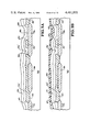
- FIG. 2D the integrated circuit structure is shown after the first smoothing step wherein oxide layer 50 and overlying photoresist material 60 have been exposed to a dry etching, such as an anisotropic reactive ion etching and the remaining photoresist material has been removed by an oxygen plasma followed by an organic solvent, such as acetone.
- a dry etching such as an anisotropic reactive ion etching
- an organic solvent such as acetone
- the foregoing steps and accompanying figures have described the first planarization stage of the double planarization process of the invention. It will be noted, at this point, that a substantially planar surface has already been created without the formation of any voids. However, due to the thinness of initial insulation layer 50 as well as its subsequent further thinning down by the etching process applied thereto, the remaining oxide layer 50' is rather thin adjacent some of the corners of the metal lines, such as shown at 64, 66, and 68 in FIG. 2D. Furthermore, as previously noted, the opening 56' remains which must be filled in before the second metallization layer may be applied.
- a second layer 70 of insulation material such as an oxide material, has been applied over insulation layer 50'. It will immediately be noted that the second insulation material has filled in the opening at 56' as well as provided a thickening of the oxides at covering over portions 64, 66, and 68.
- second insulation layer 70 may be coated with a further layer 80 of photoresist material which functions in the same manner as layer 60 in the first planarization stage.
- Second insulation layer 70 and second layer 80 are then etched as in the first planarization stage to provide a layer 70' overlying first oxide layer 50' as shown in FIG. 3C.
- the portions 64, 66, and 68, respectively overlying metal lines 40, 42, and 44 now have a sufficient thickness of oxide thereon to provide the requisite insulation.
- opening 56' has been filled and smoothed over.
- the integrated circuit structure has now been sufficiently planarized to safely permit application of a second patterned metallization layer to form metal lines 90 and 92 as shown in FIG. 4A.
- Metal lines 90 and 92 overly oxide layers 50' and 70' which will now be designated as a single insulation layer 72.
- a first insulation layer 100 has been applied over metal lines 90 and 92 forming cusps or shoulder portions 102, 104, 106, and 108.
- a layer 110 of photoresist material has been applied over insulation layer 100.
- the photoresist layer 110 fills in the portions adjacent cusps 102, 104, 106, and 108 as well as filling in at 112, the opening 109 left due to the step formed in filling in the opening between metal lines 90 and 92.
- Insulation layer 100 and photoresist layer 110 are then subject to a dry etching, as in the previous planarization stage, followed by chemical removal of the remainder of photoresist layer 110 to leave an insulation layer 100' over metal lines 90 and 92 as shown in FIG. 4D.
- a second oxide layer 120 is now applied over insulation layer 100' as shown in FIG. 5A followed, optionally, by deposition of a photoresist layer 130 as shown in FIG. 5B. Insulation layer 120 and optional photoresist layer 130 are then subjected to a further dry etching stage followed by selective removal of photoresist layer 130, if present, to provide a second oxide layer 120' over first oxide layer 100'. Layers 120' and 100' may now have applied thereto a layer of insulation 134 followed by application of yet another metallization layer which is patterned to provide metal lines 140 and 142 as shown in FIG. 6.
- the two stage planarization process of the invention which has just been described may be used at one level of the manufacturing of the integrated circuit structure together with a single planarization process at another level of metallization if, for example, an overlying metallization layer does not have as small a metal line pitch or as close spacing between the metal lines as in the underlying metallization layer.
- an overlying metallization layer does not have as small a metal line pitch or as close spacing between the metal lines as in the underlying metallization layer.
- the novel process of the invention provides for planarization of an insulation layer placed over metal lines whereby subsequent metallization layers may be placed over the oxide layer without the risk of discontinuities.
- the novel two stage planarization due to the novel two stage planarization, the occurrence of voids, particularly in the deposition of insulation material in the openings created between narrowly spaced metal lines is avoided.
Landscapes
- Internal Circuitry In Semiconductor Integrated Circuit Devices (AREA)
- Local Oxidation Of Silicon (AREA)
- Non-Metallic Protective Coatings For Printed Circuits (AREA)
- Drying Of Semiconductors (AREA)
Priority Applications (4)
| Application Number | Priority Date | Filing Date | Title |
|---|---|---|---|
| US06/596,745 US4481070A (en) | 1984-04-04 | 1984-04-04 | Double planarization process for multilayer metallization of integrated circuit structures |
| JP60501435A JPS61501738A (ja) | 1984-04-04 | 1985-03-19 | 集積回路構造の多層メタライゼ−ションのためのダブル平面化方法 |
| PCT/US1985/000485 WO1985004623A1 (fr) | 1984-04-04 | 1985-03-19 | Procede en deux etapes permettant de rendre planes des structures de circuits integres en vue de leur metallisation multicouche |
| EP19850901810 EP0177571A4 (fr) | 1984-04-04 | 1985-03-19 | Procede en deux etapes permettant de rendre planes des structures de circuits integres en vue de leur metallisation multicouche. |
Applications Claiming Priority (1)
| Application Number | Priority Date | Filing Date | Title |
|---|---|---|---|
| US06/596,745 US4481070A (en) | 1984-04-04 | 1984-04-04 | Double planarization process for multilayer metallization of integrated circuit structures |
Publications (1)
| Publication Number | Publication Date |
|---|---|
| US4481070A true US4481070A (en) | 1984-11-06 |
Family
ID=24388528
Family Applications (1)
| Application Number | Title | Priority Date | Filing Date |
|---|---|---|---|
| US06/596,745 Expired - Lifetime US4481070A (en) | 1984-04-04 | 1984-04-04 | Double planarization process for multilayer metallization of integrated circuit structures |
Country Status (4)
| Country | Link |
|---|---|
| US (1) | US4481070A (fr) |
| EP (1) | EP0177571A4 (fr) |
| JP (1) | JPS61501738A (fr) |
| WO (1) | WO1985004623A1 (fr) |
Cited By (20)
| Publication number | Priority date | Publication date | Assignee | Title |
|---|---|---|---|---|
| US4605470A (en) * | 1985-06-10 | 1986-08-12 | Advanced Micro Devices, Inc. | Method for interconnecting conducting layers of an integrated circuit device |
| JPS61252649A (ja) * | 1985-04-30 | 1986-11-10 | アドバンスト・マイクロ・デイバイシズ・インコ−ポレ−テツド | 改良された集積回路構造 |
| US4642162A (en) * | 1986-01-02 | 1987-02-10 | Honeywell Inc. | Planarization of dielectric layers in integrated circuits |
| US4662064A (en) * | 1985-08-05 | 1987-05-05 | Rca Corporation | Method of forming multi-level metallization |
| US4708767A (en) * | 1984-10-05 | 1987-11-24 | Signetics Corporation | Method for providing a semiconductor device with planarized contacts |
| US4714520A (en) * | 1985-07-25 | 1987-12-22 | Advanced Micro Devices, Inc. | Method for filling a trench in an integrated circuit structure without producing voids |
| US4818723A (en) * | 1985-11-27 | 1989-04-04 | Advanced Micro Devices, Inc. | Silicide contact plug formation technique |
| US4826786A (en) * | 1985-10-03 | 1989-05-02 | Bull, S.A. | Method for forming a multilayered metal network for bonding components of a high-density integrated circuit, and integrated circuit produced thereby |
| US4894351A (en) * | 1988-02-16 | 1990-01-16 | Sprague Electric Company | Method for making a silicon IC with planar double layer metal conductors system |
| US4906592A (en) * | 1985-10-03 | 1990-03-06 | Bull S.A. | Method for forming a multilayered metal network for bonding components of a high-density integrated circuit using a spin on glass layer |
| EP0349070A3 (fr) * | 1988-06-29 | 1991-02-20 | Koninklijke Philips Electronics N.V. | Procédé pour fabriquer un dispositif semi-conducteur |
| US5015602A (en) * | 1987-07-21 | 1991-05-14 | U.S. Philips Corporation | Method of manufacturing a semiconductor device having a planarized construction |
| US5026666A (en) * | 1989-12-28 | 1991-06-25 | At&T Bell Laboratories | Method of making integrated circuits having a planarized dielectric |
| US5084419A (en) * | 1988-03-23 | 1992-01-28 | Nec Corporation | Method of manufacturing semiconductor device using chemical-mechanical polishing |
| EP0583866A1 (fr) * | 1992-07-31 | 1994-02-23 | Advanced Micro Devices, Inc. | Remplissage des espaces compris entre les interconnexions au moyen d'oxyde exempt de vides |
| US5952245A (en) * | 1989-02-27 | 1999-09-14 | Hitachi, Ltd. | Method for processing samples |
| US20040219687A1 (en) * | 1989-02-27 | 2004-11-04 | Yoshimi Torii | Method and apparatus for processing samples |
| US20040266177A1 (en) * | 1999-01-08 | 2004-12-30 | Kabushiki Kaisha Toshiba | Semiconductor device and method of manufacturing the same |
| US20150069630A1 (en) * | 2013-09-12 | 2015-03-12 | Micron Technology, Inc. | Memory cell formed by improved cmp process |
| US20180138050A1 (en) * | 2016-11-15 | 2018-05-17 | Taiwan Semiconductor Manufacturing Co., Ltd. | Topographic planarization method for lithography process |
Families Citing this family (3)
| Publication number | Priority date | Publication date | Assignee | Title |
|---|---|---|---|---|
| US4594769A (en) * | 1984-06-15 | 1986-06-17 | Signetics Corporation | Method of forming insulator of selectively varying thickness on patterned conductive layer |
| EP0244848A1 (fr) * | 1986-05-07 | 1987-11-11 | Siemens Aktiengesellschaft | Procédé pour aplanir des couches minérales utilisées comme couches isolantes intermédiaires dans des interconnexions multi-couches |
| US5089442A (en) * | 1990-09-20 | 1992-02-18 | At&T Bell Laboratories | Silicon dioxide deposition method using a magnetic field and both sputter deposition and plasma-enhanced cvd |
Citations (3)
| Publication number | Priority date | Publication date | Assignee | Title |
|---|---|---|---|---|
| US4089766A (en) * | 1976-07-03 | 1978-05-16 | International Business Machines Corporation | Method of passivating and planarizing a metallization pattern |
| US4377438A (en) * | 1980-09-22 | 1983-03-22 | Tokyo Shibaura Denki Kabushiki Kaisha | Method for producing semiconductor device |
| US4451326A (en) * | 1983-09-07 | 1984-05-29 | Advanced Micro Devices, Inc. | Method for interconnecting metallic layers |
Family Cites Families (5)
| Publication number | Priority date | Publication date | Assignee | Title |
|---|---|---|---|---|
| JPS5893329A (ja) * | 1981-11-30 | 1983-06-03 | Toshiba Corp | 絶縁層の平担化方法 |
| JPS5893328A (ja) * | 1981-11-30 | 1983-06-03 | Toshiba Corp | 絶縁層の平担化方法 |
| JPS6037742A (ja) * | 1983-08-11 | 1985-02-27 | Toshiba Corp | 半導体装置の製造方法 |
| JPS6049650A (ja) * | 1983-08-29 | 1985-03-18 | Sumitomo Electric Ind Ltd | 多層配線構造の形成方法 |
| JPH0642481B2 (ja) * | 1984-04-27 | 1994-06-01 | ソニー株式会社 | 半導体装置の製法 |
-
1984
- 1984-04-04 US US06/596,745 patent/US4481070A/en not_active Expired - Lifetime
-
1985
- 1985-03-19 EP EP19850901810 patent/EP0177571A4/fr not_active Ceased
- 1985-03-19 JP JP60501435A patent/JPS61501738A/ja active Pending
- 1985-03-19 WO PCT/US1985/000485 patent/WO1985004623A1/fr not_active Ceased
Patent Citations (3)
| Publication number | Priority date | Publication date | Assignee | Title |
|---|---|---|---|---|
| US4089766A (en) * | 1976-07-03 | 1978-05-16 | International Business Machines Corporation | Method of passivating and planarizing a metallization pattern |
| US4377438A (en) * | 1980-09-22 | 1983-03-22 | Tokyo Shibaura Denki Kabushiki Kaisha | Method for producing semiconductor device |
| US4451326A (en) * | 1983-09-07 | 1984-05-29 | Advanced Micro Devices, Inc. | Method for interconnecting metallic layers |
Cited By (28)
| Publication number | Priority date | Publication date | Assignee | Title |
|---|---|---|---|---|
| US4708767A (en) * | 1984-10-05 | 1987-11-24 | Signetics Corporation | Method for providing a semiconductor device with planarized contacts |
| JPS61252649A (ja) * | 1985-04-30 | 1986-11-10 | アドバンスト・マイクロ・デイバイシズ・インコ−ポレ−テツド | 改良された集積回路構造 |
| EP0200525A3 (fr) * | 1985-04-30 | 1988-11-09 | Advanced Micro Devices, Inc. | Ouverture de contact pour circuits intégrés et son procédé de fabrication |
| US4605470A (en) * | 1985-06-10 | 1986-08-12 | Advanced Micro Devices, Inc. | Method for interconnecting conducting layers of an integrated circuit device |
| US4714520A (en) * | 1985-07-25 | 1987-12-22 | Advanced Micro Devices, Inc. | Method for filling a trench in an integrated circuit structure without producing voids |
| US4662064A (en) * | 1985-08-05 | 1987-05-05 | Rca Corporation | Method of forming multi-level metallization |
| US4826786A (en) * | 1985-10-03 | 1989-05-02 | Bull, S.A. | Method for forming a multilayered metal network for bonding components of a high-density integrated circuit, and integrated circuit produced thereby |
| US4906592A (en) * | 1985-10-03 | 1990-03-06 | Bull S.A. | Method for forming a multilayered metal network for bonding components of a high-density integrated circuit using a spin on glass layer |
| US4818723A (en) * | 1985-11-27 | 1989-04-04 | Advanced Micro Devices, Inc. | Silicide contact plug formation technique |
| US4642162A (en) * | 1986-01-02 | 1987-02-10 | Honeywell Inc. | Planarization of dielectric layers in integrated circuits |
| US5015602A (en) * | 1987-07-21 | 1991-05-14 | U.S. Philips Corporation | Method of manufacturing a semiconductor device having a planarized construction |
| US4894351A (en) * | 1988-02-16 | 1990-01-16 | Sprague Electric Company | Method for making a silicon IC with planar double layer metal conductors system |
| US5084419A (en) * | 1988-03-23 | 1992-01-28 | Nec Corporation | Method of manufacturing semiconductor device using chemical-mechanical polishing |
| EP0349070A3 (fr) * | 1988-06-29 | 1991-02-20 | Koninklijke Philips Electronics N.V. | Procédé pour fabriquer un dispositif semi-conducteur |
| US7132293B2 (en) | 1989-02-27 | 2006-11-07 | Hitachi, Ltd. | Method and apparatus for processing samples |
| US5952245A (en) * | 1989-02-27 | 1999-09-14 | Hitachi, Ltd. | Method for processing samples |
| US20040219687A1 (en) * | 1989-02-27 | 2004-11-04 | Yoshimi Torii | Method and apparatus for processing samples |
| US6989228B2 (en) | 1989-02-27 | 2006-01-24 | Hitachi, Ltd | Method and apparatus for processing samples |
| US5026666A (en) * | 1989-12-28 | 1991-06-25 | At&T Bell Laboratories | Method of making integrated circuits having a planarized dielectric |
| EP0583866A1 (fr) * | 1992-07-31 | 1994-02-23 | Advanced Micro Devices, Inc. | Remplissage des espaces compris entre les interconnexions au moyen d'oxyde exempt de vides |
| US5382547A (en) * | 1992-07-31 | 1995-01-17 | Sultan; Pervaiz | Void free oxide fill for interconnect spaces |
| US20040266177A1 (en) * | 1999-01-08 | 2004-12-30 | Kabushiki Kaisha Toshiba | Semiconductor device and method of manufacturing the same |
| US7129132B2 (en) * | 1999-01-08 | 2006-10-31 | Kabushiki Kaisha Toshiba | Semiconductor device and method of manufacturing the same |
| US7060555B2 (en) * | 1999-01-08 | 2006-06-13 | Kabushiki Kaisha Toshiba | Semiconductor device and method of manufacturing the same |
| US20150069630A1 (en) * | 2013-09-12 | 2015-03-12 | Micron Technology, Inc. | Memory cell formed by improved cmp process |
| US9443763B2 (en) * | 2013-09-12 | 2016-09-13 | Micron Technology, Inc. | Methods for forming interconnections between top electrodes in memory cells by a two-step chemical-mechanical polishing (CMP) process |
| US20180138050A1 (en) * | 2016-11-15 | 2018-05-17 | Taiwan Semiconductor Manufacturing Co., Ltd. | Topographic planarization method for lithography process |
| US10879108B2 (en) * | 2016-11-15 | 2020-12-29 | Taiwan Semiconductor Manufacturing Co., Ltd. | Topographic planarization method for lithography process |
Also Published As
| Publication number | Publication date |
|---|---|
| EP0177571A4 (fr) | 1988-07-29 |
| EP0177571A1 (fr) | 1986-04-16 |
| WO1985004623A1 (fr) | 1985-10-24 |
| JPS61501738A (ja) | 1986-08-14 |
Similar Documents
| Publication | Publication Date | Title |
|---|---|---|
| US4481070A (en) | Double planarization process for multilayer metallization of integrated circuit structures | |
| US4789760A (en) | Via in a planarized dielectric and process for producing same | |
| US4663832A (en) | Method for improving the planarity and passivation in a semiconductor isolation trench arrangement | |
| US4946550A (en) | Forming electrical connections for electronic devices | |
| US4604162A (en) | Formation and planarization of silicon-on-insulator structures | |
| US5841195A (en) | Semiconductor contact via structure | |
| JPS58182833A (ja) | 集積回路の平面化方法 | |
| JPS60208838A (ja) | ポリイミドの傾斜エツチング法 | |
| JPS61115336A (ja) | 集積回路構造内にトレンチを製作する改良された方法 | |
| JPH0217637A (ja) | 高度に平面化された集積回路構造を作るための方法 | |
| JPH05206261A (ja) | 集積回路製造において溝分離を行うための平坦化方法 | |
| GB2211348A (en) | A method of forming an interconnection between conductive levels | |
| US4826786A (en) | Method for forming a multilayered metal network for bonding components of a high-density integrated circuit, and integrated circuit produced thereby | |
| US4007103A (en) | Planarizing insulative layers by resputtering | |
| US5437763A (en) | Method for formation of contact vias in integrated circuits | |
| JPH0697302A (ja) | 集積回路の金属相互接続層におけるボイドのない酸化物金属スペース充填のための方法 | |
| US4696098A (en) | Metallization technique for integrated circuit structures | |
| KR890011035A (ko) | 집적회로 제조방법 및 전기접속 형성방법 | |
| JPH0669351A (ja) | 多層金属配線構造のコンタクトの製造方法 | |
| US5399532A (en) | Integrated circuit window etch and planarization | |
| JP3897071B2 (ja) | 半導体装置の製造方法 | |
| US5958797A (en) | Planarization of a patterned structure on a substrate using an ion implantation-assisted wet chemical etch | |
| KR910006742B1 (ko) | 반도체 소자의 트랜치 모서리각 제거방법 | |
| JPH0642510B2 (ja) | 半導体構造の形成方法 | |
| JPH06124944A (ja) | 半導体装置 |
Legal Events
| Date | Code | Title | Description |
|---|---|---|---|
| AS | Assignment |
Owner name: ADVANCED MICRO DEVICES, INC., 901 THOMPSON PLACE, Free format text: ASSIGNMENT OF ASSIGNORS INTEREST.;ASSIGNORS:THOMAS, MAMMEN;KOYAMA, LINDA J.;REEL/FRAME:004311/0171 Effective date: 19840404 |
|
| STCF | Information on status: patent grant |
Free format text: PATENTED CASE |
|
| FPAY | Fee payment |
Year of fee payment: 4 |
|
| FPAY | Fee payment |
Year of fee payment: 8 |
|
| FPAY | Fee payment |
Year of fee payment: 12 |