US5122683A - Ecl circuit with feedback controlled pull down in output - Google Patents
Ecl circuit with feedback controlled pull down in output Download PDFInfo
- Publication number
- US5122683A US5122683A US07/646,207 US64620791A US5122683A US 5122683 A US5122683 A US 5122683A US 64620791 A US64620791 A US 64620791A US 5122683 A US5122683 A US 5122683A
- Authority
- US
- United States
- Prior art keywords
- transistor
- collector
- potential
- base
- output terminal
- Prior art date
- Legal status (The legal status is an assumption and is not a legal conclusion. Google has not performed a legal analysis and makes no representation as to the accuracy of the status listed.)
- Expired - Lifetime
Links
Images

Classifications
-
- H—ELECTRICITY
- H03—ELECTRONIC CIRCUITRY
- H03K—PULSE TECHNIQUE
- H03K19/00—Logic circuits, i.e. having at least two inputs acting on one output; Inverting circuits
-
- H—ELECTRICITY
- H03—ELECTRONIC CIRCUITRY
- H03K—PULSE TECHNIQUE
- H03K19/00—Logic circuits, i.e. having at least two inputs acting on one output; Inverting circuits
- H03K19/01—Modifications for accelerating switching
- H03K19/013—Modifications for accelerating switching in bipolar transistor circuits
- H03K19/0136—Modifications for accelerating switching in bipolar transistor circuits by means of a pull-up or down element
-
- H—ELECTRICITY
- H03—ELECTRONIC CIRCUITRY
- H03K—PULSE TECHNIQUE
- H03K19/00—Logic circuits, i.e. having at least two inputs acting on one output; Inverting circuits
- H03K19/02—Logic circuits, i.e. having at least two inputs acting on one output; Inverting circuits using specified components
- H03K19/08—Logic circuits, i.e. having at least two inputs acting on one output; Inverting circuits using specified components using semiconductor devices
- H03K19/082—Logic circuits, i.e. having at least two inputs acting on one output; Inverting circuits using specified components using semiconductor devices using bipolar transistors
- H03K19/086—Emitter coupled logic
Definitions
- the present invention relates to an ECL (Emitter Coupled Logic) circuit which requires high-speed operation and low power consumption.
- ECL emitter Coupled Logic
- the rising speed of an output waveform is determined by the current flow from the emitter follower of an output transistor.
- the falling speed is determined by the discharging of charges in a load capacitor C L through a resistor R EF connected to the emitter of the output transistor.
- the value of the resistor R EF has only to be reduced.
- this undesirably increases the current consumption.
- the prior art cannot therefore increase the falling speed of the output without increasing the power dissipation.
- the output stage is designed to have a totem pole structure with the upper transistors constituting a conventional emitter follower and the lower transistor forming a differential waveform using the capacitor C, so that operating this lower transistor at the falling time of the output discharges the charges from the load capacitor C L .
- This arrangement can improve the falling speed of the output by increasing the capacitance of the capacitor C. Increasing the capacitance of the capacitor, however, increases the area of the capacitor, which will hinder circuit integration and thus result in design restriction.
- an ECL circuit comprising: first and second transistors having emitters connected to each other to form a differential pair; an input terminal connected to a base of the first transistor; a third transistor having a base connected to a collector of the first transistor, and an emitter connected to an output terminal; a fourth transistor having a base connected through a diode to a collector of the second transistor, and a collector connected to the output terminal; and a control circuit for controlling a collector current of the second transistor in accordance with a collector current of the fourth transistor.
- the fourth transistor when the output level falls, the fourth transistor instantaneously discharges a load capacitor to be connected to the output terminal. Then, the control circuit regulates the collector current of the fourth transistor for direct discharge from the output terminal. This operation reduces the wasteful power consumption more than needed.
- FIG. 1 is a circuit diagram illustrating the structure of a prior ECL circuit
- FIG. 2 is a circuit diagram illustrating the structure of an ECL circuit according to one embodiment of the present invention.
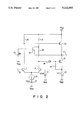
- FIG. 2 illustrates the circuit structure of the embodiment of the ECL circuit according to the present invention as applied to constitute an inverter circuit.
- a differential pair of NPN transistors 1 and 2 have their emitters commonly connected to a constant-current supply 3, which is connected to a constant-voltage supply 4.
- a constant-current supply 3 As the potential on the positive side (+) of the voltage supply 4 is connected to a ground voltage V SS , the current from the current supply 3 flows to a negative power supply voltage V EE on the negative side (-).
- An input terminal 5 is connected to the base of the transistor 1, while the ground voltage V SS is connected to the collector of the transistor 1. Between the collector of the transistor 1 and the ground voltage V SS is located a resistor 6.
- a constant-voltage supply 7 is connected between the base of the transistor 2 and the ground voltage V SS , and a predetermined reference voltage V ref whose value is between V SS and V EE is applied to the base of the transistor 2.
- the collector of the transistor 2 is also connected to the ground voltage V SS .
- resistors 8 and 9 are connected in a series.
- the collector of the transistor 1 is connected to the base of an output NPN transistor 10.
- the transistor 10 has its collector connected to the ground voltage V SS , and its emitter connected to an output terminal 11.
- An NPN transistor 12 has its collector connected to the contact point of the resistors 8 and 9 and its emitter connected to the output terminal 11.
- a constant-voltage supply 13 is inserted between the base of the transistor 12 and the ground voltage V SS , and a predetermined negative voltage V B whose value is between V SS and V EE is applied to the base of the transistor 12.
- a diode 14 has its anode connected to the collector of the transistor 2, and its cathode connected to the base of an NPN transistor 15.
- the collector of this transistor 15 is connected to the output terminal 11.
- the emitter and the base of the transistor 15 are connected to each other through a resistor 16.
- a constant-voltage supply 17 is arranged between the emitter of the transistor 15 and the ground voltage V SS , a predetermined negative voltage V TT whose value is between V SS and V EE is supplied to the emitter of the transistor 15.
- the transistor 1 When the signal of the input terminal 5 rises, the transistor 1 is switched on, and the collector potential of the transistor 2 rises. The current flows to the diode 14 in accordance with the collector potential, so that the transistor 15 is rendered on, reducing its collector potential. The potential of the output terminal 11, therefore, falls down to an "L" level (low level).
- the transistor 12, whose emitter is connected to the collector of the transistor 15, is turned on as the emitter potential decreases. Accordingly, the collector potential of the transistor 2 drops, thus decreasing the base potential of the transistor 15.
- the output terminal 11 is stably kept at the "L" level.
- a capacitor which interferes with integration is not used to drive the transistor 15 to lower the potential level of the output terminal 11, so that the circuit with the above structure is advantageous in realizing the integration.
- this circuit structure is most suitable for higher integration, because the collector current potential of the transistor 15 is used to lower the potential level of the output terminal 11 according to this embodiment, and the control circuit to control the collector current is so designed that the base current of the transistor 15 is controlled by the operation of a single transistor 12.
- the timings at which the transistor 12 is switched on and off are determined according to the divided resistance of the resistors 8 and 9, and the voltage V B of the voltage supply 13.
- the current flowing to the output terminal 11 is rapidly led toward the direction where it will be reduced, the potential of the output terminal 11 at this time is directly detected, and the transistor 15 is controlled through a feedback loop.
Landscapes
- Engineering & Computer Science (AREA)
- Physics & Mathematics (AREA)
- Computer Hardware Design (AREA)
- Computing Systems (AREA)
- General Engineering & Computer Science (AREA)
- Mathematical Physics (AREA)
- Power Engineering (AREA)
- Logic Circuits (AREA)
Applications Claiming Priority (2)
| Application Number | Priority Date | Filing Date | Title |
|---|---|---|---|
| JP2-21557 | 1990-01-31 | ||
| JP2021557A JPH0666679B2 (ja) | 1990-01-31 | 1990-01-31 | Ecl論理回路 |
Publications (1)
| Publication Number | Publication Date |
|---|---|
| US5122683A true US5122683A (en) | 1992-06-16 |
Family
ID=12058312
Family Applications (1)
| Application Number | Title | Priority Date | Filing Date |
|---|---|---|---|
| US07/646,207 Expired - Lifetime US5122683A (en) | 1990-01-31 | 1991-01-28 | Ecl circuit with feedback controlled pull down in output |
Country Status (5)
| Country | Link |
|---|---|
| US (1) | US5122683A (fr) |
| EP (1) | EP0440192B1 (fr) |
| JP (1) | JPH0666679B2 (fr) |
| KR (1) | KR930009152B1 (fr) |
| DE (1) | DE69118219T2 (fr) |
Cited By (6)
| Publication number | Priority date | Publication date | Assignee | Title |
|---|---|---|---|---|
| US5334886A (en) * | 1992-11-13 | 1994-08-02 | International Business Machines Corporation | Direct-coupled PNP transistor pull-up ECL circuits and direct-coupled complementary push-pull ECL circuits |
| EP0632595A1 (fr) * | 1993-06-28 | 1995-01-04 | Siemens Aktiengesellschaft | Circuit d'attaque de haute capacité dans une technique pour commutateurs |
| US5473272A (en) * | 1993-06-28 | 1995-12-05 | Siemens Aktiengesellschaft | Digital differential amplifier switching stage with current switch |
| US5736866A (en) * | 1995-11-13 | 1998-04-07 | Kabushiki Kaisha Toshiba | Active pull-down circuit for ECL using a capacitive coupled circuit |
| US6054874A (en) * | 1997-07-02 | 2000-04-25 | Cypress Semiconductor Corp. | Output driver circuit with switched current source |
| US6084439A (en) * | 1997-07-02 | 2000-07-04 | Cypress Semiconductor Corp. | Peak detector circuit with extended input voltage range |
Citations (9)
| Publication number | Priority date | Publication date | Assignee | Title |
|---|---|---|---|---|
| US4539493A (en) * | 1983-11-09 | 1985-09-03 | Advanced Micro Devices, Inc. | Dynamic ECL circuit adapted to drive loads having significant capacitance |
| US4629913A (en) * | 1982-05-10 | 1986-12-16 | Siemens Aktiengesellschaft | Circuit arrangement for converting ECL-logic signals to TTL-logic signals |
| US4687953A (en) * | 1986-04-18 | 1987-08-18 | Advanced Micro Devices, Inc. | Dynamic ECL line driver circuit |
| EP0314139A2 (fr) * | 1987-10-30 | 1989-05-03 | Nec Corporation | Convertisseur de niveau ECL-TTL |
| US4835420A (en) * | 1987-11-17 | 1989-05-30 | Applied Micro Circuits Corporation | Method and apparatus for signal level conversion with clamped capacitive bootstrap |
| EP0340725A2 (fr) * | 1988-05-02 | 1989-11-08 | Nec Corporation | Circuit de conversion de niveau ECL-TTL |
| US4948991A (en) * | 1988-11-03 | 1990-08-14 | Motorola Inc. | Load controlled ECL transient driver |
| US4970416A (en) * | 1988-09-30 | 1990-11-13 | Nec Corporation | Emitter coupled logic circuit having rapid output voltage |
| US5041743A (en) * | 1989-07-27 | 1991-08-20 | Nec Corporation | Emitter-follower circuit with reduced delay time |
Family Cites Families (2)
| Publication number | Priority date | Publication date | Assignee | Title |
|---|---|---|---|---|
| JPS60132037U (ja) * | 1984-02-15 | 1985-09-04 | 株式会社日立製作所 | 論理回路 |
| JPH0761000B2 (ja) * | 1984-03-28 | 1995-06-28 | 株式会社日立製作所 | 半導体集積回路 |
-
1990
- 1990-01-31 JP JP2021557A patent/JPH0666679B2/ja not_active Expired - Fee Related
-
1991
- 1991-01-18 KR KR1019910000771A patent/KR930009152B1/ko not_active Expired - Fee Related
- 1991-01-28 US US07/646,207 patent/US5122683A/en not_active Expired - Lifetime
- 1991-01-30 EP EP91101204A patent/EP0440192B1/fr not_active Expired - Lifetime
- 1991-01-30 DE DE69118219T patent/DE69118219T2/de not_active Expired - Fee Related
Patent Citations (9)
| Publication number | Priority date | Publication date | Assignee | Title |
|---|---|---|---|---|
| US4629913A (en) * | 1982-05-10 | 1986-12-16 | Siemens Aktiengesellschaft | Circuit arrangement for converting ECL-logic signals to TTL-logic signals |
| US4539493A (en) * | 1983-11-09 | 1985-09-03 | Advanced Micro Devices, Inc. | Dynamic ECL circuit adapted to drive loads having significant capacitance |
| US4687953A (en) * | 1986-04-18 | 1987-08-18 | Advanced Micro Devices, Inc. | Dynamic ECL line driver circuit |
| EP0314139A2 (fr) * | 1987-10-30 | 1989-05-03 | Nec Corporation | Convertisseur de niveau ECL-TTL |
| US4835420A (en) * | 1987-11-17 | 1989-05-30 | Applied Micro Circuits Corporation | Method and apparatus for signal level conversion with clamped capacitive bootstrap |
| EP0340725A2 (fr) * | 1988-05-02 | 1989-11-08 | Nec Corporation | Circuit de conversion de niveau ECL-TTL |
| US4970416A (en) * | 1988-09-30 | 1990-11-13 | Nec Corporation | Emitter coupled logic circuit having rapid output voltage |
| US4948991A (en) * | 1988-11-03 | 1990-08-14 | Motorola Inc. | Load controlled ECL transient driver |
| US5041743A (en) * | 1989-07-27 | 1991-08-20 | Nec Corporation | Emitter-follower circuit with reduced delay time |
Cited By (7)
| Publication number | Priority date | Publication date | Assignee | Title |
|---|---|---|---|---|
| US5334886A (en) * | 1992-11-13 | 1994-08-02 | International Business Machines Corporation | Direct-coupled PNP transistor pull-up ECL circuits and direct-coupled complementary push-pull ECL circuits |
| EP0632595A1 (fr) * | 1993-06-28 | 1995-01-04 | Siemens Aktiengesellschaft | Circuit d'attaque de haute capacité dans une technique pour commutateurs |
| US5473272A (en) * | 1993-06-28 | 1995-12-05 | Siemens Aktiengesellschaft | Digital differential amplifier switching stage with current switch |
| US5539350A (en) * | 1993-06-28 | 1996-07-23 | Siemens Aktiengesellschaft | Common mode logic line driver switching stage |
| US5736866A (en) * | 1995-11-13 | 1998-04-07 | Kabushiki Kaisha Toshiba | Active pull-down circuit for ECL using a capacitive coupled circuit |
| US6054874A (en) * | 1997-07-02 | 2000-04-25 | Cypress Semiconductor Corp. | Output driver circuit with switched current source |
| US6084439A (en) * | 1997-07-02 | 2000-07-04 | Cypress Semiconductor Corp. | Peak detector circuit with extended input voltage range |
Also Published As
| Publication number | Publication date |
|---|---|
| DE69118219T2 (de) | 1996-09-05 |
| EP0440192A1 (fr) | 1991-08-07 |
| JPH0666679B2 (ja) | 1994-08-24 |
| EP0440192B1 (fr) | 1996-03-27 |
| KR910015123A (ko) | 1991-08-31 |
| KR930009152B1 (ko) | 1993-09-23 |
| JPH03227119A (ja) | 1991-10-08 |
| DE69118219D1 (de) | 1996-05-02 |
Similar Documents
| Publication | Publication Date | Title |
|---|---|---|
| US4874970A (en) | ECL output with Darlington or common collector-common emitter drive | |
| US5122683A (en) | Ecl circuit with feedback controlled pull down in output | |
| JP2737444B2 (ja) | 高速論理回路 | |
| US4376252A (en) | Bootstrapped driver circuit | |
| US4236089A (en) | Floating power switch | |
| EP0098155B1 (fr) | Bascule de Schmitt | |
| US5258667A (en) | Logic circuit for controlling a supply on drive pulses to regulate an output level | |
| JPH0695611B2 (ja) | 開閉可能電流源回路 | |
| US4259599A (en) | Complementary transistor switching circuit | |
| US5120998A (en) | Source terminated transmission line driver | |
| EP0097248B1 (fr) | Source de courant commutable | |
| US4508979A (en) | Single-ended push-pull circuit having a small through-current | |
| JP2815434B2 (ja) | 出力回路装置 | |
| KR890004653B1 (ko) | 논리회로 | |
| US5087837A (en) | Electronic circuit with capacitively enhanced switching | |
| KR930010877B1 (ko) | 저전력소모용 발진회로 | |
| US4831344A (en) | IC output circuit for use in pulse width modulator | |
| US5616971A (en) | Power switching circuit | |
| US6262898B1 (en) | Circuit for driving a switching transistor | |
| JP2861356B2 (ja) | 半導体集積回路 | |
| JPH04315314A (ja) | 能動プルダウン回路 | |
| US4845442A (en) | High speed current limiting sense amplifier | |
| EP0055908B1 (fr) | Circuit logique bipolaire | |
| JP2570480B2 (ja) | レベル変換回路 | |
| JPH0730405A (ja) | Ecl回路 |
Legal Events
| Date | Code | Title | Description |
|---|---|---|---|
| AS | Assignment |
Owner name: KABUSHIKI KAISHA TOSHIBA, A CORP. OF JAPAN, JAPAN Free format text: ASSIGNMENT OF ASSIGNORS INTEREST.;ASSIGNORS:SUGOH, TAKESHI;SUGIMOTO, YASUHIRO;REEL/FRAME:005595/0077 Effective date: 19910116 |
|
| STCF | Information on status: patent grant |
Free format text: PATENTED CASE |
|
| FEPP | Fee payment procedure |
Free format text: PAYOR NUMBER ASSIGNED (ORIGINAL EVENT CODE: ASPN); ENTITY STATUS OF PATENT OWNER: LARGE ENTITY |
|
| FPAY | Fee payment |
Year of fee payment: 4 |
|
| FPAY | Fee payment |
Year of fee payment: 8 |
|
| FPAY | Fee payment |
Year of fee payment: 12 |