US5283095A - Optical recording medium comprising (1,1,1) aluminum - Google Patents
Optical recording medium comprising (1,1,1) aluminum Download PDFInfo
- Publication number
- US5283095A US5283095A US07/866,358 US86635892A US5283095A US 5283095 A US5283095 A US 5283095A US 86635892 A US86635892 A US 86635892A US 5283095 A US5283095 A US 5283095A
- Authority
- US
- United States
- Prior art keywords
- aluminum
- film
- ray
- aluminum film
- substrate
- Prior art date
- Legal status (The legal status is an assumption and is not a legal conclusion. Google has not performed a legal analysis and makes no representation as to the accuracy of the status listed.)
- Expired - Lifetime
Links
Images


Classifications
-
- C—CHEMISTRY; METALLURGY
- C23—COATING METALLIC MATERIAL; COATING MATERIAL WITH METALLIC MATERIAL; CHEMICAL SURFACE TREATMENT; DIFFUSION TREATMENT OF METALLIC MATERIAL; COATING BY VACUUM EVAPORATION, BY SPUTTERING, BY ION IMPLANTATION OR BY CHEMICAL VAPOUR DEPOSITION, IN GENERAL; INHIBITING CORROSION OF METALLIC MATERIAL OR INCRUSTATION IN GENERAL
- C23C—COATING METALLIC MATERIAL; COATING MATERIAL WITH METALLIC MATERIAL; SURFACE TREATMENT OF METALLIC MATERIAL BY DIFFUSION INTO THE SURFACE, BY CHEMICAL CONVERSION OR SUBSTITUTION; COATING BY VACUUM EVAPORATION, BY SPUTTERING, BY ION IMPLANTATION OR BY CHEMICAL VAPOUR DEPOSITION, IN GENERAL
- C23C18/00—Chemical coating by decomposition of either liquid compounds or solutions of the coating forming compounds, without leaving reaction products of surface material in the coating; Contact plating
- C23C18/16—Chemical coating by decomposition of either liquid compounds or solutions of the coating forming compounds, without leaving reaction products of surface material in the coating; Contact plating by reduction or substitution, e.g. electroless plating
-
- C—CHEMISTRY; METALLURGY
- C23—COATING METALLIC MATERIAL; COATING MATERIAL WITH METALLIC MATERIAL; CHEMICAL SURFACE TREATMENT; DIFFUSION TREATMENT OF METALLIC MATERIAL; COATING BY VACUUM EVAPORATION, BY SPUTTERING, BY ION IMPLANTATION OR BY CHEMICAL VAPOUR DEPOSITION, IN GENERAL; INHIBITING CORROSION OF METALLIC MATERIAL OR INCRUSTATION IN GENERAL
- C23C—COATING METALLIC MATERIAL; COATING MATERIAL WITH METALLIC MATERIAL; SURFACE TREATMENT OF METALLIC MATERIAL BY DIFFUSION INTO THE SURFACE, BY CHEMICAL CONVERSION OR SUBSTITUTION; COATING BY VACUUM EVAPORATION, BY SPUTTERING, BY ION IMPLANTATION OR BY CHEMICAL VAPOUR DEPOSITION, IN GENERAL
- C23C14/00—Coating by vacuum evaporation, by sputtering or by ion implantation of the coating forming material
- C23C14/06—Coating by vacuum evaporation, by sputtering or by ion implantation of the coating forming material characterised by the coating material
- C23C14/14—Metallic material, boron or silicon
- C23C14/20—Metallic material, boron or silicon on organic substrates
-
- Y—GENERAL TAGGING OF NEW TECHNOLOGICAL DEVELOPMENTS; GENERAL TAGGING OF CROSS-SECTIONAL TECHNOLOGIES SPANNING OVER SEVERAL SECTIONS OF THE IPC; TECHNICAL SUBJECTS COVERED BY FORMER USPC CROSS-REFERENCE ART COLLECTIONS [XRACs] AND DIGESTS
- Y10—TECHNICAL SUBJECTS COVERED BY FORMER USPC
- Y10S—TECHNICAL SUBJECTS COVERED BY FORMER USPC CROSS-REFERENCE ART COLLECTIONS [XRACs] AND DIGESTS
- Y10S428/00—Stock material or miscellaneous articles
- Y10S428/913—Material designed to be responsive to temperature, light, moisture
-
- Y—GENERAL TAGGING OF NEW TECHNOLOGICAL DEVELOPMENTS; GENERAL TAGGING OF CROSS-SECTIONAL TECHNOLOGIES SPANNING OVER SEVERAL SECTIONS OF THE IPC; TECHNICAL SUBJECTS COVERED BY FORMER USPC CROSS-REFERENCE ART COLLECTIONS [XRACs] AND DIGESTS
- Y10—TECHNICAL SUBJECTS COVERED BY FORMER USPC
- Y10T—TECHNICAL SUBJECTS COVERED BY FORMER US CLASSIFICATION
- Y10T428/00—Stock material or miscellaneous articles
- Y10T428/31504—Composite [nonstructural laminate]
- Y10T428/31678—Of metal
- Y10T428/31692—Next to addition polymer from unsaturated monomers
Definitions
- the present invention relates to a process for forming a metal film on a surface of a synthetic resin substrate and to an aluminum film coated matter formed by coating a surface of a synthetic resin substrate with an aluminum film.
- synthetic resin substrates such as acrylic resin moldings, provided with metal films formed on the respective surfaces thereof, are used in miscellaneous decoration goods, optical parts, optical recording media, etc.
- optical discs such as video discs for which the demand has increased remarkably in recent years, are provided by forming metal films such as aluminum films as reflection films on the respective surfaces of transparent synthetic resin substrates having recording pits corresponding to audio signals, video signals, etc.
- the metal films on this type substrates are heretofore formed mainly by a technique of vacuum evaporation.
- a technique of plasma sputtering parallel plate plasma sputtering
- the technique of vacuum evaporation is, in general, applied to an arrangement in which an evaporation source 8 and synthetic resin substrates 6 such as acrylic resin moldings opposite to the evaporation source 8 are provided in a vacuum vessel 2 as shown in FIG. 16, and it is a technique for respectively forming films of a metal such as aluminum on the respective surfaces of the substrates 6 by depositing particles 10 of a metal such as aluminum on the respective surfaces of the substrates 6 through evaporating the metal particles 10 from the evaporation source 8 by means of electron beam heating or resistance heating.
- the substrates 6 may be generally mounted on rotary holders 4 as shown in FIG. 16.
- a large number of substrates 6 may be arranged along the circumferential wall of a cylindrical vacuum vessel 2 having an evaporation source 11 in its center as shown in FIGS. 17 and 18.
- the evaporation source 11 has a large number of tungsten heaters 14 stretched between two props 12, and a large number of evaporation materials 16 such as aluminum attached thereto, so that the respective evaporation materials 16 are evaporated through heat generated by energizing the respective tungsten heaters 14.
- the reference numeral 18 designates a current input terminal.
- the substrates 6 are mounted on the holders 4 supported through rotary shafts 22 to holder supports 20, respectively, and they are rotated in the direction of the arrow A as shown in FIG. 17 in the vacuum vessel 2 as a whole.
- a sputtering source for example, magnetron type sputtering source
- a metal target 28 such as aluminum attached to the upper portion of a magnet 26 and synthetic resin substrates such as acrylic resin moldings opposite to the sputtering source 24 are provided in a vacuum vessel 2 as shown in FIG.
- metal reflection films of aluminum are most widely put into practical use in the field of optical discs such as video discs.
- the characteristic for example, S/N ratio
- the reflectivity of aluminum films formed on pits is determined by the reflectivity of aluminum films formed on pits as well as the form of the pits with respect to signal reproduction. In general, good images cannot be reproduced unless the reflectivity is not less than about 70%. Further, it is necessary in view of the producing process that the formed aluminum films sufficiently adhere to synthetic resin substrates.
- the technique of vacuum evaporation requires a large number of work steps because of problems on the lifetime of the resistors (for example, tungsten heaters 14 as shown in FIGS. 17 and 18) for resistance heating in the evaporation source, and on the supply of a metal such as aluminum being an evaporation material. Accordingly, a substantial problem against reduction in cost, that is, limitation in producing efficiency and stability of production, is inherent in the technique of vacuum evaporation.
- the resistors for example, tungsten heaters 14 as shown in FIGS. 17 and 18
- the technique of plasma sputtering a continuous operation can be made until the initially arranged metal target such as aluminum is worn out. This is effective for improvement in producing efficiency. Further, sufficient reflectivity can be obtained stably if the film thickness of metal films such as aluminum films is not less than 500 ⁇ .
- the technique of plasma sputtering has a problem in that the adhesion of metal films, especially, aluminum films, to synthetic resin substrates such as acrylic resin moldings is insufficient.
- the lowering of the adhesion of aluminum films is considered to be caused by resin surface deterioration, involving in resin injury due to temperature, produced by exposing surfaces of synthetic resin substrates to high-density plasma at the film-forming time and by some interaction between the aluminum films and impurity gas released from resin surfaces by heat due to inflow of acceleration electrons accelerated to high energy in an electric field, into the substrates as the anode side.
- the generally obtained performance thereof is heretofore limited to a range of about 72% to about 80% as its reflectivity and a range of about 38 dB to about 41 dB as S/N ratio of the regenerative output.
- high picture quality that is, in the case where, for example, the aluminum film is used for reproduction of high definition television images, there arises a problem in that the reproduced images are insufficient in sharpness if the reflectivity and S/N ratio is limited as described above.
- an aluminum film having higher reflectivity (80 to 85%) and higher S/N ratio (41 to 45 dB) can be provided by reducing the amount of oxidized aluminum in the aluminum film.
- the aluminum film thus provided has a tendency that there occurs easily a durability problem in that both rising of noise and lowering of recording strength are brought by corrosion and the like caused by moisture absorption oxidation and chemical reaction when the aluminum film is left for a long time. Accordingly, there arises a problem in that improvement in both the performance (reflectivity and S/N ratio) of the film and durability thereof cannot be attained simultaneously.
- a first object of the present invention is to provide a process for efficiently forming metal films being high in reflectivity and good in adhesion to synthetic resin substrates regardless of the reduction in film thickness of the metal films, thus to eliminate the aforementioned disadvantages from the two conventional techniques.
- a second object of the present invention is to provide an aluminum film coated matter having an aluminum film high in light reflectivity and excellent in durability.
- a first process metal film having a film thickness of 50 ⁇ to 400 ⁇ is formed on a surface of a synthetic resin substrate by sputtering a metal target through an inert gas ion beam in a vacuum atmosphere.
- a second process according to the present invention is characterized in that a film thickness of 50 ⁇ to 400 ⁇ is formed on a surface of a synthetic resin substrate by sputtering a metal target through ions in inert gas plasma in a vacuum atmosphere while using means for preventing diffusion of plasma to the surface of the synthetic resin substrate and for preventing inflow of acceleration electrons from the plasma to the surface of the synthetic resin substrate.
- the second object can be achieved by an aluminum film coated matter having an aluminum film as a constituent member of the aluminum film coated matter, in which: the aluminum film contains aluminum crystals at a portion in the film at a depth D of not more than 600 ⁇ from a film surface thereof which contacts with a substrate, the aluminum crystals having a relation in which a crystal axis ⁇ 111> perpendicular to a (111) plane is perpendicular or substantially perpendicular to the film surface.
- the second object can be achieved also by an aluminum film coated matter having an aluminum film as a constituent member of the aluminum film coated matter, in which: the aluminum film contains aluminum crystals at a portion in the film at a depth D of not more than 600 ⁇ from a film surface thereof which contacts with a substrate, the aluminum crystals exhibiting a diffraction X-ray spectrum of a (111) plane when measured by X-ray diffraction according to a diffractometer method under the following condition:
- incident height limiting slit 5 mm
- width limiting slit 5 mm
- the first process according to the present invention is called "ion beam sputtering".
- a surface of a metal target such as an aluminum target is beaten by an inert gas ion beam, so that metal particles flown out therefrom are deposited on the synthetic resin substrate such as an acrylic resin molding to thereby form a metal film on the synthetic resin substrate.
- the synthetic resin substrate such as an acrylic resin molding
- the second process according to the present invention technically belongs to the category of plasma sputtering.
- a surface of a metal target such as an aluminum target is beaten by ions in inert gas plasma, so that metal particles flown out therefrom are deposited on the synthetic resin substrate such as an acrylic resin molding to thereby form a metal film on the synthetic resin substrate.
- this lo film forming process is carried out while using means for preventing diffusion of plasma to the surface of the synthetic resin substrate and for preventing inflow of acceleration electrons from the plasma to the surface of the synthetic resin substrate. Accordingly, surface deterioration of the synthetic resin substrate and generation of an impurity gas as observed in the conventional technique of plasma sputtering can be prevented, so that a metal film high in adhesion can be formed.
- ions or ion beams used in the aforementioned process are ions or ion beams of inert gases such as argon gas, helium gas, neon gas, krypton gas, xenon gas, etc. If ions or ion beams of other gases such as nitrogen gas, oxygen gas, etc., are used, the reflectivity of metal films such as aluminum films may be lowered by interaction thereof with the metal films.
- Metal particles such as aluminum particles sputtered by this process have moderate kinetic energy of the order of several eV to about 20 eV. This energy contributes to improvement in the crystallization of the films, so that the metal films such as aluminum films accumulated on the synthetic resin substrates have a very fine structure, saying to be close-packed structure, and accordingly, the metal films are high in reflectivity even if the film thickness thereof is thin.
- metal films formed by the technique of ion beam sputtering or the like are so high in internal stress that a predetermined correlation may often occur between adhesion and film thickness. Therefore, both reflectivity and film thickness have been estimated about metal films having various film thicknesses. As a result, it has been found that metal films being good both in reflectivity and in adhesion can be formed when the film thickness thereof is in a range of 50 ⁇ to 400 ⁇ .
- the degree of vacuum in the atmosphere at the deposit time is preferably higher than about 4.0 ⁇ 10 -4 Torr.
- the energy of the ion beam is preferably higher than 100 eV which is a limit on sputtering. Generally, a range of about 200 eV to about 10 KeV can be used easily as the energy.
- the deposit rate is in a range of 1 ⁇ /sec to 500 ⁇ /sec when the energy of the ion beam is in the aforementioned range, the deposite rate is preferably lower than 200 to 400 ⁇ /sec in view of stability of production.
- Examples of the metal target used in the present invention include aluminum, platinum, gold, silver, chromium, and alloys thereof.
- the synthetic resin used in this invention is not limited specifically.
- the synthetic resin are acrylic resin, polystyrene, polycarbonate, polyolefin, modified epoxy resin, etc. These resins may be provided as homopolymers, copolymers or mixtures thereof.
- the aforementioned resins which are optical transparent resins used as optical disc substrate materials are preferably used in this invention.
- the acrylic resin used most preferably is not limited specifically.
- Preferred examples of the acrylic resin are resins high in transparency and excellent in other optical properties, such as methyl methacrylate polymer, methyl methacrylate-alkyl acrylate (C1 to C4) copolymer, methyl methacrylate-cyclohexyl methacrylate copolymer, methyl methacrylate-cyclohexylmethacrylate-bromhexylmethacrylatecopolymer, methacrylate-maleimide copolymer, methacrylatemethacrylimide copolymer, methacrylate-styrene copolymer, etc., and mixture resin compositions of these resins and synthetic transparent resins such as polycarbonate, etc.
- the shape of the synthetic resin substrates such as acrylic resin moldings is not limited specifically but preferred examples thereof are smooth shapes such as a disc shape, a plate shape, etc. Any suitable method selected from general methods such as a cast molding method, an injection molding method, a compression molding method, a laminating method, etc., can be employed as the method of forming the substrates.
- the aluminum film coated matter of the present invention was attained through the present inventors' investigation for the structure of an aluminum film formed on a substrate.
- the problem on reflectivity and durability of the conventional aluminum film coated matter is caused by the poor fineness and poor crystal arrangement of the aluminum film formed on a substrate. That is, the conventional aluminum film is porous (a polycrystalline substance not oriented). Accordingly, if the amount of oxidized alminum not contributing to light reflection is reduced by reducing the oxygen content of the film, the reflectivity of the film is improved but on the contrary the durability thereof is lowered because a tendency to increase the amount of water (or the like) penetrating into the film is brought by reduction of the amount of oxide for filling the porous portion.
- an arrangement in which the aluminum film contains aluminum crystals oriented preferentially in a direction effective for light reflection has an effect on achieving both high reflectivity and high durability. More specifically, light reflection is brought by interaction between incident light and aluminum atoms, so that higher reflectivity can be provided as the surface density of aluminum atoms in a surface perpendicular to the incident light increases. That is, aluminum has a plane-centered cubic lattice crystal structure, so that the (111) plane is a surface packing aluminum crystals at highest density.
- an aluminum film high in reflectivity can be provided by containing aluminum crystals preferentially oriented to the (111) plane and having the high-density packed surface of the crystal lattice in a section parallel or substantially parallel to the film surface, that is, by containing aluminum crystals having a relation in which a crystal axis ⁇ 111> perpendicular to the (111) plane is perpendicular or substantially perpendicular to the film surface as described above. This is particularly effective in the case where the incident light enters perpendicularly or substantially perpendicularly to the aluminum film surface.
- the aluminum film having such crystal orientation is also fine, so that penetration of water or the like can be prevented and, accordingly, the aluminum film is excellent in durability.
- a minimum value in the percentage distribution of the mole ratio (Al-O/Al) of oxidized alminum (Al-O) in a direction of the depth of the aluminum film to total aluminum (Al), measured by using an X-ray photoelectron spectroscopy is not more than 30%, more preferably, in a range of 10 to 25%.
- a film high in reflectivity can be provided by reducing the amount of oxidized alminum contained in the aluminum film.
- the film thickness of the aluminum film of the aluminum film coated matter is not limited specifically but it is generally set in a range of 50 to 600 ⁇ , preferably, in a range of 100 to 400 ⁇ under the consideration of producing efficiency and durability as well as reflectivity, because the portion not contributing to light reflection increases as the film thickness increases.
- the film thickness of the aluminum film is not more than 600 ⁇
- aluminum crystals having the aforementioned crystal orientation can be arranged at an arbitrary depth in the aluminum film.
- aluminum crystals can be arranged in the whole area in the aluminum film.
- Examples of the method for increasing the kinetic energy of aluminum particles deposited on the substrate include an ion beam sputtering technique, an evaporation technique using ion beam radiation, an ion beam depositing technique, an ion cluster beam technique, etc.
- the kinetic energy of deposited particles can be generally increased from the order of several eV to the order of hundreds of eV by using these techniques singly or in combination.
- the method used for forming the aluminum film coated matter according to this invention is not limited to specific one of the aforementioned techniques but the preferred example thereof is the ion beam sputtering technique by which the surface of the substrate made of a synthetic resin is free from damage due to plasma and heat.
- FIG. 1 is a schematic view showing an example of an ion beam sputtering apparatus for carrying out a metal film forming process according to the present invention
- FIG. 2 is a graph showing an example of the measurement result of the thickness-reflectivity characteristic of an aluminum film
- FIG. 3 is a schematic view showing an example of a plasma sputtering apparatus for carrying out a metal film forming process according to the present invention
- FIG. 4 is a schematic view showing another example of a plasma sputtering apparatus for carrying out a metal film forming process according to the present invention
- FIG. 5 is a sectional view schematically showing an example of an aluminum film coated matter according to the present invention.
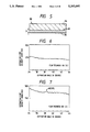
- FIG. 6 is a schematic graph showing an example of the result of the X-ray diffraction analysis of an aluminum film formed by the ion beam sputtering technique in the case where the thickness of the aluminum film is 100 ⁇ ;
- FIG. 7 is a schematic graph showing an example of the result of the X-ray diffraction analysis of an aluminum film formed by the ion beam sputtering technique in the case where the thickness of the aluminum film is 200 ⁇ ;
- FIG. 8 is a schematic graph showing an example of the result of the X-ray diffraction analysis of an aluminum film formed by the ion beam sputtering technique in the case where the thickness of the aluminum film is 300 ⁇ ;
- FIG. 9 is a schematic graph showing an example of the result of the X-ray diffraction analysis of an aluminum film formed by the ion beam sputtering technique in the case where the thickness of the aluminum film is 400 ⁇ ;
- FIG. 10 is a schematic graph showing an example of the result of the X-ray diffraction analysis of an aluminum film formed by the ion beam sputtering technique in the case where the thickness of the aluminum film is 500 ⁇ ;
- FIG. 11 is a schematic graph showing the relation between the thickness and the reflectivity of an aluminum film of Example 2 oriented in the (111) plane;
- FIG. 12 is a graph showing the relation between the diffraction X-ray spectrum intensity in the (111) plane and the reflectivity of an aluminum film;
- FIG. 13 is a schematic graph showing an example of the result of the X-ray diffraction analysis of an aluminum film formed by a conventional vacuum evaporation technique
- FIG. 14 is a schematic graph showing an example of the result of the X-ray diffraction analysis of an aluminum film formed by a conventional magnetron sputtering technique
- FIG. 15 is a graph showing the relation between the thickness and the reflectivity of an aluminum film formed by the conventional vacuum evaporation technique
- FIG. 16 is a schematic view showing an example of a conventional vacuum evaporation apparatus
- FIG. 17 is an upper view showing another example of a conventional vacuum evaporation apparatus
- FIG. 18 is a side view of the apparatus depicted in FIG. 17.
- FIG. 19 is a schematic view showing an example of a conventional plasma sputtering apparatus.
- FIG. 1 is a schematic view showing an example of an ion beam sputtering apparatus for carrying out a process for forming metal films according to the present invention.
- a holder 4 for holding an acrylic resin substrate 6a for an optical disc as an example of a synthetic resin substrate and a target holder 32 for holding an aluminum target 28a as an example of a metal target opposite to the acrylic resin substrate 6a are provided in a vacuum vessel 2.
- an ion source 34 is attached to the wall of the vacuum vessel 2 so as to be directed toward the aluminum target 28a on the target holder 32.
- the ion source 34 radiates an inert gas ion beam 36 of inert gas ions such as argon gas ions toward a surface of the aluminum target 28a to thereby sputter the aluminum target 28a.
- film forming was made as follows. That is, after an acrylic resin substrate 6a having a diameter of 300 mm was mounted on the holder 4 and the high-purity aluminum target 28a was mounted on the target 32, the vacuum vessel 2 was evacuated to 2.0 ⁇ 10 -5 Torr. The inert gas ion beam 36 was drawn out from the ion source 34 in the following condition and radiated toward a surface of the aluminum target 28a, so that aluminum particles 38 beaten out of the aluminum target 28a were deposited on a surface of the acrylic resin substrate 6a to thereby form an aluminum film on the acrylic resin substrate 6a. The thickness of the aluminum film was adjusted by the deposite time.
- FIG. 2 An example of the measurement result of the thickness-reflectivity characteristic of the aluminum film formed on the surface of the acrylic resin substrate 6a as described above is shown in FIG. 2. Although details of the result will be collectively shown in Table 1, reflectively of not less than 68% was obtained when the film thickness was not less than 50 ⁇ .
- the adhesion of the aluminum film to the acrylic resin substrate 6a was estimated by a tape peeling test in which an adhesive plane of a transparent adhesive tape was sufficiently pressed to a surface of the aluminum film and then rapidly vertically peeled from the surface. As a result, separation of the aluminum film was always observed when the film thickness was not less than 500 ⁇ ; separation of the aluminum film was sometimes observed when the film thickness was 400 ⁇ ; and separation of the aluminum film was not observed when the film thickness was less than 400 ⁇ .
- ⁇ represents “Excellent”
- ⁇ represents “Practicable” more or less inferior to “Excellent”
- x represents "Failure”.
- the wave length used for measuring reflectively was 780 nm which was the wave length of a semiconductor laser for optical discs.
- reflectivity of not less than about 70% can be secured when the thickness of the aluminum film is in a range of 50 ⁇ to 400 ⁇ , that is, when the film thickness is not more than two thirds the film thickness in the conventional technique of vacuum evaporation. Further, more excellent adhesion than that in the conventional technique of plasma sputtering can be obtained.
- film forming may be applied to a plurality of acrylic resin substrates at once. Further, in this case, the respective acrylic resin substrates may be rotated to make aluminum thin films even.
- IBS represents an ion beam sputtering technique
- PS represents a conventional plasma sputtering technique
- EB represents a conventional vacuum evaporation technique.
- the wave length used for measuring reflectivity was 780 nm which was the same as described above.
- the gold, silver and copper films formed by the process according to the present invention are so excellent both in reflectivity and in adhesion as to be adapted for optical discs, and that the platinum film is more or less inferior but practicable in reflectivity and is excellent in adhesion.
- the gold, silver and platinum films formed by the conventional vacuum evaporation technique may be said to be practicable in adhesion but cannot be said to be practicable in reflectivity as adapted for optical discs because the films are so thin that the reflectivity thereof becomes bad.
- the metal films formed by the conventional plasma sputtering technique are bad in adhesion.
- FIGS. 3 and 4 Examples of plasma sputtering apparatus having means of preventing diffusion of plasma to surfaces of synthetic resin substrates and preventing inflow of acceleration electrons to the surfaces of the substrates are shown in FIGS. 3 and 4.
- the apparatus shown in FIG. 3 uses opposed target sputtering technique.
- two metal targets 28 are arranged in a vacuum vessel 2 so as to be opposite to each other.
- Magnets 40 different in polarity are arranged in the back of the metal targets 28, respectively.
- the reference numeral 42 designates holders.
- a plurality of synthetic resin substrates 6 mounted on the holders 4 are arranged around the opposite metal targets 28.
- the reference numeral 52 designates supports for holders.
- cylindrical anodes 46 are arranged around the metal targets 28, respectively.
- the reference numeral 44 designates electrical insulating substances.
- high-density inert gas plasma 30a is generated between the two metal targets 28 by an electric field formed between the anodes 46 and the metal targets 28 and a magnetic field (the reference numeral 48 designates magnetic force lines as a typical example) formed between the opposite metal targets 28, when an inert gas is introduced in the vacuum vessel 2 to form moderate pressure and at the same time a voltage is applied between the anodes 46 and the metal targets 28.
- the inert gas plasma 30a is enclosed in a space by the magnetic field formed between the opposite metal targets 28 but acceleration electrons trying to go out of the inert gas plasma 30a are enclosed in the same space by the magnetic field in the same manner as described above. Accordingly, damage given to surfaces of the synthetic resin substrates 6 by the plasma and the acceleration electrons can be prevented.
- the apparatus shown in FIG. 4 basically uses the same magnetron sputtering technique as used in the apparatus shown in FIG. 19.
- a mesh-like electrostatic shield 54 of not lower in electric potential than the holders 4 is arranged so that the neighborhood of the surfaces of the synthetic resin substrates 6 mounted on the holders 4 can be covered at the least.
- inert gas plasma 30a is generated between the electrostatic shield 54 and the sputtering source 24 and at the same time there is no electric field generated between the electrostatic shield 54 and the holders 4 or, if there lo is any electric field, the electric field serves to press the inert gas plasma 30a back. Accordingly, the inert gas plasma 30a cannot pass through the electrostatic shield 54, so that the inert gas plasma 30a cannot be diffused to the side of the synthetic resin substrates 6. Further, acceleration electrons from the inert gas plasma 30a cannot flow in the electrostatic shield 54, so that the acceleration electrons cannot reach the synthetic resin substrates 6. Accordingly, damage given to the surfaces of the synthetic resin substrates 6 by the plasma and the acceleration electrons can be prevented.
- the excellent characteristic of metal films formed on surfaces of synthetic resin substrates by the aforementioned processes according to the present invention can be widely used for other purposes than the purpose for optical discs.
- the metal films can be used as metal reflection films in miscellaneous decoration goods, optical parts, etc.
- metal films high in reflectivity and excellent in adhesion to synthetic resin substrates can be formed even in the case where the metal films are sufficiently thin.
- material saving and shortening of deposite time can be attained, so that an improvement in producing efficiency can be attained.
- reduction in cost of optical discs Or the like can be attained.
- the processes according to the present invention technically belongs to the category of sputtering, so that, unlike the vacuum evaporation technique, the film forming processes can be continued before the initially arranged metal target is worn out. Accordingly, metal films can be formed efficiently, so that improvement in producing efficiency can be also attained in this sense.
- an aluminum film 66 of an aluminum film coated matter 62 contains aluminum crystals at a portion in the film at a depth D of not more than 600 ⁇ from a film surface 65 thereof which contacts with a substrate 64, the aluminum crystals having a relation in which a crystal axis ⁇ 111> perpendicular to a (111) plane is perpendicular or substantially perpendicular to the film surface 65.
- the aluminum film 66 contains aluminum crystals at a portion in the film at a depth D of not more than 600 ⁇ from the film surface 65 thereof which contacts with the substrate 64, the aluminum crystals exhibiting a diffraction X-ray spectrum of a (111) plane when measured by X-ray diffraction according to a diffractometer method under the following condition:
- incident height limiting slit 5 mm
- width limiting slit 5 mm
- film forming was made as follows. That is, after an acrylic resin substrate 6a having a diameter of 300 mm as an example of the substrate 64 made of a synthetic resin (see FIG. 5) was mounted to a holder 4 and a high-purity aluminum target 28a was mounted to a target holder 32, the vacuum vessel 2 was evacuated to 2.0 ⁇ 10 -7 Torr.
- An inert gas ion beam 36 was drawn out from the ion source 34 in the following condition and radiated toward a surface of the aluminum target 28a, so that aluminum particles 38 sputtered out of the aluminum target 28a were deposited on a surface of the acrylic resin substrate 6a, thus to form an aluminum film on the acrylic resin substrate 6a.
- the thickness of the aluminum film was adjusted by the deposite time.
- Aluminum films respectively having film thicknesses of 100 ⁇ , 200 ⁇ , 300 ⁇ , 400 ⁇ and 500 ⁇ were formed on acrylic resin substrates 6a in the same manner as described above by the ion beam sputtering technique and then subjected to X-ray diffraction analysis. The results of the analysis are shown in FIGS. 6 through 10. As shown in FIGS. 7 through 10, the clear crystal orientation of aluminum in the (111) plane was confirmed when the film thickness was not less than 200 ⁇ . It was found from this fact that the aluminum film formed by the aforementioned technique, especially, the aluminum film having a thickness of not less than 200 ⁇ , is a film high in the surface density of aluminum atoms.
- Measuring Apparatus X-ray diffraction apparatus RAD-2B made by RIGAKU Co., Ltd.
- Width Limiting Slit 5 mm
- Measuring Apparatus X-ray diffraction apparatus RAD-2B made by RIGAKU Co., Ltd.
- Width Limiting Slit 5 mm
- a video disc was produced by using the matter Obtained by the aforementioned process and was subjected to an acceleration deterioration test in a constant-temperature constant-humidity condition of 60° C. and 60%. As a result, deterioration of reproduced images was not observed at all even after the passage of 2000 hours.
- Aluminum films with the thicknesses of 2000 ⁇ and 3000 ⁇ were respectively formed on acrylic resin substrates by the vacuum evaporation technique and the plasma sputtering technique (magnetron sputtering technique) and subjected to X-ray diffraction analysis.
- the vacuum evaporation technique and the plasma sputtering technique magnetic sputtering technique
- X-ray diffraction analysis As a result, no peak (diffraction X-ray spectrum) except the noise level was observed as shown in FIGS. 13 and 14 in the following X-ray diffraction condition when the diffraction angle 2 ⁇ was in a range of 20 degrees to 80 degrees. It is apparent from the result that the aluminum films formed by the conventional techniques have a non-oriented crystal structure.
- Measuring Apparatus X-ray diffraction apparatus RAD-2B made by RIGAKU Co., Ltd.
- Width Limiting Slit 5 mm
- the oxygen content (in the more strict sense, the oxidized alminum content) in each of the aluminum films formed in Examples 2 and 4 and Comparative Examples 3 and 4 was analyzed by X-ray photoelectron spectroscopy (XPS). Specifically, analysis was made in respective layers in the following measurement condition while 30 times-50 times repeating argon ion beam etching (condition: ion beam energy 2 KeV, beam current 20 mA, the degree of vacuum 3.8 ⁇ 10 -6 Torr) were conducted from the aluminum film surface toward the substrate until carbon (C) contained in the substrate became a main component, by using an X-ray photoelectron spectrometer ESCA-750 made by Shimadzu Seisakusho Ltd.
- XPS X-ray photoelectron spectroscopy
- the thus obtained Al 2P1/2 and Al 2P3/2 spectra of the respective layers exhibit a mixture state of oxidized alminum (Al-O) and metal aluminum (Al). Therefore, after the respective spectra were separated into an oxidized alminum peak and a metal aluminum peak, the area ratio (that is, mole ratio (Al-O/Al) of oxidized alminum (Al-O) to total aluminum (Al) was calculated. Then, a graph was obtained through plotting the area ratio in a direction of the depth of the film. Since the graph is normally a concave curve having high values at both surfaces of the film and low values at the inside of the film, the lowest value of the curve was defined as the minimum value.
- the minimum value is normally proportional to the amount of the oxidized aluminum (Al-O).
- Al-O oxidized aluminum
- the characteristics, inclusive of durability, of the aluminum films obtained in Example 2 and Comparative Examples 3 and 4 in the two cases of the thickness of 300 ⁇ and the thickness of 600 ⁇ are collectively shown in Table 3.
- the reflectivity in each of the aluminum films is the same as shown in FIGS. 11 and 15.
- the durability in each of the aluminum was estimated on the basis of deterioration of reproduced images by applying an acceleration deterioration test to a video disc having an aluminum film formed in the same condition as in each example after putting the video disc into a constant-temperature constant-humidity tank of 60° C. and 60%.
- the alruainum film in Example 2 exhibits high reflectivity and good durability in either film thickness.
- the aluminum film in Comparative Example 3 is good in durability but low in reflectivity, because the oxidized alminum content thereof is large.
- the aluminum film in Comparative Example 4 is considerably high in reflectivity but poor in durability, because the oxidized alminum content thereof is small.
- the aluminum film coated matter according to this invention is adapted to optical information recording media such as video discs, compact discs, compact disc read only memories (CD-ROM), write once (WO) discs, and rewritable (RW) discs, but it is adapted to goods particularly requiring high reflectivity and durability, such as optical parts, miscellaneous decoration goods, etc.
- the aluminum film coated matter according to this invention contains aluminum crystals oriented as described above in the film, so that the film is high in light reflectivity and excellent in durability. Accordingly, when, for example, the aluminum film coated matter is used as an optical information recording medium, not only improvement both in reflectivity and in S/N ratio can be attained but improvement in durability can be attained.
Landscapes
- Chemical & Material Sciences (AREA)
- Chemical Kinetics & Catalysis (AREA)
- Engineering & Computer Science (AREA)
- Materials Engineering (AREA)
- Mechanical Engineering (AREA)
- Metallurgy (AREA)
- Organic Chemistry (AREA)
- General Chemical & Material Sciences (AREA)
- Physical Vapour Deposition (AREA)
- Chemically Coating (AREA)
- Manufacturing Optical Record Carriers (AREA)
- Optical Record Carriers And Manufacture Thereof (AREA)
Priority Applications (1)
| Application Number | Priority Date | Filing Date | Title |
|---|---|---|---|
| US08/130,199 US5431794A (en) | 1991-04-12 | 1993-11-05 | Process for forming metal films by plasma sputtering |
Applications Claiming Priority (4)
| Application Number | Priority Date | Filing Date | Title |
|---|---|---|---|
| JP10878591A JPH04314860A (ja) | 1991-04-12 | 1991-04-12 | 金属膜の形成方法 |
| JP3-108785 | 1991-04-12 | ||
| JP02611592A JP3255682B2 (ja) | 1992-01-16 | 1992-01-16 | アルミニウム膜被着物 |
| JP4-026115 | 1992-01-16 |
Related Child Applications (1)
| Application Number | Title | Priority Date | Filing Date |
|---|---|---|---|
| US08/130,199 Division US5431794A (en) | 1991-04-12 | 1993-11-05 | Process for forming metal films by plasma sputtering |
Publications (1)
| Publication Number | Publication Date |
|---|---|
| US5283095A true US5283095A (en) | 1994-02-01 |
Family
ID=26363851
Family Applications (2)
| Application Number | Title | Priority Date | Filing Date |
|---|---|---|---|
| US07/866,358 Expired - Lifetime US5283095A (en) | 1991-04-12 | 1992-04-10 | Optical recording medium comprising (1,1,1) aluminum |
| US08/130,199 Expired - Lifetime US5431794A (en) | 1991-04-12 | 1993-11-05 | Process for forming metal films by plasma sputtering |
Family Applications After (1)
| Application Number | Title | Priority Date | Filing Date |
|---|---|---|---|
| US08/130,199 Expired - Lifetime US5431794A (en) | 1991-04-12 | 1993-11-05 | Process for forming metal films by plasma sputtering |
Country Status (9)
| Country | Link |
|---|---|
| US (2) | US5283095A (fr) |
| EP (1) | EP0508478B1 (fr) |
| KR (1) | KR100237085B1 (fr) |
| AT (1) | ATE140040T1 (fr) |
| AU (3) | AU652039B2 (fr) |
| CA (1) | CA2065833C (fr) |
| DE (1) | DE69211885T2 (fr) |
| SG (1) | SG44529A1 (fr) |
| TW (1) | TW198069B (fr) |
Cited By (3)
| Publication number | Priority date | Publication date | Assignee | Title |
|---|---|---|---|---|
| US6461705B2 (en) * | 2000-02-24 | 2002-10-08 | Glass Unlimited Of High Point, Inc. | Glass panel with simulated metal strip |
| US20070269670A1 (en) * | 2006-05-17 | 2007-11-22 | Ronald Wilmer | Multilayered structures and their use as optical storage media |
| CN115542952A (zh) * | 2022-11-30 | 2022-12-30 | 昆明理工大学 | 一种面向无人机集群智能协同系统的优化方法 |
Families Citing this family (12)
| Publication number | Priority date | Publication date | Assignee | Title |
|---|---|---|---|---|
| US6162495A (en) * | 1997-09-29 | 2000-12-19 | Cymer, Inc. | Protective overcoat for replicated diffraction gratings |
| US6330261B1 (en) | 1997-07-18 | 2001-12-11 | Cymer, Inc. | Reliable, modular, production quality narrow-band high rep rate ArF excimer laser |
| US6511703B2 (en) * | 1997-09-29 | 2003-01-28 | Cymer, Inc. | Protective overcoat for replicated diffraction gratings |
| US6121134A (en) | 1998-04-21 | 2000-09-19 | Micron Technology, Inc. | High aspect ratio metallization structures and processes for fabricating the same |
| US6320261B1 (en) | 1998-04-21 | 2001-11-20 | Micron Technology, Inc. | High aspect ratio metallization structures for shallow junction devices, and methods of forming the same |
| EP1139340B1 (fr) * | 2000-03-29 | 2004-06-16 | TDK Corporation | Support d'enregistrement optique comportant une couche réfléchissante d'argent orienté |
| KR100425453B1 (ko) * | 2001-07-06 | 2004-03-30 | 삼성전자주식회사 | 고밀도 플라즈마용 자석과 그 제조방법 및 이를 이용한고밀도 플라즈마용 반도체 제조장치 |
| US20040055871A1 (en) * | 2002-09-25 | 2004-03-25 | The Regents Of The University Of California | Use of ion beams for protecting substrates from particulate defect contamination in ultra-low-defect coating processes |
| US20050150758A1 (en) * | 2004-01-09 | 2005-07-14 | Yakshin Andrey E. | Processes and device for the deposition of films on substrates |
| US7700167B2 (en) * | 2006-08-31 | 2010-04-20 | Honeywell International Inc. | Erosion-protective coatings on polymer-matrix composites and components incorporating such coated composites |
| US8691064B2 (en) * | 2007-07-09 | 2014-04-08 | Raytheon Canada Limited | Sputter-enhanced evaporative deposition apparatus and method |
| CN106282955A (zh) * | 2016-08-31 | 2017-01-04 | 北京埃德万斯离子束技术研究所股份有限公司 | 一种在柔性基底薄膜上制备功能性图形薄膜的方法 |
Citations (11)
| Publication number | Priority date | Publication date | Assignee | Title |
|---|---|---|---|---|
| US4426275A (en) * | 1981-11-27 | 1984-01-17 | Deposition Technology, Inc. | Sputtering device adaptable for coating heat-sensitive substrates |
| JPS59116376A (ja) * | 1982-12-22 | 1984-07-05 | Teijin Ltd | 対向タ−ゲツト式スパツタ装置 |
| US4692402A (en) * | 1986-02-20 | 1987-09-08 | Drexler Technology Corporation | Ultrathin optical recording medium with moisture barrier |
| EP0269111A2 (fr) * | 1986-11-27 | 1988-06-01 | Nissin Electric Company, Limited | Procédé de formation d'un film mince en aluminium |
| JPS63166963A (ja) * | 1986-12-27 | 1988-07-11 | Nissin Electric Co Ltd | 薄膜の製造方法 |
| US4767661A (en) * | 1986-09-15 | 1988-08-30 | Psi Star | Copper etching process and product |
| EP0316004A2 (fr) * | 1987-11-11 | 1989-05-17 | Kabushiki Kaisha Toshiba | Disque optique et procédé pour sa fabrication |
| US4983440A (en) * | 1987-05-30 | 1991-01-08 | Kuraray Company, Ltd. | Optical recording medium and recording process utilizing the same |
| EP0422323A1 (fr) * | 1989-10-12 | 1991-04-17 | Leybold Aktiengesellschaft | Utilisation d'helium comme gaz pour revêtir un substrat de polyméthylméthacrylate avec une couche mince de l'aluminium |
| US5075145A (en) * | 1989-04-07 | 1991-12-24 | Fuji Photo Film Co., Ltd. | Optical recording medium |
| US5147726A (en) * | 1988-09-28 | 1992-09-15 | Toray Industries, Inc. | Aluminum deposited film and process for producing it |
Family Cites Families (6)
| Publication number | Priority date | Publication date | Assignee | Title |
|---|---|---|---|---|
| JPS59116374A (ja) * | 1982-12-23 | 1984-07-05 | Sony Corp | 蒸着装置 |
| JPS59203994A (ja) * | 1983-05-06 | 1984-11-19 | 株式会社日立製作所 | 沸騰水型原子炉の水位計測装置 |
| JPS63270461A (ja) * | 1986-12-26 | 1988-11-08 | Teijin Ltd | 対向ターゲット式スパッタ装置 |
| JP2610133B2 (ja) * | 1987-07-23 | 1997-05-14 | 国際電信電話株式会社 | 双方向光増幅器を用いた多地点間光増幅中継装置 |
| EP0383301B1 (fr) * | 1989-02-15 | 1999-09-15 | Hitachi, Ltd. | Procédé et appareillage de formation d'un film |
| JPH02217467A (ja) * | 1989-02-17 | 1990-08-30 | Pioneer Electron Corp | 対向ターゲット型スパッタリング装置 |
-
1992
- 1992-04-10 AU AU14857/92A patent/AU652039B2/en not_active Ceased
- 1992-04-10 SG SG1996001567A patent/SG44529A1/en unknown
- 1992-04-10 US US07/866,358 patent/US5283095A/en not_active Expired - Lifetime
- 1992-04-10 KR KR1019920005941A patent/KR100237085B1/ko not_active Expired - Fee Related
- 1992-04-10 EP EP19920106293 patent/EP0508478B1/fr not_active Expired - Lifetime
- 1992-04-10 AT AT92106293T patent/ATE140040T1/de not_active IP Right Cessation
- 1992-04-10 CA CA 2065833 patent/CA2065833C/fr not_active Expired - Fee Related
- 1992-04-10 DE DE69211885T patent/DE69211885T2/de not_active Expired - Fee Related
- 1992-04-11 TW TW81102874A patent/TW198069B/zh active
-
1993
- 1993-11-05 US US08/130,199 patent/US5431794A/en not_active Expired - Lifetime
-
1994
- 1994-04-19 AU AU60570/94A patent/AU659594B2/en not_active Ceased
- 1994-04-19 AU AU60569/94A patent/AU6056994A/en not_active Abandoned
Patent Citations (12)
| Publication number | Priority date | Publication date | Assignee | Title |
|---|---|---|---|---|
| US4426275A (en) * | 1981-11-27 | 1984-01-17 | Deposition Technology, Inc. | Sputtering device adaptable for coating heat-sensitive substrates |
| JPS59116376A (ja) * | 1982-12-22 | 1984-07-05 | Teijin Ltd | 対向タ−ゲツト式スパツタ装置 |
| US4692402A (en) * | 1986-02-20 | 1987-09-08 | Drexler Technology Corporation | Ultrathin optical recording medium with moisture barrier |
| US4767661A (en) * | 1986-09-15 | 1988-08-30 | Psi Star | Copper etching process and product |
| EP0269111A2 (fr) * | 1986-11-27 | 1988-06-01 | Nissin Electric Company, Limited | Procédé de formation d'un film mince en aluminium |
| JPS63166963A (ja) * | 1986-12-27 | 1988-07-11 | Nissin Electric Co Ltd | 薄膜の製造方法 |
| US4983440A (en) * | 1987-05-30 | 1991-01-08 | Kuraray Company, Ltd. | Optical recording medium and recording process utilizing the same |
| EP0316004A2 (fr) * | 1987-11-11 | 1989-05-17 | Kabushiki Kaisha Toshiba | Disque optique et procédé pour sa fabrication |
| US5147726A (en) * | 1988-09-28 | 1992-09-15 | Toray Industries, Inc. | Aluminum deposited film and process for producing it |
| US5075145A (en) * | 1989-04-07 | 1991-12-24 | Fuji Photo Film Co., Ltd. | Optical recording medium |
| EP0422323A1 (fr) * | 1989-10-12 | 1991-04-17 | Leybold Aktiengesellschaft | Utilisation d'helium comme gaz pour revêtir un substrat de polyméthylméthacrylate avec une couche mince de l'aluminium |
| US5074984A (en) * | 1989-10-12 | 1991-12-24 | Leybold Aktiengesellschaft | Method for coating polymethylmethacrylate substrate with aluminum |
Non-Patent Citations (4)
| Title |
|---|
| Australian Office Action, dated Jul. 22, 1993. * |
| Copy of the European Search Report dated Jul. 28, 1992. * |
| Y. Suzuki et al, "Preparation of CoCr thin films on polymer substrates by ion beam sputtering," J. Vac. Sci. Technol. 5(4), Jul./Aug. 1987, pp. 1870-1873. |
| Y. Suzuki et al, Preparation of CoCr thin films on polymer substrates by ion beam sputtering, J. Vac. Sci. Technol. 5(4), Jul./Aug. 1987, pp. 1870 1873. * |
Cited By (6)
| Publication number | Priority date | Publication date | Assignee | Title |
|---|---|---|---|---|
| US6461705B2 (en) * | 2000-02-24 | 2002-10-08 | Glass Unlimited Of High Point, Inc. | Glass panel with simulated metal strip |
| US6524674B1 (en) * | 2000-02-24 | 2003-02-25 | Glass Unlimited Of High Point, Inc. | Glass panel with simulated metal strip |
| US6752891B2 (en) * | 2000-02-24 | 2004-06-22 | Glass Unlimited Of High Point, Inc. | Glass panel with simulated metal strip |
| US20070269670A1 (en) * | 2006-05-17 | 2007-11-22 | Ronald Wilmer | Multilayered structures and their use as optical storage media |
| CN115542952A (zh) * | 2022-11-30 | 2022-12-30 | 昆明理工大学 | 一种面向无人机集群智能协同系统的优化方法 |
| CN115542952B (zh) * | 2022-11-30 | 2023-03-03 | 昆明理工大学 | 一种面向无人机集群智能协同系统的优化方法 |
Also Published As
| Publication number | Publication date |
|---|---|
| KR100237085B1 (ko) | 2000-01-15 |
| DE69211885T2 (de) | 1996-10-31 |
| TW198069B (fr) | 1993-01-11 |
| US5431794A (en) | 1995-07-11 |
| AU652039B2 (en) | 1994-08-11 |
| CA2065833C (fr) | 1997-12-30 |
| AU1485792A (en) | 1992-10-15 |
| ATE140040T1 (de) | 1996-07-15 |
| AU659594B2 (en) | 1995-05-18 |
| CA2065833A1 (fr) | 1992-10-13 |
| EP0508478B1 (fr) | 1996-07-03 |
| AU6057094A (en) | 1994-06-23 |
| KR920019964A (ko) | 1992-11-20 |
| EP0508478A1 (fr) | 1992-10-14 |
| DE69211885D1 (de) | 1996-08-08 |
| SG44529A1 (en) | 1997-12-19 |
| AU6056994A (en) | 1994-06-16 |
Similar Documents
| Publication | Publication Date | Title |
|---|---|---|
| US5283095A (en) | Optical recording medium comprising (1,1,1) aluminum | |
| US4287225A (en) | Process of making a magnetic recording medium | |
| US4387136A (en) | Magnetic recording medium and apparatus for preparing the same | |
| US4426265A (en) | Method of producing a metallic thin film magnetic disk | |
| US5589040A (en) | Process for producing optical recording medium sputtering method and sputtering target | |
| US4839207A (en) | Optical recording medium and process for producing the same | |
| US4002546A (en) | Method for producing a magnetic recording medium | |
| CA2199424C (fr) | Procede de formation d'un film de metal sur la surface d'un substrat de resine synthetique | |
| JP3255682B2 (ja) | アルミニウム膜被着物 | |
| JPS61235560A (ja) | マグネトロンスパツタ装置 | |
| EP0335275A2 (fr) | Support d'enregistrement d'information | |
| JPH0444812B2 (fr) | ||
| JPS641851B2 (fr) | ||
| JPS60124290A (ja) | 光学記録媒体の製造方法 | |
| JPH0551739A (ja) | 光磁気デイスクの製造方法 | |
| JPH04314860A (ja) | 金属膜の形成方法 | |
| JP2703359B2 (ja) | 磁気記録媒体及びその製造方法 | |
| JPH0793807A (ja) | 情報記録媒体およびその製造方法 | |
| Jhingan et al. | Film growth characterization of an underlayer for perpendicular magnetic recording | |
| JPS6157028A (ja) | 垂直磁気記録媒体 | |
| JPS62229550A (ja) | 光デイスクの製造方法及び製造装置 | |
| JPS62148291A (ja) | 光学式情報記録担体およびその製造方法 | |
| JPS59198543A (ja) | 光記録用媒体とその作製方法 | |
| JPH02169293A (ja) | 情報記録媒体 | |
| JPH02169294A (ja) | 情報記録媒体 |
Legal Events
| Date | Code | Title | Description |
|---|---|---|---|
| AS | Assignment |
Owner name: NISSIN ELECTRIC CO., LTD., A CORPORATION OF JAPAN, Free format text: ASSIGNMENT OF ASSIGNORS INTEREST.;ASSIGNORS:MATSUMARU, SHIGEO;WATANABE, TORU;KUBOTSU, AKIRA;AND OTHERS;REEL/FRAME:006086/0741 Effective date: 19920406 Owner name: KURARAY CO., LTD., A CORPORATION OF JAPAN, JAPAN Free format text: ASSIGNMENT OF ASSIGNORS INTEREST.;ASSIGNORS:MATSUMARU, SHIGEO;WATANABE, TORU;KUBOTSU, AKIRA;AND OTHERS;REEL/FRAME:006086/0741 Effective date: 19920406 |
|
| STCF | Information on status: patent grant |
Free format text: PATENTED CASE |
|
| CC | Certificate of correction | ||
| FPAY | Fee payment |
Year of fee payment: 4 |
|
| FEPP | Fee payment procedure |
Free format text: PAYOR NUMBER ASSIGNED (ORIGINAL EVENT CODE: ASPN); ENTITY STATUS OF PATENT OWNER: LARGE ENTITY |
|
| FPAY | Fee payment |
Year of fee payment: 8 |
|
| FPAY | Fee payment |
Year of fee payment: 12 |