US5438531A - Zero dead time acquisition for a digital storage oscilloscope - Google Patents
Zero dead time acquisition for a digital storage oscilloscope Download PDFInfo
- Publication number
- US5438531A US5438531A US08/085,368 US8536893A US5438531A US 5438531 A US5438531 A US 5438531A US 8536893 A US8536893 A US 8536893A US 5438531 A US5438531 A US 5438531A
- Authority
- US
- United States
- Prior art keywords
- sample
- acquisition
- data samples
- digital data
- samples
- Prior art date
- Legal status (The legal status is an assumption and is not a legal conclusion. Google has not performed a legal analysis and makes no representation as to the accuracy of the status listed.)
- Expired - Lifetime
Links
- 230000015654 memory Effects 0.000 claims abstract description 72
- 238000009825 accumulation Methods 0.000 claims abstract description 14
- 239000000523 sample Substances 0.000 claims description 103
- 238000000034 method Methods 0.000 claims description 13
- 239000013074 reference sample Substances 0.000 claims description 10
- 230000004044 response Effects 0.000 claims description 3
- 239000000872 buffer Substances 0.000 abstract description 23
- 230000008569 process Effects 0.000 description 6
- 238000010586 diagram Methods 0.000 description 3
- 238000010894 electron beam technology Methods 0.000 description 3
- 101100129496 Arabidopsis thaliana CYP711A1 gene Proteins 0.000 description 1
- 101100083446 Danio rerio plekhh1 gene Proteins 0.000 description 1
- 230000008859 change Effects 0.000 description 1
- 238000006243 chemical reaction Methods 0.000 description 1
- 230000003111 delayed effect Effects 0.000 description 1
- 230000006870 function Effects 0.000 description 1
- 230000003252 repetitive effect Effects 0.000 description 1
- 238000005070 sampling Methods 0.000 description 1
Images


Classifications
-
- G—PHYSICS
- G01—MEASURING; TESTING
- G01R—MEASURING ELECTRIC VARIABLES; MEASURING MAGNETIC VARIABLES
- G01R13/00—Arrangements for displaying electric variables or waveforms
- G01R13/20—Cathode-ray oscilloscopes
- G01R13/22—Circuits therefor
- G01R13/34—Circuits for representing a single waveform by sampling, e.g. for very high frequencies
- G01R13/345—Circuits for representing a single waveform by sampling, e.g. for very high frequencies for displaying sampled signals by using digital processors by intermediate A.D. and D.A. convertors (control circuits for CRT indicators)
Definitions
- the present invention relates to acquisition of electrical signals, and more particularly to zero dead time acquisition for a digital storage oscilloscope (DSO) that allows a conventional flash conversion DSO to perform tasks normally only available in analog oscilloscopes.
- DSO digital storage oscilloscope
- An analog oscilloscope displays an analog signal in real time as a function of amplitude versus time.
- the display of the analog signal starts when a trigger signal is generated in response to a trigger event, such as the zero crossing of the analog signal.
- the trigger signal is used to start the trace of an electron beam from one edge of a display area across the faceplate of a cathode ray tube (CRT).
- the analog signal is used to modulate the trace in an orthogonal direction to produce the familiar amplitude versus time display. If a portion of the analog signal before the trigger signal is desired to be displayed, the analog signal may be delayed.
- a hold-off time is used to shut off the beam during the electron beam retrace time.
- the time that the electron beam takes to sweep across the display area is the display time.
- the next sweep of the oscilloscope occurs on the next trigger signal after the hold-off time to start the next display time.
- a digital storage oscilloscope does not display the analog signal in real time. Rather the DSO samples and digitizes the analog signal at a predetermined sample rate to produce a stream of digital data samples that represent the analog signal. The digital data samples are processed and eventually stored in a main memory, from which they may be read out for display to reproduce the analog signal.
- the post-trigger mode is equivalent to the analog counterpart in that no data samples are acquired until the trigger event generates the trigger signal.
- the analog signal is sampled and digitized and the resulting digital data samples are stored in sequential locations of an acquisition memory, ignoring for the purpose of this discussion equivalent and random time sampling techniques used for very high frequency repetitive signals, until the acquisition memory is "full".
- One way to provide greater accuracy for the data that is displayed in the DSO is to oversample the analog signal so that, if the acquisition memory has 500 locations, 4000 samples of the analog signal may be obtained and decimated into 500 samples for storage, as an example.
- Each location in the acquisition memory represents a sample interval, with eight subsamples for the present example. The subsamples are processed in real time to obtain a single value for the sample interval or, in the case of an envelope mode, a minimum and a maximum value for the sample interval.
- the digital processing time may be considerably longer than the analog hold-off time.
- All subsamples within the sample interval are compared with the stored MIN/MAX values, and replace the stored values if necessary as indicated by the comparison.
- the final MIN/MAX pair for the interval is then stored in an acquisition memory, the location corresponding to the sample interval.
- the contents of the acquisition memory and a previous copy in a main memory are MIN/MAX'd together by a processor, with the results being replaced in the main memory.
- the time it takes for the processor to perform this operation between the main and acquisition memories is considerable when compared to the hold-off time of an analog oscilloscope, which contributes to dead time. Even if a redundant acquisition memory is provided, the processing time still takes too long so that the redundant acquisition memory is filled before the processing is completed. The dead time is merely reduced, but not eliminated.
- DSOs also have the ability to display data prior to the trigger signal in a pre-trigger mode, which has the capability of providing much more of the analog signal for display that occurs before the trigger signal than does the analog signal delay of the analog oscilloscope. In fact in the extreme the only data displayed may be all pre-trigger data. The pre-trigger time needs to expire before the trigger signal causes the DSO to start the next acquisition cycle.
- What is desired is a means for implementing a "zero dead time" acquisition mode that performs decimation and accumulation at acquisition time while eliminating the necessity of having a hold-off time due to digital signal processing.
- the present invention provides zero dead time acquisition for a digital storage oscilloscope (DSO) by performing accumulation in an acquisition memory so that there is no processor intervention to accumulate or otherwise process signal values between acquisition cycles.
- DSO digital storage oscilloscope
- Input buffers and output buffers are added to the acquisition system of conventional DSOs.
- Accumulators are seeded from the acquisition memory at the beginning of each sample interval, and are compared with an incoming stream of digitized data samples within the sample interval. If necessary, the values in the accumulators are changed on each sample clock within the sample interval.
- envelope mode the values in the accumulators represent minimum and maximum values for the sample interval.
- save-on-delta mode the values in the accumulators are waveform specification, or template, values. The outputs from the comparators trigger a latch in the save-on-delta mode when the incoming digitized data samples fall outside the template values.
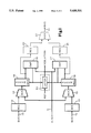
- FIG. 1 is a block diagram view of a zero dead time acquisition system according to the present invention.
- FIG. 2 is a diagrammatic representation view of a post-trigger acquisition memory.
- FIG. 3 is a timing diagram view for zero dead time acquisition of post-trigger data samples according to the present invention.
- FIG. 4 is a diagrammatic representation view of a pre-trigger acquisition memory according to the present invention.
- FIG. 5 is a block timing diagram view for zero dead time acquisition when pre-trigger data samples are acquired according to the present invention.
- a first input buffer 12 and a second input buffer 13 are shown coupled to receive data from a data bus 10, which in turn is coupled to an acquisition memory and/or to a waveform specification memory.
- a stream of digitized data samples on line 11, representing an electrical signal is input to a pair of input multiplexers 14, 15 and to a pair of comparators 16, 17.
- the other inputs to the pair of multiplexers 14, 15 are the outputs from the input buffers 12, 13, respectively.
- the outputs from the multiplexers 14, 15 are input to respective accumulators 18, 19 together with the outputs from the comparators 16, 17.
- the outputs from the comparators 16, 17 provide write enable signals to the accumulators 18, 19.
- the outputs from the accumulators 18, 19 are coupled as second inputs to the comparators 16, 17.
- the outputs from the accumulators 18, 19 also are coupled as inputs to respective output buffers 20, 21.
- the outputs of the output buffers 20, 21 are input to an output multiplexer 22, the output of which is coupled to the data bus 10.
- the outputs from the comparators 16, 17 also may be input to respective set inputs of a latch 24.
- the output of the latch 24 provides an error signal when in the save-on-delta mode to indicate that the electrical signal is outside design parameters, as indicated by a waveform specification, or template, stored in the waveform specification memory.
- an acquisition memory 26 for post-trigger acquisition in the envelope mode contains accumulated samples from the digitized data samples that occur after a trigger event.
- the accumulated samples represent MIN/MAX data pairs from prior acquisition cycles from the first sample interval after the trigger event (MIN/MAX0) to the end of the memory (MIN/MAXn).
- the acquisition memory 26 is initialized with all MAX locations having "00" and all MIN locations having "ff". As shown in FIG.
- MIN/MAX0 are loaded from the acquisition memory 26 via the data bus 10 into the respective input buffers 12, 13 and at the first sample clock after the first trigger signal, which is the beginning of a sample interval, the MIN/MAX0 values are transferred via the respective multiplexers 14, 15 to "seed" the respective accumulators 18, 19 with initial reference samples.
- the first accumulation occurs if the values in the accumulators 18, 19 produce an output signal from the comparators 16, 17 due to the corresponding data value in the digitized data samples "exceeding" the accumulator value.
- one of the input buffers 12, 13 is loaded with the next value from the acquisition memory 26, and on the next sample clock the other input buffer 13, 12 is loaded with the following value from the acquisition memory so that the input buffers are loaded with the next min/max data pair (MIN/MAX1).
- the corresponding digitized data samples are compared with the reference samples from the accumulators 18, 19 by the respective comparators 16, 17. If any of the digitized data samples within the sample interval fall outside of the limits determined by the reference samples, the appropriate accumulator 18, 19 is enabled by the corresponding comparator 16, 17 output.
- the reference sample that is "exceeded” then is replaced in the appropriate accumulator 18, 19 via the appropriate input multiplexer 14, 15 by the digitized data sample that caused the out of limits condition.
- the reference samples from the accumulators 18, 19 are transferred to the output buffers 20, 21 and the next MAX/MIN samples from the acquisition memory 26, which were loaded into the input buffers 12, 13 during the previous sample interval, are loaded from the input buffers into the accumulators.
- the MIN and MAX values from the output buffers 20, 21 are transferred to the appropriate locations in the acquisition memory 26 via the data bus 10, replacing the former MIN/MAX values. Then the MIN/MAX values for the following sample interval are loaded into the input buffers 12, 13, as discussed above.
- the post-trigger mode described above is simple because the time relationships between the data samples accumulated and the trigger signal are known. In the pre-trigger mode no relationships between data samples and the trigger signal are known while the data samples are being acquired since the trigger event has not yet occurred. Therefore it is not possible to know which data samples to accumulate in which memory locations before hand.
- the problem is solved by comparing the pre-trigger accumulated data samples with prior pre-trigger accumulated data samples during the acquisition of pre-trigger data samples on the next acquisition cycle. As shown in FIG. 4 the acquisition memory 26' is divided into four sections, a first pre-trigger section 27, a second pre-trigger section 28, a processed/template pre-trigger section 29 and a post-trigger section 30.
- the first two sections 27, 28 of the acquisition memory 26' are circulating memories for acquiring data samples during the pre-trigger sample intervals.
- the sequence of operation in the envelope mode for pre-trigger is described below with respect to FIG. 5.
- the pre-trigger sections 27, 28 alternate, i.e., during one acquisition cycle one pre-trigger section is used and during the next acquisition cycle the other pre-trigger section is used.
- the digitized data samples are applied via the input multiplexers 14, 15 directly to the accumulators 18, 19, i.e., the input buffers 12, 13 are not used.
- the first digitized data sample is loaded into the accumulators 18, 19 initially and then compared with subsequent digitized data samples within the sample interval such that at the end of the sample interval the accumulators reflect the maximum/minimum data samples during that sample interval.
- the min/max data samples are transferred to the output buffers 20, 21 and stored in the next location in the accessed pre-trigger section 27, 28 of the acquisition memory 26'. Once the trigger signal occurs the post-trigger data samples are accumulated in the post-trigger section 30 of the acquisition memory 26', as described above.
- the locations of the pre-trigger data samples in the appropriate pre-trigger section 27, 28 are now definitively known so that, as the other pre-trigger section 28, 27 is being accessed and filled, the data samples from the prior pre-trigger section 27, 28 are being compared with the corresponding data samples as reference samples from the processed pre-trigger section 29, with the data samples from the pre-trigger section replacing the data samples in the processed pre-trigger section if they "exceed" the max/min values represented by the processed data samples.
- the MAX/MIN values for the pre-trigger data samples are finally determined after the acquisition cycle during the pre-trigger cycle of the next acquisition cycle.
- the processed pre-trigger and post-trigger sections 29, 30 form the portion of the acquisition memory 26, that is used to display the analog waveform.
- first pre-trigger section 27 In summary acquisition starts with normal MIN/MAX decimation in the first pre-trigger section 27 in a circular manner. Thus the first pre-trigger section accumulates values for each sample interval. After pre-trigger fill time, i.e., the minimum amount of time required to fill the first pre-trigger section 27 as determined by an operator, a trigger signal occurs and post-trigger accumulation occurs in the post-trigger section 30 as described above. After post-trigger accumulation is completed, hold-off time, if any, is asserted. After hold-off two processes are overlapped. Pre-trigger acquisition of MIN/MAX pairs occurs into the second pre-trigger section 28, and MIN/MAX accumulation occurs between the first pre-trigger section 27 and the processed pre-trigger section 29.
- pre-trigger fill time i.e., the minimum amount of time required to fill the first pre-trigger section 27 as determined by an operator
- post-trigger accumulation After post-trigger accumulation is completed, hold-off time, if any,
- the values loaded into a waveform specification memory are MAX/MIN limit values that define a template. Any digitized data points that fall outside the template represent an error condition, and subsequent acquisition cycles are terminated so that the current acquisition cycle may be captured for subsequent examination. Once transferred from the acquisition memory 26, the acquisition may then continue.
- the save-on-delta mode circuitry is then similar to the envelope mode circuitry except that the input multiplexers 14, 15 may be deleted since only the template via the input buffers 12, 13 is loaded into the accumulators 18, 19 at the beginning of each sample interval.
- the output buffers 20, 21 and output multiplexer 22 are not needed since the template is not changed, and thus there is no need to change the data in the memory 26. Further the outputs of the comparators 16, 17 are applied to the error latch 24 rather than to the accumulators 18, 19. If as a result of a comparison there is an out-of-limit condition, the latch 24 is set by the output of the comparator 16, 17 detecting the condition to provide the error signal. The latch 24 is reset at the beginning of each acquisition.
- the corresponding template values from the memory 26 are loaded via the input buffers 12, 13 into the accumulators 18, 19 for comparison with the digitized samples.
- the latch 24 is set to generate the error signal.
- the acquired pre-trigger data is compared with the pre-trigger template values stored in the processed/template pre-trigger section 29 of the memory 26' while the next acquisition cycle is acquiring pre-trigger data samples.
- the next acquisition cycle is terminated at the occurrence of the trigger signal, prior to post-trigger data acquisition, so that the resulting stored waveform, including both pre-trigger and post-trigger data samples, may be transferred to main memory to save the portion of the analog signal having an error condition.
- the acquisition is reinitialized and the latch 24 is reset to start acquiring the waveform again.
- the present invention provides zero dead time acquisition for a digital storage oscilloscope in a decimation/accumulation mode of operation, using either envelope or save-on-delta modes, by comparing incoming digitized data with values from an acquisition memory that represent either accumulated data for a prior acquisition or a waveform specification, or template.
Landscapes
- Physics & Mathematics (AREA)
- General Physics & Mathematics (AREA)
- Analogue/Digital Conversion (AREA)
- Measurement Of Current Or Voltage (AREA)
Priority Applications (2)
| Application Number | Priority Date | Filing Date | Title |
|---|---|---|---|
| US08/085,368 US5438531A (en) | 1993-07-02 | 1993-07-02 | Zero dead time acquisition for a digital storage oscilloscope |
| JP6174764A JP2733740B2 (ja) | 1993-07-02 | 1994-07-04 | 信号取込み装置及び方法 |
Applications Claiming Priority (1)
| Application Number | Priority Date | Filing Date | Title |
|---|---|---|---|
| US08/085,368 US5438531A (en) | 1993-07-02 | 1993-07-02 | Zero dead time acquisition for a digital storage oscilloscope |
Publications (1)
| Publication Number | Publication Date |
|---|---|
| US5438531A true US5438531A (en) | 1995-08-01 |
Family
ID=22191158
Family Applications (1)
| Application Number | Title | Priority Date | Filing Date |
|---|---|---|---|
| US08/085,368 Expired - Lifetime US5438531A (en) | 1993-07-02 | 1993-07-02 | Zero dead time acquisition for a digital storage oscilloscope |
Country Status (2)
| Country | Link |
|---|---|
| US (1) | US5438531A (ja) |
| JP (1) | JP2733740B2 (ja) |
Cited By (12)
| Publication number | Priority date | Publication date | Assignee | Title |
|---|---|---|---|---|
| US5740064A (en) * | 1996-01-16 | 1998-04-14 | Hewlett-Packard Co. | Sampling technique for waveform measuring instruments |
| US5779638A (en) * | 1995-03-28 | 1998-07-14 | Sonometrics Corporation | Ultrasound-based 3-D tracking system using a digital signal processor |
| US6748335B2 (en) * | 2002-05-06 | 2004-06-08 | Tektronix, Inc. | Acquisition system for a multi-channel relatively long record length digital storage oscilloscope |
| US6760673B2 (en) * | 2002-07-31 | 2004-07-06 | Agilent Technologies, Inc. | Method and apparatus for waveform measurement instrument |
| US20040189636A1 (en) * | 2003-03-27 | 2004-09-30 | Azinger Frederick A. | Automated storage of unique waveforms presented as an oscilloscope image |
| US6807496B2 (en) * | 2002-05-02 | 2004-10-19 | Tektronix, Inc. | Acquisition system for a long record length digital storage oscilloscope |
| US20060074607A1 (en) * | 2004-09-28 | 2006-04-06 | Weller Dennis J | Digital trigger filter for a real time digital oscilloscope |
| US20080177508A1 (en) * | 2006-08-02 | 2008-07-24 | Tektronix, Inc. | Noise reduction filter for trigger circuit |
| US20100023637A1 (en) * | 2008-07-23 | 2010-01-28 | Qualcomm Incorporated | System, method or apparatus for combining multiple streams of media data |
| CN104133729A (zh) * | 2014-07-29 | 2014-11-05 | 中国电子科技集团公司第四十一研究所 | 一种高速无死区测频时随机错误的修正方法 |
| US20170003328A1 (en) * | 2015-06-30 | 2017-01-05 | University Of Electronic Science And Technology Of China | Method for measuring the waveform capture rate of a digital storage oscilloscope based on average dead time measurement |
| US10677817B2 (en) | 2017-11-14 | 2020-06-09 | University Of Electronic Science And Technology Of China | Method for oscilloscope 3D mapping in scan mode |
Families Citing this family (3)
| Publication number | Priority date | Publication date | Assignee | Title |
|---|---|---|---|---|
| US8024141B2 (en) * | 2009-09-04 | 2011-09-20 | Tektronix, Inc. | Test and measurement instrument and method for providing post-acquisition trigger control and presentation |
| US20110060540A1 (en) * | 2009-09-04 | 2011-03-10 | Tektronix, Inc. | Test and Measurement Instrument and Method For Providing Post-Acquisition Trigger Control and Presentation |
| CN114509589B (zh) * | 2020-11-17 | 2025-11-25 | 北京普源精电科技有限公司 | 示波器的触发系统、触发方法、示波器以及存储介质 |
Citations (1)
| Publication number | Priority date | Publication date | Assignee | Title |
|---|---|---|---|---|
| US4326261A (en) * | 1980-06-23 | 1982-04-20 | Peoples John T | Single tone detector |
Family Cites Families (5)
| Publication number | Priority date | Publication date | Assignee | Title |
|---|---|---|---|---|
| DE3744398A1 (de) * | 1987-12-29 | 1989-07-13 | Asea Brown Boveri | Verfahren und vorrichtung zur registrierung von signalkurven |
| JPH01185448A (ja) * | 1988-01-21 | 1989-07-25 | Matsushita Electric Ind Co Ltd | ディジタルオシロスコープ |
| DE3878232T2 (de) * | 1988-07-12 | 1993-05-27 | Le Croy S A | Methode und einrichtung zur kompression digitaler zeitserieller daten fuer die anzeige auf einem digital-oszilloskop. |
| JPH02138877A (ja) * | 1988-11-18 | 1990-05-28 | Yokogawa Electric Corp | 波形記憶装置 |
| JPH0519032A (ja) * | 1991-07-12 | 1993-01-26 | Jeol Ltd | スペクトルデータの圧縮処理装置 |
-
1993
- 1993-07-02 US US08/085,368 patent/US5438531A/en not_active Expired - Lifetime
-
1994
- 1994-07-04 JP JP6174764A patent/JP2733740B2/ja not_active Expired - Fee Related
Patent Citations (1)
| Publication number | Priority date | Publication date | Assignee | Title |
|---|---|---|---|---|
| US4326261A (en) * | 1980-06-23 | 1982-04-20 | Peoples John T | Single tone detector |
Cited By (18)
| Publication number | Priority date | Publication date | Assignee | Title |
|---|---|---|---|---|
| US5779638A (en) * | 1995-03-28 | 1998-07-14 | Sonometrics Corporation | Ultrasound-based 3-D tracking system using a digital signal processor |
| US5740064A (en) * | 1996-01-16 | 1998-04-14 | Hewlett-Packard Co. | Sampling technique for waveform measuring instruments |
| WO1998046140A1 (en) * | 1997-04-17 | 1998-10-22 | Sonometrics Corporation | Ultrasound-based 3-d tracking system using a digital signal processor |
| US6807496B2 (en) * | 2002-05-02 | 2004-10-19 | Tektronix, Inc. | Acquisition system for a long record length digital storage oscilloscope |
| US6748335B2 (en) * | 2002-05-06 | 2004-06-08 | Tektronix, Inc. | Acquisition system for a multi-channel relatively long record length digital storage oscilloscope |
| US6760673B2 (en) * | 2002-07-31 | 2004-07-06 | Agilent Technologies, Inc. | Method and apparatus for waveform measurement instrument |
| US20040189636A1 (en) * | 2003-03-27 | 2004-09-30 | Azinger Frederick A. | Automated storage of unique waveforms presented as an oscilloscope image |
| US7072804B2 (en) * | 2004-09-28 | 2006-07-04 | Agilent Technologies, Inc. | Digital trigger filter for a real time digital oscilloscope |
| US20060074607A1 (en) * | 2004-09-28 | 2006-04-06 | Weller Dennis J | Digital trigger filter for a real time digital oscilloscope |
| US20080177508A1 (en) * | 2006-08-02 | 2008-07-24 | Tektronix, Inc. | Noise reduction filter for trigger circuit |
| US7610178B2 (en) | 2006-08-02 | 2009-10-27 | Tektronix, Inc. | Noise reduction filter for trigger circuit |
| US20100023637A1 (en) * | 2008-07-23 | 2010-01-28 | Qualcomm Incorporated | System, method or apparatus for combining multiple streams of media data |
| US8762561B2 (en) | 2008-07-23 | 2014-06-24 | Qualcomm Incorporated | System, method or apparatus for combining multiple streams of media data |
| CN104133729A (zh) * | 2014-07-29 | 2014-11-05 | 中国电子科技集团公司第四十一研究所 | 一种高速无死区测频时随机错误的修正方法 |
| CN104133729B (zh) * | 2014-07-29 | 2017-06-20 | 中国电子科技集团公司第四十一研究所 | 一种高速无死区测频时随机错误的修正方法 |
| US20170003328A1 (en) * | 2015-06-30 | 2017-01-05 | University Of Electronic Science And Technology Of China | Method for measuring the waveform capture rate of a digital storage oscilloscope based on average dead time measurement |
| US10119997B2 (en) * | 2015-06-30 | 2018-11-06 | University Of Electronic Science And Technology Of China | Method for measuring the waveform capture rate of a digital storage oscilloscope based on average dead time measurement |
| US10677817B2 (en) | 2017-11-14 | 2020-06-09 | University Of Electronic Science And Technology Of China | Method for oscilloscope 3D mapping in scan mode |
Also Published As
| Publication number | Publication date |
|---|---|
| JP2733740B2 (ja) | 1998-03-30 |
| JPH0735781A (ja) | 1995-02-07 |
Similar Documents
| Publication | Publication Date | Title |
|---|---|---|
| US5438531A (en) | Zero dead time acquisition for a digital storage oscilloscope | |
| US4975636A (en) | Method and apparatus for selecting and displaying a high resolution window from a main display | |
| US4271486A (en) | Waveform storage system | |
| JP3300850B2 (ja) | デジタル・オシロスコープ | |
| US4495586A (en) | Waveform acquisition apparatus and method | |
| US8046183B2 (en) | Pre-trigger and post-trigger acquisition for no dead time acquisition system | |
| US4183087A (en) | Peak deviation sampling | |
| EP0120569B1 (en) | Digital signal sampling system with two unrelated sampling timebases | |
| US4555765A (en) | Multi-mode oscilloscope trigger with compensating trigger delay | |
| US5999163A (en) | Digital oscilloscope with high live time recording of signal anomalies and method | |
| US6847905B2 (en) | Architecture providing increased information display for long acquisitions or constrained memory bandwidth | |
| US5180971A (en) | Method and apparatus for increasing throughput in random repetitive digitizing systems | |
| JPS5875068A (ja) | 波形蓄積表示装置 | |
| US5115404A (en) | Digital storage oscilloscope with indication of aliased display | |
| US5315627A (en) | Pseudo-random repetitive sampling of a signal | |
| US5898420A (en) | Instrument with maximum display update rate and maximized display bandwidth given the display update rate | |
| US5212485A (en) | Analog oscilloscope digitizer | |
| US5153501A (en) | Waveform measuring device | |
| EP0004152A1 (en) | Digitizing a recurring analog signal | |
| US4729011A (en) | Method and apparatus for digitizing television signals | |
| EP1783505B1 (en) | Compressed logic sample storage | |
| US5268851A (en) | Detection of metastability in triggers | |
| JPS63277975A (ja) | トリガー事象捕促装置 | |
| JPH10293140A (ja) | ランダム・サンプリングのホールドオフ方法と回路 | |
| JPH10336030A (ja) | ランダム・サンプリングのトリガ・ホールドオフ方法と回路 |
Legal Events
| Date | Code | Title | Description |
|---|---|---|---|
| STPP | Information on status: patent application and granting procedure in general |
Free format text: APPLICATION UNDERGOING PREEXAM PROCESSING |
|
| AS | Assignment |
Owner name: TEKTRONIX, INC., OREGON Free format text: ASSIGNMENT OF ASSIGNORS INTEREST;ASSIGNOR:SHANK, GORDON W.;REEL/FRAME:007453/0221 Effective date: 19930628 |
|
| FEPP | Fee payment procedure |
Free format text: PAYOR NUMBER ASSIGNED (ORIGINAL EVENT CODE: ASPN); ENTITY STATUS OF PATENT OWNER: LARGE ENTITY |
|
| FPAY | Fee payment |
Year of fee payment: 4 |
|
| AS | Assignment |
Owner name: CONTINENTAL ACQUISITION CORP., MISSOURI Free format text: ASSIGNMENT OF ASSIGNORS INTEREST;ASSIGNOR:CONTICO INTERNATIONAL, INC.;REEL/FRAME:010288/0051 Effective date: 19990716 |
|
| FPAY | Fee payment |
Year of fee payment: 8 |
|
| FPAY | Fee payment |
Year of fee payment: 12 |