US5527740A - Manufacturing dual sided wire bonded integrated circuit chip packages using offset wire bonds and support block cavities - Google Patents
Manufacturing dual sided wire bonded integrated circuit chip packages using offset wire bonds and support block cavities Download PDFInfo
- Publication number
- US5527740A US5527740A US08/267,878 US26787894A US5527740A US 5527740 A US5527740 A US 5527740A US 26787894 A US26787894 A US 26787894A US 5527740 A US5527740 A US 5527740A
- Authority
- US
- United States
- Prior art keywords
- leadframe
- integrated circuit
- support block
- die
- circuit die
- Prior art date
- Legal status (The legal status is an assumption and is not a legal conclusion. Google has not performed a legal analysis and makes no representation as to the accuracy of the status listed.)
- Expired - Lifetime
Links
Images




Classifications
-
- H—ELECTRICITY
- H10—SEMICONDUCTOR DEVICES; ELECTRIC SOLID-STATE DEVICES NOT OTHERWISE PROVIDED FOR
- H10W—GENERIC PACKAGES, INTERCONNECTIONS, CONNECTORS OR OTHER CONSTRUCTIONAL DETAILS OF DEVICES COVERED BY CLASS H10
- H10W90/00—Package configurations
- H10W90/811—Multiple chips on leadframes
-
- H—ELECTRICITY
- H10—SEMICONDUCTOR DEVICES; ELECTRIC SOLID-STATE DEVICES NOT OTHERWISE PROVIDED FOR
- H10W—GENERIC PACKAGES, INTERCONNECTIONS, CONNECTORS OR OTHER CONSTRUCTIONAL DETAILS OF DEVICES COVERED BY CLASS H10
- H10W72/00—Interconnections or connectors in packages
- H10W72/01—Manufacture or treatment
- H10W72/0198—Manufacture or treatment batch processes
-
- H—ELECTRICITY
- H10—SEMICONDUCTOR DEVICES; ELECTRIC SOLID-STATE DEVICES NOT OTHERWISE PROVIDED FOR
- H10W—GENERIC PACKAGES, INTERCONNECTIONS, CONNECTORS OR OTHER CONSTRUCTIONAL DETAILS OF DEVICES COVERED BY CLASS H10
- H10W72/00—Interconnections or connectors in packages
- H10W72/071—Connecting or disconnecting
- H10W72/0711—Apparatus therefor
- H10W72/07178—Means for aligning
-
- H—ELECTRICITY
- H10—SEMICONDUCTOR DEVICES; ELECTRIC SOLID-STATE DEVICES NOT OTHERWISE PROVIDED FOR
- H10W—GENERIC PACKAGES, INTERCONNECTIONS, CONNECTORS OR OTHER CONSTRUCTIONAL DETAILS OF DEVICES COVERED BY CLASS H10
- H10W72/00—Interconnections or connectors in packages
- H10W72/071—Connecting or disconnecting
- H10W72/073—Connecting or disconnecting of die-attach connectors
-
- H—ELECTRICITY
- H10—SEMICONDUCTOR DEVICES; ELECTRIC SOLID-STATE DEVICES NOT OTHERWISE PROVIDED FOR
- H10W—GENERIC PACKAGES, INTERCONNECTIONS, CONNECTORS OR OTHER CONSTRUCTIONAL DETAILS OF DEVICES COVERED BY CLASS H10
- H10W72/00—Interconnections or connectors in packages
- H10W72/071—Connecting or disconnecting
- H10W72/075—Connecting or disconnecting of bond wires
-
- H—ELECTRICITY
- H10—SEMICONDUCTOR DEVICES; ELECTRIC SOLID-STATE DEVICES NOT OTHERWISE PROVIDED FOR
- H10W—GENERIC PACKAGES, INTERCONNECTIONS, CONNECTORS OR OTHER CONSTRUCTIONAL DETAILS OF DEVICES COVERED BY CLASS H10
- H10W72/00—Interconnections or connectors in packages
- H10W72/50—Bond wires
- H10W72/531—Shapes of wire connectors
- H10W72/536—Shapes of wire connectors the connected ends being ball-shaped
-
- H—ELECTRICITY
- H10—SEMICONDUCTOR DEVICES; ELECTRIC SOLID-STATE DEVICES NOT OTHERWISE PROVIDED FOR
- H10W—GENERIC PACKAGES, INTERCONNECTIONS, CONNECTORS OR OTHER CONSTRUCTIONAL DETAILS OF DEVICES COVERED BY CLASS H10
- H10W72/00—Interconnections or connectors in packages
- H10W72/50—Bond wires
- H10W72/531—Shapes of wire connectors
- H10W72/5363—Shapes of wire connectors the connected ends being wedge-shaped
-
- H—ELECTRICITY
- H10—SEMICONDUCTOR DEVICES; ELECTRIC SOLID-STATE DEVICES NOT OTHERWISE PROVIDED FOR
- H10W—GENERIC PACKAGES, INTERCONNECTIONS, CONNECTORS OR OTHER CONSTRUCTIONAL DETAILS OF DEVICES COVERED BY CLASS H10
- H10W72/00—Interconnections or connectors in packages
- H10W72/50—Bond wires
- H10W72/541—Dispositions of bond wires
- H10W72/5449—Dispositions of bond wires not being orthogonal to a side surface of the chip, e.g. fan-out arrangements
-
- H—ELECTRICITY
- H10—SEMICONDUCTOR DEVICES; ELECTRIC SOLID-STATE DEVICES NOT OTHERWISE PROVIDED FOR
- H10W—GENERIC PACKAGES, INTERCONNECTIONS, CONNECTORS OR OTHER CONSTRUCTIONAL DETAILS OF DEVICES COVERED BY CLASS H10
- H10W72/00—Interconnections or connectors in packages
- H10W72/50—Bond wires
- H10W72/551—Materials of bond wires
- H10W72/552—Materials of bond wires comprising metals or metalloids, e.g. silver
- H10W72/5522—Materials of bond wires comprising metals or metalloids, e.g. silver comprising gold [Au]
-
- H—ELECTRICITY
- H10—SEMICONDUCTOR DEVICES; ELECTRIC SOLID-STATE DEVICES NOT OTHERWISE PROVIDED FOR
- H10W—GENERIC PACKAGES, INTERCONNECTIONS, CONNECTORS OR OTHER CONSTRUCTIONAL DETAILS OF DEVICES COVERED BY CLASS H10
- H10W72/00—Interconnections or connectors in packages
- H10W72/851—Dispositions of multiple connectors or interconnections
- H10W72/874—On different surfaces
- H10W72/884—Die-attach connectors and bond wires
-
- H—ELECTRICITY
- H10—SEMICONDUCTOR DEVICES; ELECTRIC SOLID-STATE DEVICES NOT OTHERWISE PROVIDED FOR
- H10W—GENERIC PACKAGES, INTERCONNECTIONS, CONNECTORS OR OTHER CONSTRUCTIONAL DETAILS OF DEVICES COVERED BY CLASS H10
- H10W74/00—Encapsulations, e.g. protective coatings
-
- H—ELECTRICITY
- H10—SEMICONDUCTOR DEVICES; ELECTRIC SOLID-STATE DEVICES NOT OTHERWISE PROVIDED FOR
- H10W—GENERIC PACKAGES, INTERCONNECTIONS, CONNECTORS OR OTHER CONSTRUCTIONAL DETAILS OF DEVICES COVERED BY CLASS H10
- H10W90/00—Package configurations
- H10W90/701—Package configurations characterised by the relative positions of pads or connectors relative to package parts
- H10W90/731—Package configurations characterised by the relative positions of pads or connectors relative to package parts of die-attach connectors
- H10W90/736—Package configurations characterised by the relative positions of pads or connectors relative to package parts of die-attach connectors between a chip and a stacked lead frame, conducting package substrate or heat sink
-
- H—ELECTRICITY
- H10—SEMICONDUCTOR DEVICES; ELECTRIC SOLID-STATE DEVICES NOT OTHERWISE PROVIDED FOR
- H10W—GENERIC PACKAGES, INTERCONNECTIONS, CONNECTORS OR OTHER CONSTRUCTIONAL DETAILS OF DEVICES COVERED BY CLASS H10
- H10W90/00—Package configurations
- H10W90/701—Package configurations characterised by the relative positions of pads or connectors relative to package parts
- H10W90/751—Package configurations characterised by the relative positions of pads or connectors relative to package parts of bond wires
- H10W90/756—Package configurations characterised by the relative positions of pads or connectors relative to package parts of bond wires between a chip and a stacked lead frame, conducting package substrate or heat sink
-
- H—ELECTRICITY
- H10—SEMICONDUCTOR DEVICES; ELECTRIC SOLID-STATE DEVICES NOT OTHERWISE PROVIDED FOR
- H10W—GENERIC PACKAGES, INTERCONNECTIONS, CONNECTORS OR OTHER CONSTRUCTIONAL DETAILS OF DEVICES COVERED BY CLASS H10
- H10W99/00—Subject matter not provided for in other groups of this subclass
-
- Y—GENERAL TAGGING OF NEW TECHNOLOGICAL DEVELOPMENTS; GENERAL TAGGING OF CROSS-SECTIONAL TECHNOLOGIES SPANNING OVER SEVERAL SECTIONS OF THE IPC; TECHNICAL SUBJECTS COVERED BY FORMER USPC CROSS-REFERENCE ART COLLECTIONS [XRACs] AND DIGESTS
- Y10—TECHNICAL SUBJECTS COVERED BY FORMER USPC
- Y10T—TECHNICAL SUBJECTS COVERED BY FORMER US CLASSIFICATION
- Y10T29/00—Metal working
- Y10T29/49—Method of mechanical manufacture
- Y10T29/49002—Electrical device making
- Y10T29/49117—Conductor or circuit manufacturing
- Y10T29/49121—Beam lead frame or beam lead device
Definitions
- the present invention pertains to the field of integrated circuit die packaging. More particularly, this invention relates to constructing a dual sided integrated circuit chip package that employs wire bond process technology with offset wire bonds and support blocks with cavities for stitch bonding support.
- Plastic chip packages are commonly employed for holding integrated circuit dies.
- a typical prior plastic package is constructed on a section of a metal leadframe.
- Each leadframe section provides a die pad for mounting an integrated circuit die.
- Each leadframe section also provides a set of lead fingers for electrical connection between the corresponding integrated circuit die and external circuitry.
- Such a plastic package provides protection for the integrated circuit die and provides electrical connection to the integrated circuit die via the lead fingers extending from the package.
- Such prior plastic chip packages typically contain one integrated circuit die per package.
- the integrated circuit die is typically mounted on one side of a die pad.
- the integrated circuit is usually mounted on either the top or the bottom side of the die pad.
- the integrated circuit die, attached to a die pad is wire bonded to corresponding lead fingers.
- the die pad, the integrated circuit die, and the wire bonding are typically encapsulated with molding compound through plastic injection molding or with glob top.
- an integrated circuit chip package can be increased by enclosing two or more integrated circuit dies in one chip package.
- an integrated circuit die package containing two memory chips can double the density of a memory system without increasing the printed circuit board area containing the memory chips.
- Another example is an integrated circuit die package containing a microcontroller or processor on one side and a memory chip on the other side.
- TAB tape automated bonding
- One object of the present invention is to provide a dual sided integrated circuit chip package containing two or more integrated circuit chips having similar or differing dimensions and performing similar or differing functions.
- Another object of the present invention is to provide a method for manufacturing a dual sided integrated circuit chip package that includes a single plastic molding step for each package.
- Another object of the present invention is to provide a dual sided integrated circuit chip package that employs offset stitch wire bonds on opposite sides of a leadframe.
- a further object of the present invention is to provide a method for manufacturing a dual sided integrated circuit chip package that employs support blocks having cavities that accept integrated circuit dies during die attach and wire bond process steps.
- Another object of the present invention is to provide a method for manufacturing a dual sided integrated circuit chip package that employs support and or clamping blocks having cavities that provide clearance for previously formed stitch bonds while providing support for newly formed stitch bonds.
- Another object of the present invention is to provide a method for manufacturing a dual sided integrated circuit chip package that reduces vibration during wire bonding steps to prevent and or minimize defects such as bond cratering of bond pads or die cracking.
- Another object is to enhance efficiency and utilization of production equipment by outputting more functionality per equipment and enhancing reliability of the resultant package.
- a leadflame is formed having at least one die pad and a set of lead fingers corresponding to the die pad.
- An integrated circuit die is attached onto a first side of the die pad and the first side die attach is cured.
- An integrated circuit die is then attached onto the second side of the die pad while the leadframe is supported with a die surface contactless support block having a cavity that accepts the side two integrated circuit die and the second side die attach is cured.
- the side two integrated circuit die is wire bonded to the corresponding lead fingers while the leadframe is supported with a support and clamping block having a cavity that accepts the side one integrated circuit die and that supports the end of each lead finger.
- the side one integrated circuit die is wire bonded to the corresponding lead fingers while the die pad is supported with a die surface contactless support block having a cavity that accepts the side two integrated circuit die and corresponding wire bonds while each lead finger is supported and providing clearance for a stitch bond of each wire bond on side two of the leadframe.
- the sequence of wire bonding can be reversed, e.g., wire bond side two first and wire bond side one later.
- a one step plastic mold is formed around the assembly comprising the first and second integrated circuit dies, the die pads and the wire bonds.
- the leadframe is formed and a side one integrated circuit die is disposed onto the first side of the die pad.
- the side one integrated circuit die is then wire bonded to the first side the corresponding lead fingers while the leadframe is supported with either a flat support block or a support block having a cavity.
- a side two integrated circuit die is disposed onto the second side of the die pad while the leadframe is supported with the support and clamping block having the cavity that accepts the side one integrated circuit die and corresponding wire bonds.
- the side two integrated circuit die is then wire bonded to the second side of the corresponding lead fingers while the leadframe is supported with the support block having the cavity, and then a one step plastic mold is formed around the assembly comprising the first and second integrated circuit dies, the die pads and the wire bonds. The sequence of wire bonding is reversible.
- FIG. 1 is a top view showing one side of a leadframe which forms a set of die pads that provide mounting platforms for integrated circuit dies for one embodiment;
- FIG. 2 is a top view of the leadframe which shows the die pads and corresponding lead fingers which enable electrical coupling to the integrated circuit dies mounted to the die pad;
- FIG. 3 is a flow chart that illustrates a series of process steps applied to the leadframe to form a dual sided wire bonded plastic chip package onto each of the die pads for one embodiment
- FIG. 4 is a cross sectional view of the leadframe along a section 4--4 which shows an integrated circuit die attached to side one of the die pad using an adhesive layer;
- FIG. 5a is a cross sectional view along section 4--4 of the leadframe which shows a cavity of the support block that provides clearance for the side one integrated circuit die during side two die attach;
- FIG. 5b is a cross sectional view along section 4--4 of the leadframe which shows a cavity of the support block that provides clearance for the side one integrated circuit die and which shows clamping blocks during side two wire bonding;
- FIG. 6 is a cross sectional view along section 6--6 of the leadframe that shows wire bonding of the side two integrated circuit die to the lead fingers;
- FIG. 7 is a cross sectional view along section 6--6 of the leadframe that shows the wire bonding of the side one integrated circuit die to the lead fingers of the leadframe;
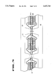
- FIG. 8 is a bottom view of a dual sided integrated circuit assembly comprising the side one and two integrated circuit dies and corresponding wire bonds formed on the die pad and shows the location of the support block cavity wherein only one end of each integrated circuit die is shown wire bonded;
- FIG. 9 is a cross sectional view of the integrated circuit die assemblies on the leadframe positioned in an injection mold press during a single step injection mold;
- FIG. 10 is a cross sectional view of a dual sided plastic chip package which comprises the side one and two integrated circuit dies mounted on opposite sides of a die pad and enclosed by a plastic mold;
- FIG. 11 illustrates a series of process steps applied to the leadframe to form a dual sided plastic chip package on each of the die pads for another embodiment
- FIG. 12 is a cross sectional view of the leadframe along section 6--6 shows the leadframe mounted on a flat support block.
- FIG. 1 is a top view showing one side of a leadframe 20.
- One side of the leadframe 20 is hereinafter referred to as side 1, and the opposite side of the leadframe 20 is referred to as side 2.
- the leadframe 20 forms a set of die pads 22-29.
- the die pads 22-29 provide mounting platforms for integrated circuit dies.
- the leadframe 20 also forms a set of lead fingers corresponding to each of the die pads 22-29.
- the die pads 22-29 and the corresponding lead fingers are etched into the leadframe 20.
- the die pads 22-29 and corresponding lead fingers may be stamped into the leadframe 20.
- the leadframe 20 is preferably constructed from either steel or copper.
- the steel or copper materials are selected for interactive properties with silicon and plastic.
- the leadframe 20 is typically 5 mils thick.
- a set of alignment holes such as alignment holes 21, are employed to precisely position the leadframe 20 during the chip package manufacturing process.
- FIG. 2 is a top view of the leadframe 20, and shows the die pads 24 and 25 and corresponding lead fingers.
- a set of lead fingers 28 and a set of lead fingers 30 correspond to the die pad 24.
- the lead fingers 28 and 30 enable electrical coupling to the integrated circuit dies mounted to the die pad 24.
- a set of lead fingers 40 and a set of lead fingers 42 enable electrical coupling to the integrated circuit dies mounted to the die pad 25.
- a silver plating is deposited on both sides of the die pads 22-29.
- a spot silver plating is also deposited on both sides of the tips of the lead fingers corresponding to the die pads 22-29.
- a spot silver plating is deposited along area 32 of the lead fingers 28, and along area 34 of the lead fingers 30.
- a spot silver plating is deposited along area 33 of the lead fingers 40, and along area 35 of the lead fingers 42.
- the silver plating may be applied to side 1 of the leadframe 20 and then to side 2. Alternatively, the silver plating may be applied to both side 1 and side 2 of the leadframe 20 concurrently.
- the silver plating applied to the die pads 22-29 improves the thermal and electrical conduction between the integrated circuit dies and the die pads 22-29.
- the silver plating to the tips of the lead fingers enables wire bonding of gold signal leads to the leadframe 20.
- the plating step on the die pads 22-29 may be skipped to enhance adhesion between the leadframe 20 and a molding compound.
- the leadframe plating step is simplified by applying a silver plating to the die pads 22-29 as well as the lead fingers. If the die pads 22-29 are not plated along with the lead fingers, a separate masking for the die pads 22-29 is required.
- a gold plating or a palladium plating may be deposited to the die pads 22-29 and the tips of the corresponding lead fingers.
- each die pad 22-29 is extended and a set of guide pin holes are formed into each of the die pads 22-29 of the leadframe 20.
- the guide pin holes on each die pad 22-29 provide structural support for the die pads 22-29 during die attach and wire bonding steps to the leadframe 20.
- a set of guide pin holes 300-305 are formed in the die pad 25.
- the guide pin holes 300-305 receive corresponding guide pins of support blocks to provide structural support during die attach and wire bonding steps during formation of a dual sided integrated circuit die package onto the die pad 25.
- the guide pin holes 300-305 reduce vibration of the die pad 25 during wire bonding and prevent bond cratering during the manufacture of chip packages that contain large integrated circuit dies.
- the guide pin holes 300-305 and guide pins may not be necessary for packaging some integrated circuit dies.
- FIG. 3 is a flow chart that illustrates a series of process steps 200-214 applied to the leadframe 20 for one embodiment.
- the process steps 200-214 are applied to the leadframe 20 to form a dual sided wire bonded plastic chip package onto each of the die pads 22-29.
- an integrated circuit die is attached to each die pad 22-29 on side 1 of the leadframe 20.
- die attach refers to an adhesive eutectic 2100 tape type of process followed by the appropriate cure when necessary.
- FIG. 4 is a cross sectional view of the leadframe 20 along section 4--4 of the die pad 25 during process step 200.
- An integrated circuit die 50 is shown attached to side 1 of the die pad 25 using an adhesive layer 52.
- the die pad 25 is supported by a support block 118.
- the support block 118 includes a set of guide pins (not shown) that are received by the guide pin holes 300-305 during the die attach of process step 200.
- the dimension of the die pad 25 measured from an edge 86 to an edge 87 of the die pad 25 is extended over the normal accommodation of the integrated circuit die 50.
- the extended die pad 25 accommodates the placement of the guide pin holes 300-305.
- the distance between an edge 84 of the integrated circuit die 50 and the edge 86 of the die pad 25 and the distance between an edge 85 of the integrated circuit die 50 and the edge 87 of the die pad 25 may extend between 10 and 30 mils.
- the amount of extension of the die pad 25 past the edges 84 and 85 of the integrated circuit die 50 depends on the overall dimensions of the final plastic chip package that contains the die pad 25.
- the amount of extension of the die pad 25 between the edges 86 and 87 is limited to enable the flow of plastic mold between sides 1 and 2 of the leadframe 20 during the plastic mold at process step 210.
- a die attach machine is employed to attach integrated circuit dies to the die pads 22-29.
- the die attach machine dispenses a die attach paste to form the adhesive layer 52 and then places the integrated circuit die 50 onto the die pad 25 and aligns the integrated circuit die 50 to the leadframe 20.
- the die attach machine takes the integrated circuit die 50 from a silicon wafer prior to placement on the die pad 25.
- the adhesive layer 52 is an epoxy paste that is cured at a high temperature of 180° C. to provide rigid support to the integrated circuit die 50.
- FIG. 5a provides a cross sectional view along section 4--4 of the leadframe 20 at process step 202.
- a cavity 120 of the support block 118 provides clearance for the integrated circuit die 50 and the leadframe 20 is held in place by a vacuum on one side of the leadframe 20 tail.
- An integrated circuit die 90 is shown deposited on side two of the die pad 25 with an adhesive layer 92.
- the integrated circuit dies attached to side 1 of the leadframe 20 are wire bonded to the corresponding lead fingers of the leadframe 20.
- the lead fingers 40 include a lead finger 44 which corresponds to the die pad 25.
- the lead fingers 42 include a lead finger 46 that corresponds to the die pad 25.
- FIG. 5b provides a cross sectional view along section 4--4 of the leadframe 20 at process step 204.
- a pair of clamping blocks 110 and 112 are employed to clamp the die pad 25.
- the clamping block 110 includes a set of holes that receive guide pins (not shown) of the support block 118. The clamping force provided by the clamping blocks 110 and 112 provide increased rigidity and reduce the vibration of the die pad 25 during wire bonding on the integrated circuit die 90.
- the guide pins (not shown) of the support block 118 in conjunction with the clamping blocks 110 and 112 are employed to stretch the die pad 25 between the guide pins.
- the die pad 25 is stretched to further reduce vibration and prevent bond cratering of the signal pads formed on the integrated circuit die 50 during wire bonding on the integrated circuit die 90.
- the adhesive layer 52 in combination with the integrated circuit die 50 provides further rigidity during wire bond steps on the integrated circuit die 90.
- FIG. 6 is a cross sectional view along section 6--6 of the leadframe 20 that shows the wire bonding of the integrated circuit die 50 to the lead fingers 44 and 46 of the leadframe 20.
- a wire bond 56 is coupled between a signal pad 54 on the integrated circuit die 50 and the lead finger 44.
- the wire bond 56 couples to the lead finger 44 through the silver plated area 33 of the lead finger 44.
- a wire bond 58 is coupled between a signal pad 55 and the lead finger 46 through the silver plated area 35.
- the lead fingers 40 including the lead finger 44 are supported by the support block 118.
- the lead fingers 42 including the lead finger 46 are supported by the support block 118.
- the support block 118 also provides heat for the wire bonding process. Higher temperatures during the wire bonding process may require less force and energy which minimizes vibrations during the wire bonding process steps.
- the clamping blocks 110 and 112 increase rigidity and reduce vibration during wire bonding of side one.
- the width of the cavity 120 of the support block 118 between a surface 130 and a surface 132 of the support block 118 is selected to provide wire bond support near the ends of the lead fingers 44 and 46.
- the position of the surface 130 provides support near an end 80 of the lead finger 44, and the position of the surface 132 provides support near an end 82 of the lead finger 46.
- the width of the cavity 120 between the surfaces 130 and 132 provides support that enables the formation of stitch bonds to the lead fingers 44 and 46 near the ends 80 and 82 respectively.
- the integrated circuit dies on side 2 of the leadframe 20 are wire bonded to the corresponding lead fingers of the leadframe 20.
- FIG. 7 illustrates the wire bonding of the integrated circuit die 90 to the lead fingers 44 and 46.
- a wire bond 94 is coupled between a signal pad 93 on the integrated circuit die 90 and the lead finger 44 through a silver plated area 75 on the lead finger 44.
- a wire bond 96 is coupled between a signal pad 95 on the integrated circuit die 90 and the lead finger 46 through a silver plated area 76.
- the lead fingers 44 and 46 are supported by a support block 122.
- the clamping blocks 110 and 112 increase rigidity and reduce vibration during wire bonding of side two.
- the support block 122 forms a cavity 320 that provides clearance for the integrated circuit die 50 and lead fingers 56 and 58 and corresponding stitch bonds on the lead fingers.
- the width of the cavity 320 between a surface 100 and a surface 102 of the support block 122 provides clearance for the stitch bonds to the silver plated areas 33 and 35.
- the positions of the surfaces 100 and 102 provide support for the stitch bonds of the wire bonds 94 and 96 to the silver plated areas 75 and 76.
- the stitch bonds of the wire bonds 94 and 96 are formed away from the ends 80 and 82 of the lead fingers 44 and 46 in comparison to the stitch bonds of the wire bonds 56 and 58.
- the dimensions of the cavity 320 between the surfaces 100 and 102 are selected to provide support beneath the stitch bonds of the wire bonds 94 and 96 as well as clearance for the stitch bonds of the wire bonds 56 and 58.
- the support dimensions provided by the cavity 320 are provided by adjusting the positions of the surface 130 and the surface 132 of the support block 118.
- the support block 118 includes adjustable portions that support the lead fingers of the leadframe 20 and that provide adjustable dimensions for the cavity 120.
- FIG. 8 is a top view of a dual sided integrated circuit assembly comprising the integrated circuit dies 50 and 90 and corresponding wire bonds formed on the die pad 25 during process step 206.
- the guide pin holes 300-305 and the lead fingers 40 and 42 are shown, along with an outline 106 that indicates the vertical surfaces of the cavity 320 including the surfaces 100 and 102 formed by the support block 122.
- Also shown are the wire bonds between the lead fingers 40 and the integrated circuit die 50 including the wire bond 56, and the wire bonds between the lead fingers 42 and the integrated circuit die 90 including the write bond 96.
- FIG. 9 is a cross sectional view of the integrated circuit die assemblies on the leadframe 20 positioned in an injection mold press during process step 210.
- the injection mold press includes a top mold 100 and a bottom mold 102.
- the top and bottom molds 100 and 102 provide a mold cavity for each of the integrated circuit die assemblies on the leadframe 20.
- the top and bottom molds 100 and 102 provide a mold cavity 60 for the integrated circuit die assembly comprising the integrated circuit dies 50 and 90 formed onto the die pad 25.
- a plastic mold injector (not shown) injects plastic into each mold cavity to form a plastic mold around each of the integrated circuit die assemblies on the leadframe 20.
- the holes of the die pads 22-29 including the guide pin holes 300-305 improve the flow of plastic mold around the integrated circuit die assembly on the die pad 25.
- the plastic injection molding step is followed by the necessary curing of the molding compound.
- FIG. 10 is a cross sectional view of a dual sided plastic chip package 130.
- the dual sided plastic chip package 130 comprises the integrated circuit dies 50 and 90 mounted on opposite sides of the die pad 25 and enclosed by a plastic mold 66.
- FIG. 11 illustrates a series of process steps 230-242 applied to the leadframe 20 to form a dual sided plastic chip package on each of the die pads 22-29 for another embodiment.
- an integrated circuit die is attached to side 1 of each of the die pads 22-29.
- the integrated circuit dies attached to side 1 of the leadframe 20 are wire bonded to the corresponding lead fingers of the leadframe 20.
- the leadframe 20 may be supported during process steps 230 and 232 with a support block having clearance cavities as discussed above for process steps 200 through 204.
- FIG. 12 is a cross sectional view of the leadframe 20 along section A of the die pad 25 which shows the leadframe 20 mounted on a flat support block 350 at process steps 230 and 232.
- An integrated circuit die 50 is shown attached to side 1 of the die pad 25 with the adhesive layer 52.
- the wire bond 56 is coupled between the signal pad 54 on the integrated circuit die 50 and the lead finger 44 through the silver plated area 33 of the lead finger 44.
- the wire bond 58 is coupled between the signal pad 55 and the lead finger 46 through the silver plated area 35.
- the flat support block 350 enables the formation of stitch bonds to the lead fingers 44 and 46 near the ends 80 and 82.
- an integrated circuit die is attached to each die 22-29 on side 2 of the leadframe 20.
- the leadframe 20 is mounted on the support block 118 with the cavity 120 providing clearance for the integrated circuit die 50 as described above for process step 202.
- the integrated circuit dies on side 2 of the leadframe 20 are wire bonded to the corresponding lead fingers of the leadframe 20.
- the lead fingers 44 and 46 are supported by the support block 122 which provides the cavity 320 to accommodate the integrated circuit die 50 and lead fingers 56 and 58 and corresponding stitch bonds as described above for process step 206.
- a plastic mold is formed with an injection mold press to encase the integrated circuit dies 50 and 90 into a single plastic molded package as described above for process step 210.
- the lead fingers of the leadframe 20 are electro plated with the lead-tin compound.
- the lead fingers of each of the integrated circuit die assemblies on the leadframe 20 are formed into a final shape.
Landscapes
- Lead Frames For Integrated Circuits (AREA)
- Wire Bonding (AREA)
- Structures Or Materials For Encapsulating Or Coating Semiconductor Devices Or Solid State Devices (AREA)
- Encapsulation Of And Coatings For Semiconductor Or Solid State Devices (AREA)
Priority Applications (9)
| Application Number | Priority Date | Filing Date | Title |
|---|---|---|---|
| US08/267,878 US5527740A (en) | 1994-06-28 | 1994-06-28 | Manufacturing dual sided wire bonded integrated circuit chip packages using offset wire bonds and support block cavities |
| US08/404,534 US5545922A (en) | 1994-06-28 | 1995-03-15 | Dual sided integrated circuit chip package with offset wire bonds and support block cavities |
| MX9606556A MX9606556A (es) | 1994-06-28 | 1995-06-21 | Fabricacion de paquetes de circuitos integrados unidos con alambre por lados duales, utilizando uniones de alambres desplazadas y cavidades de bloque de soporte. |
| EP95924032A EP0774162B1 (de) | 1994-06-28 | 1995-06-21 | Herstellung zweiseitig drahtverbundener intergrierter schaltungschippackungen unter verwendung von offset-drahtverbindungen und trägerplatten mit hohlräumen |
| CN95193835A CN1104045C (zh) | 1994-06-28 | 1995-06-21 | 利用偏离连线和支撑块空腔制造双面连线集成电路封装 |
| JP8503309A JPH10506226A (ja) | 1994-06-28 | 1995-06-21 | オフセット・ワイヤ・ボンディング及びサポート・ブロック・キャビティを使用する両面ワイヤ・ボンディング集積回路チップ・パッケージの製造 |
| AU28698/95A AU2869895A (en) | 1994-06-28 | 1995-06-21 | Manufacturing dual sided wire bonded integrated circuit chip packages using offset wire bonds and support block cavities |
| KR1019960707475A KR100255550B1 (ko) | 1994-06-28 | 1995-06-21 | 오프셋 와이어 본드 및 지지블록 공동을 사용한 양면 와이어 본드된 집적 회로 칩 패키지 및 그 제조방법 |
| PCT/US1995/007893 WO1996000980A1 (en) | 1994-06-28 | 1995-06-21 | Manufacturing dual sided wire bonded integrated circuit chip packages using offset wire bonds and support block cavities |
Applications Claiming Priority (1)
| Application Number | Priority Date | Filing Date | Title |
|---|---|---|---|
| US08/267,878 US5527740A (en) | 1994-06-28 | 1994-06-28 | Manufacturing dual sided wire bonded integrated circuit chip packages using offset wire bonds and support block cavities |
Related Child Applications (1)
| Application Number | Title | Priority Date | Filing Date |
|---|---|---|---|
| US08/404,534 Division US5545922A (en) | 1994-06-28 | 1995-03-15 | Dual sided integrated circuit chip package with offset wire bonds and support block cavities |
Publications (1)
| Publication Number | Publication Date |
|---|---|
| US5527740A true US5527740A (en) | 1996-06-18 |
Family
ID=23020514
Family Applications (2)
| Application Number | Title | Priority Date | Filing Date |
|---|---|---|---|
| US08/267,878 Expired - Lifetime US5527740A (en) | 1994-06-28 | 1994-06-28 | Manufacturing dual sided wire bonded integrated circuit chip packages using offset wire bonds and support block cavities |
| US08/404,534 Expired - Lifetime US5545922A (en) | 1994-06-28 | 1995-03-15 | Dual sided integrated circuit chip package with offset wire bonds and support block cavities |
Family Applications After (1)
| Application Number | Title | Priority Date | Filing Date |
|---|---|---|---|
| US08/404,534 Expired - Lifetime US5545922A (en) | 1994-06-28 | 1995-03-15 | Dual sided integrated circuit chip package with offset wire bonds and support block cavities |
Country Status (8)
| Country | Link |
|---|---|
| US (2) | US5527740A (de) |
| EP (1) | EP0774162B1 (de) |
| JP (1) | JPH10506226A (de) |
| KR (1) | KR100255550B1 (de) |
| CN (1) | CN1104045C (de) |
| AU (1) | AU2869895A (de) |
| MX (1) | MX9606556A (de) |
| WO (1) | WO1996000980A1 (de) |
Cited By (30)
| Publication number | Priority date | Publication date | Assignee | Title |
|---|---|---|---|---|
| US5696031A (en) * | 1996-11-20 | 1997-12-09 | Micron Technology, Inc. | Device and method for stacking wire-bonded integrated circuit dice on flip-chip bonded integrated circuit dice |
| US5731231A (en) * | 1996-03-15 | 1998-03-24 | Kabushiki Kaisha Toshiba | Semiconductor apparatus, fabrication method therefor and board frame |
| US5801072A (en) * | 1996-03-14 | 1998-09-01 | Lsi Logic Corporation | Method of packaging integrated circuits |
| US5867721A (en) * | 1995-02-07 | 1999-02-02 | Intel Corporation | Selecting an integrated circuit from different integrated circuit array configurations |
| US6069025A (en) * | 1994-11-15 | 2000-05-30 | Lg Semicon Co., Ltd. | Method for packaging a semiconductor device |
| US6077724A (en) * | 1998-09-05 | 2000-06-20 | First International Computer Inc. | Multi-chips semiconductor package and fabrication method |
| US6352879B1 (en) * | 1998-01-14 | 2002-03-05 | Sharp Kabushiki Kaisha | Semiconductor device and method of manufacturing the same |
| US20020045290A1 (en) * | 1996-02-20 | 2002-04-18 | Michael B. Ball | Flip chip and conventional stack |
| US6399421B2 (en) * | 1998-12-10 | 2002-06-04 | United Microelectronics Corp. | Dual-dies packaging structure and packaging method |
| US6410365B1 (en) * | 1998-06-01 | 2002-06-25 | Hitachi, Ltd. | Semiconductor device with two stacked chips in one resin body and method of producing |
| US6423102B1 (en) | 1994-11-30 | 2002-07-23 | Sharp Kabushiki Kaisha | Jig used for assembling semiconductor devices |
| US6680531B2 (en) | 2001-09-13 | 2004-01-20 | Siliconware Precision Industries Co., Ltd. | Multi-chip semiconductor package |
| US6739884B2 (en) | 2001-05-23 | 2004-05-25 | Samtec, Inc. | Electrical connector having a ground plane with independently configurable contacts |
| US6756659B2 (en) | 1998-02-23 | 2004-06-29 | Micron Technology, Inc. | Die paddle clamping method for wire bond enhancement |
| US20040219342A1 (en) * | 2003-01-07 | 2004-11-04 | Boggs David W. | Electronic substrate with direct inner layer component interconnection |
| US20040235323A1 (en) * | 2001-05-23 | 2004-11-25 | Samtec, Inc. | Electrical connector having a ground plane with independently configurable contacts |
| US20050054186A1 (en) * | 2003-09-04 | 2005-03-10 | Jin-Ho Kim | Wire bonding method, semiconductor chip, and semiconductor package |
| EP1528595A1 (de) | 1997-02-27 | 2005-05-04 | Oki Electric Industry Co., Ltd. | Leiterrahmen, Drahtverbindungsvorrichtung und Herstellungsverfahren einer Halbleiteranordnung |
| US6890798B2 (en) | 1999-06-08 | 2005-05-10 | Intel Corporation | Stacked chip packaging |
| US20050218194A1 (en) * | 2004-04-01 | 2005-10-06 | Shinsuke Suzuki | Wire bonding apparatus |
| US6977214B2 (en) * | 1998-12-11 | 2005-12-20 | Micron Technology, Inc. | Die paddle clamping method for wire bond enhancement |
| US20060022315A1 (en) * | 2004-08-02 | 2006-02-02 | Siliconware Precision Industries Co., Ltd. | Semiconductor package with stacked chips and method for fabricating the same |
| US20060086899A1 (en) * | 2004-10-21 | 2006-04-27 | Chipmos Technologies (Bermuda) Ltd. | Structure of image sensor package |
| US20060113643A1 (en) * | 2004-11-30 | 2006-06-01 | Stmicroelectronics Asia Pacific Pte. Ltd. | Simplified multichip packaging and package design |
| US7170158B2 (en) * | 2001-06-29 | 2007-01-30 | Samsung Electronics Co., Ltd. | Double-sided circuit board and multi-chip package including such a circuit board and method for manufacture |
| US20080157307A1 (en) * | 2006-12-28 | 2008-07-03 | Semiconductor Manufacturing International (Shanghai) Corporation | Lead frame |
| US8759956B2 (en) | 2012-07-05 | 2014-06-24 | Infineon Technologies Ag | Chip package and method of manufacturing the same |
| US20140252577A1 (en) * | 2013-03-05 | 2014-09-11 | Infineon Technologies Austria Ag | Chip carrier structure, chip package and method of manufacturing the same |
| US20140284778A1 (en) * | 2013-03-22 | 2014-09-25 | Rama I. Hegde | Methods And Systems For Selectively Forming Metal Layers On Lead Frames After Die Attachment |
| US20150179477A1 (en) * | 2013-12-23 | 2015-06-25 | Stmicroelectronics, Inc. | Packaged ic devices and associated ic device packaging methods |
Families Citing this family (51)
| Publication number | Priority date | Publication date | Assignee | Title |
|---|---|---|---|---|
| US6066890A (en) * | 1995-11-13 | 2000-05-23 | Siliconix Incorporated | Separate circuit devices in an intra-package configuration and assembly techniques |
| KR100192180B1 (ko) * | 1996-03-06 | 1999-06-15 | 김영환 | 멀티-레이어 버텀 리드 패키지 |
| TW338180B (en) * | 1996-03-29 | 1998-08-11 | Mitsubishi Electric Corp | Semiconductor and its manufacturing method |
| JP3266815B2 (ja) * | 1996-11-26 | 2002-03-18 | シャープ株式会社 | 半導体集積回路装置の製造方法 |
| US5814881A (en) * | 1996-12-20 | 1998-09-29 | Lsi Logic Corporation | Stacked integrated chip package and method of making same |
| KR100226737B1 (ko) * | 1996-12-27 | 1999-10-15 | 구본준 | 반도체소자 적층형 반도체 패키지 |
| JP3359846B2 (ja) * | 1997-07-18 | 2002-12-24 | シャープ株式会社 | 半導体装置 |
| US5923959A (en) * | 1997-07-23 | 1999-07-13 | Micron Technology, Inc. | Ball grid array (BGA) encapsulation mold |
| US6472252B2 (en) * | 1997-07-23 | 2002-10-29 | Micron Technology, Inc. | Methods for ball grid array (BGA) encapsulation mold |
| JP3482850B2 (ja) * | 1997-12-08 | 2004-01-06 | セイコーエプソン株式会社 | 半導体装置及びその製造方法、回路基板並びに電子機器 |
| US5990549A (en) * | 1998-02-06 | 1999-11-23 | Intel Corporation | Thermal bus bar design for an electronic cartridge |
| US6147411A (en) * | 1998-03-31 | 2000-11-14 | Micron Technology, Inc. | Vertical surface mount package utilizing a back-to-back semiconductor device module |
| DE19816066A1 (de) * | 1998-04-09 | 1999-10-14 | Philips Patentverwaltung | Folie als Träger von integrierten Schaltungen |
| JP3077668B2 (ja) * | 1998-05-01 | 2000-08-14 | 日本電気株式会社 | 半導体装置、半導体装置用リードフレームおよびその製造方法 |
| US6677665B2 (en) | 1999-01-18 | 2004-01-13 | Siliconware Precision Industries Co., Ltd. | Dual-die integrated circuit package |
| US6291881B1 (en) * | 1999-03-04 | 2001-09-18 | United Microelectronics Corp. | Dual silicon chip package |
| JP3575001B2 (ja) * | 1999-05-07 | 2004-10-06 | アムコー テクノロジー コリア インコーポレーティド | 半導体パッケージ及びその製造方法 |
| JP3398721B2 (ja) | 1999-05-20 | 2003-04-21 | アムコー テクノロジー コリア インコーポレーティド | 半導体パッケージ及びその製造方法 |
| USRE40112E1 (en) | 1999-05-20 | 2008-02-26 | Amkor Technology, Inc. | Semiconductor package and method for fabricating the same |
| US6355980B1 (en) * | 1999-07-15 | 2002-03-12 | Nanoamp Solutions Inc. | Dual die memory |
| JP2001077301A (ja) * | 1999-08-24 | 2001-03-23 | Amkor Technology Korea Inc | 半導体パッケージ及びその製造方法 |
| US6975021B1 (en) * | 1999-09-03 | 2005-12-13 | Micron Technology, Inc. | Carrier for substrate film |
| JP3768744B2 (ja) | 1999-09-22 | 2006-04-19 | 株式会社ルネサステクノロジ | 半導体装置およびその製造方法 |
| US6344687B1 (en) * | 1999-12-22 | 2002-02-05 | Chih-Kung Huang | Dual-chip packaging |
| US6452278B1 (en) | 2000-06-30 | 2002-09-17 | Amkor Technology, Inc. | Low profile package for plural semiconductor dies |
| US6858922B2 (en) * | 2001-01-19 | 2005-02-22 | International Rectifier Corporation | Back-to-back connected power semiconductor device package |
| US6744121B2 (en) * | 2001-04-19 | 2004-06-01 | Walton Advanced Electronics Ltd | Multi-chip package |
| US6603916B1 (en) | 2001-07-26 | 2003-08-05 | Lightwave Microsystems Corporation | Lightwave circuit assembly having low deformation balanced sandwich substrate |
| US6542393B1 (en) | 2002-04-24 | 2003-04-01 | Ma Laboratories, Inc. | Dual-bank memory module with stacked DRAM chips having a concave-shaped re-route PCB in-between |
| KR100442698B1 (ko) * | 2002-06-19 | 2004-08-02 | 삼성전자주식회사 | 촬상용 반도체 장치 및 그 제조방법 |
| US6700206B2 (en) * | 2002-08-02 | 2004-03-02 | Micron Technology, Inc. | Stacked semiconductor package and method producing same |
| US7732914B1 (en) | 2002-09-03 | 2010-06-08 | Mclellan Neil | Cavity-type integrated circuit package |
| US6821817B1 (en) * | 2002-09-03 | 2004-11-23 | Asat Ltd. | Premolded cavity IC package |
| US6879028B2 (en) * | 2003-02-21 | 2005-04-12 | Freescale Semiconductor, Inc. | Multi-die semiconductor package |
| US20040178514A1 (en) * | 2003-03-12 | 2004-09-16 | Lee Sang-Hyeop | Method of encapsulating semiconductor devices on a printed circuit board, and a printed circuit board for use in the method |
| US6933223B1 (en) | 2004-04-15 | 2005-08-23 | National Semiconductor Corporation | Ultra-low loop wire bonding |
| TWM260864U (en) * | 2004-07-23 | 2005-04-01 | Fen Te Co Ltd | Transistor for stable chip mounting |
| US8519517B2 (en) | 2004-11-13 | 2013-08-27 | Stats Chippac Ltd. | Semiconductor system with fine pitch lead fingers and method of manufacturing thereof |
| US7731078B2 (en) * | 2004-11-13 | 2010-06-08 | Stats Chippac Ltd. | Semiconductor system with fine pitch lead fingers |
| US20080180921A1 (en) * | 2007-01-31 | 2008-07-31 | Cyntec Co., Ltd. | Electronic package structure |
| JP4751351B2 (ja) * | 2007-02-20 | 2011-08-17 | 株式会社東芝 | 半導体装置とそれを用いた半導体モジュール |
| US9466545B1 (en) | 2007-02-21 | 2016-10-11 | Amkor Technology, Inc. | Semiconductor package in package |
| TWI326914B (en) * | 2007-03-13 | 2010-07-01 | Siliconware Precision Industries Co Ltd | Multi-chip stack structure and fabrication method thereof |
| CN101276762B (zh) * | 2007-03-26 | 2010-07-21 | 矽品精密工业股份有限公司 | 多芯片堆叠结构及其制法 |
| KR101668444B1 (ko) * | 2010-01-28 | 2016-10-21 | 삼성전자 주식회사 | 프레임 인터포저를 갖는 멀티 칩 패키지 |
| US8541886B2 (en) * | 2010-03-09 | 2013-09-24 | Stats Chippac Ltd. | Integrated circuit packaging system with via and method of manufacture thereof |
| US8264074B2 (en) | 2010-09-10 | 2012-09-11 | General Electric Company | Device for use as dual-sided sensor package |
| TWI448231B (zh) * | 2010-12-13 | 2014-08-01 | Quanta Comp Inc | 機殼上製備導電凸肋的方法、具導電凸肋之機殼及電子裝置之組裝方法 |
| JP2020017692A (ja) * | 2018-07-27 | 2020-01-30 | Tdk株式会社 | 電子部品パッケージ |
| CN109545717B (zh) * | 2018-11-26 | 2023-09-15 | 金瑞泓科技(衢州)有限公司 | 一种硅片贴片机 |
| CN117038623B (zh) * | 2023-08-18 | 2024-08-02 | 上海纳矽微电子有限公司 | 用于将芯片打线至框架的载具组件和芯片打线方法 |
Citations (23)
| Publication number | Priority date | Publication date | Assignee | Title |
|---|---|---|---|---|
| US3533896A (en) * | 1967-03-27 | 1970-10-13 | Du Pont | Anchoring device of thermoplastic resin |
| US4224101A (en) * | 1976-09-03 | 1980-09-23 | U.S. Philips Corporation | Method of manufacturing semiconductor devices using laser beam cutting |
| JPS58130553A (ja) * | 1982-01-29 | 1983-08-04 | Toshiba Corp | 半導体装置 |
| JPS58155749A (ja) * | 1982-03-12 | 1983-09-16 | Victor Co Of Japan Ltd | 集積回路素子 |
| JPS6292456A (ja) * | 1985-10-18 | 1987-04-27 | Mitsubishi Electric Corp | 集積回路装置 |
| US4725561A (en) * | 1984-10-05 | 1988-02-16 | Michel Haond | Process for the production of mutually electrically insulated monocrystalline silicon islands using laser recrystallization |
| US4904617A (en) * | 1987-09-17 | 1990-02-27 | Siemens Aktiengesellschaft | Method for separating monolithically produced laser diodes |
| US4929300A (en) * | 1988-08-05 | 1990-05-29 | Siemens Aktiengesellschaft | Process for the separation of monolithic LED chip arrangements generated on a semiconductor substrate wafer |
| US4984358A (en) * | 1989-03-10 | 1991-01-15 | Microelectronics And Computer Technology Corporation | Method of assembling stacks of integrated circuit dies |
| US5012323A (en) * | 1989-11-20 | 1991-04-30 | Micron Technology, Inc. | Double-die semiconductor package having a back-bonded die and a face-bonded die interconnected on a single leadframe |
| US5017512A (en) * | 1989-07-27 | 1991-05-21 | Mitsubishi Denki Kabushiki Kaisha | Wafer having a dicing area having a step region covered with a conductive layer and method of manufacturing the same |
| US5024970A (en) * | 1989-06-27 | 1991-06-18 | Mitsubishi Denki Kabushiki Kaisha | Method of obtaining semiconductor chips |
| US5034350A (en) * | 1987-09-23 | 1991-07-23 | Sgs Thomson Microelectronics S.R.L. | Semiconductor device package with dies mounted on both sides of the central pad of a metal frame |
| JPH03277927A (ja) * | 1990-03-28 | 1991-12-09 | Iwasaki Electric Co Ltd | 光―周波数変換装置 |
| US5082802A (en) * | 1985-11-12 | 1992-01-21 | Texas Instruments Incorporated | Method of making a memory device by packaging two integrated circuit dies in one package |
| US5147815A (en) * | 1990-05-14 | 1992-09-15 | Motorola, Inc. | Method for fabricating a multichip semiconductor device having two interdigitated leadframes |
| US5202288A (en) * | 1990-06-01 | 1993-04-13 | Robert Bosch Gmbh | Method of manufacturing an electronic circuit component incorporating a heat sink |
| JPH05121462A (ja) * | 1991-10-24 | 1993-05-18 | Mitsui High Tec Inc | 半導体装置の製造方法 |
| US5227338A (en) * | 1990-04-30 | 1993-07-13 | International Business Machines Corporation | Three-dimensional memory card structure with internal direct chip attachment |
| US5227995A (en) * | 1989-07-18 | 1993-07-13 | International Business Machines Corporation | High density semiconductor memory module using split finger lead frame |
| JPH05343608A (ja) * | 1992-06-11 | 1993-12-24 | Hitachi Ltd | 混成集積回路装置 |
| US5273938A (en) * | 1989-09-06 | 1993-12-28 | Motorola, Inc. | Method for attaching conductive traces to plural, stacked, encapsulated semiconductor die using a removable transfer film |
| US5366933A (en) * | 1993-10-13 | 1994-11-22 | Intel Corporation | Method for constructing a dual sided, wire bonded integrated circuit chip package |
Family Cites Families (9)
| Publication number | Priority date | Publication date | Assignee | Title |
|---|---|---|---|---|
| JPS61189656A (ja) * | 1985-02-19 | 1986-08-23 | Hitachi Ltd | 樹脂封止型半導体装置 |
| JPS62109333A (ja) * | 1985-11-04 | 1987-05-20 | インタ−ナショナル ビジネス マシ−ンズ コ−ポレ−ション | 半導体パツケ−ジ |
| JPS62131555A (ja) * | 1985-12-03 | 1987-06-13 | Mitsubishi Electric Corp | 半導体集積回路装置 |
| JPS6418246A (en) * | 1987-07-14 | 1989-01-23 | Shinko Electric Ind Co | Lead frame for semiconductor device |
| JPH01272144A (ja) * | 1988-04-25 | 1989-10-31 | Hitachi Ltd | 半導体装置とその組立方法 |
| JPH0575016A (ja) * | 1991-09-11 | 1993-03-26 | Seiko Epson Corp | 半導体装置 |
| JPH05136323A (ja) * | 1991-11-13 | 1993-06-01 | Nec Corp | 集積回路装置 |
| JPH0730051A (ja) * | 1993-07-09 | 1995-01-31 | Fujitsu Ltd | 半導体装置 |
| KR0149798B1 (ko) * | 1994-04-15 | 1998-10-01 | 모리시다 요이치 | 반도체 장치 및 그 제조방법과 리드프레임 |
-
1994
- 1994-06-28 US US08/267,878 patent/US5527740A/en not_active Expired - Lifetime
-
1995
- 1995-03-15 US US08/404,534 patent/US5545922A/en not_active Expired - Lifetime
- 1995-06-21 EP EP95924032A patent/EP0774162B1/de not_active Expired - Lifetime
- 1995-06-21 JP JP8503309A patent/JPH10506226A/ja active Pending
- 1995-06-21 CN CN95193835A patent/CN1104045C/zh not_active Expired - Fee Related
- 1995-06-21 WO PCT/US1995/007893 patent/WO1996000980A1/en not_active Ceased
- 1995-06-21 MX MX9606556A patent/MX9606556A/es not_active IP Right Cessation
- 1995-06-21 AU AU28698/95A patent/AU2869895A/en not_active Abandoned
- 1995-06-21 KR KR1019960707475A patent/KR100255550B1/ko not_active Expired - Fee Related
Patent Citations (23)
| Publication number | Priority date | Publication date | Assignee | Title |
|---|---|---|---|---|
| US3533896A (en) * | 1967-03-27 | 1970-10-13 | Du Pont | Anchoring device of thermoplastic resin |
| US4224101A (en) * | 1976-09-03 | 1980-09-23 | U.S. Philips Corporation | Method of manufacturing semiconductor devices using laser beam cutting |
| JPS58130553A (ja) * | 1982-01-29 | 1983-08-04 | Toshiba Corp | 半導体装置 |
| JPS58155749A (ja) * | 1982-03-12 | 1983-09-16 | Victor Co Of Japan Ltd | 集積回路素子 |
| US4725561A (en) * | 1984-10-05 | 1988-02-16 | Michel Haond | Process for the production of mutually electrically insulated monocrystalline silicon islands using laser recrystallization |
| JPS6292456A (ja) * | 1985-10-18 | 1987-04-27 | Mitsubishi Electric Corp | 集積回路装置 |
| US5082802A (en) * | 1985-11-12 | 1992-01-21 | Texas Instruments Incorporated | Method of making a memory device by packaging two integrated circuit dies in one package |
| US4904617A (en) * | 1987-09-17 | 1990-02-27 | Siemens Aktiengesellschaft | Method for separating monolithically produced laser diodes |
| US5034350A (en) * | 1987-09-23 | 1991-07-23 | Sgs Thomson Microelectronics S.R.L. | Semiconductor device package with dies mounted on both sides of the central pad of a metal frame |
| US4929300A (en) * | 1988-08-05 | 1990-05-29 | Siemens Aktiengesellschaft | Process for the separation of monolithic LED chip arrangements generated on a semiconductor substrate wafer |
| US4984358A (en) * | 1989-03-10 | 1991-01-15 | Microelectronics And Computer Technology Corporation | Method of assembling stacks of integrated circuit dies |
| US5024970A (en) * | 1989-06-27 | 1991-06-18 | Mitsubishi Denki Kabushiki Kaisha | Method of obtaining semiconductor chips |
| US5227995A (en) * | 1989-07-18 | 1993-07-13 | International Business Machines Corporation | High density semiconductor memory module using split finger lead frame |
| US5017512A (en) * | 1989-07-27 | 1991-05-21 | Mitsubishi Denki Kabushiki Kaisha | Wafer having a dicing area having a step region covered with a conductive layer and method of manufacturing the same |
| US5273938A (en) * | 1989-09-06 | 1993-12-28 | Motorola, Inc. | Method for attaching conductive traces to plural, stacked, encapsulated semiconductor die using a removable transfer film |
| US5012323A (en) * | 1989-11-20 | 1991-04-30 | Micron Technology, Inc. | Double-die semiconductor package having a back-bonded die and a face-bonded die interconnected on a single leadframe |
| JPH03277927A (ja) * | 1990-03-28 | 1991-12-09 | Iwasaki Electric Co Ltd | 光―周波数変換装置 |
| US5227338A (en) * | 1990-04-30 | 1993-07-13 | International Business Machines Corporation | Three-dimensional memory card structure with internal direct chip attachment |
| US5147815A (en) * | 1990-05-14 | 1992-09-15 | Motorola, Inc. | Method for fabricating a multichip semiconductor device having two interdigitated leadframes |
| US5202288A (en) * | 1990-06-01 | 1993-04-13 | Robert Bosch Gmbh | Method of manufacturing an electronic circuit component incorporating a heat sink |
| JPH05121462A (ja) * | 1991-10-24 | 1993-05-18 | Mitsui High Tec Inc | 半導体装置の製造方法 |
| JPH05343608A (ja) * | 1992-06-11 | 1993-12-24 | Hitachi Ltd | 混成集積回路装置 |
| US5366933A (en) * | 1993-10-13 | 1994-11-22 | Intel Corporation | Method for constructing a dual sided, wire bonded integrated circuit chip package |
Cited By (74)
| Publication number | Priority date | Publication date | Assignee | Title |
|---|---|---|---|---|
| US6069025A (en) * | 1994-11-15 | 2000-05-30 | Lg Semicon Co., Ltd. | Method for packaging a semiconductor device |
| US6423102B1 (en) | 1994-11-30 | 2002-07-23 | Sharp Kabushiki Kaisha | Jig used for assembling semiconductor devices |
| US5867721A (en) * | 1995-02-07 | 1999-02-02 | Intel Corporation | Selecting an integrated circuit from different integrated circuit array configurations |
| US20020045290A1 (en) * | 1996-02-20 | 2002-04-18 | Michael B. Ball | Flip chip and conventional stack |
| US20070117266A1 (en) * | 1996-02-20 | 2007-05-24 | Ball Michael B | Method of fabricating a multi-die semiconductor package assembly |
| US7166495B2 (en) | 1996-02-20 | 2007-01-23 | Micron Technology, Inc. | Method of fabricating a multi-die semiconductor package assembly |
| US6140149A (en) * | 1996-02-20 | 2000-10-31 | Micron Technology, Inc. | Device and method for stacking wire-bonded integrated circuit dice on flip-chip bonded integrated circuit dice |
| US5801072A (en) * | 1996-03-14 | 1998-09-01 | Lsi Logic Corporation | Method of packaging integrated circuits |
| US5731231A (en) * | 1996-03-15 | 1998-03-24 | Kabushiki Kaisha Toshiba | Semiconductor apparatus, fabrication method therefor and board frame |
| US7411286B2 (en) | 1996-11-20 | 2008-08-12 | Micron Technology, Inc. | Methods for stacking wire-bonded integrated circuit dice on flip-chip bonded integrated circuit dice |
| US20060033194A1 (en) * | 1996-11-20 | 2006-02-16 | Wark James M | Methods for stacking wire-bonded integrated circuit dice on flip-chip bonded integrated circuit dice |
| US6399416B1 (en) | 1996-11-20 | 2002-06-04 | Micron Technology, Inc. | Device and method for stacking wire-bonded integrated circuit dice on flip-chip bonded integrated circuit dice |
| US7812436B2 (en) | 1996-11-20 | 2010-10-12 | Micron Technology, Inc. | Methods for stacking wire-bonded integrated circuit dice on flip-chip bonded integrated circuit dice |
| US7776652B2 (en) | 1996-11-20 | 2010-08-17 | Micron Technology, Inc. | Methods for stacking wire-bonded integrated circuit dice on flip-chip bonded integrated circuit dice |
| US20080315435A1 (en) * | 1996-11-20 | 2008-12-25 | Micron Technology, Inc. | Methods for stacking wire-bonded integrated circuit dice on flip-chip bonded integrated circuit dice |
| US20080311702A1 (en) * | 1996-11-20 | 2008-12-18 | Micron Technology, Inc. | Methods for stacking wire-bonded integrated circuit dice on flip-chip bonded integrated circuit dice |
| US7423339B2 (en) | 1996-11-20 | 2008-09-09 | Mircon Technology, Inc. | Methods for stacking wire-bonded integrated circuit dice on flip-chip bonded integrated circuit dice |
| US6605489B2 (en) | 1996-11-20 | 2003-08-12 | Micron Technology, Inc. | Methods for stacking wire-bonded integrated circuit dice on flip-chip bonded integrated circuit dice |
| US7423338B2 (en) | 1996-11-20 | 2008-09-09 | Micron Technology, Inc. | Methods for stacking wire-bonded integrated circuit dice on flip-chip bonded integrated circuit dice |
| US20040029315A1 (en) * | 1996-11-20 | 2004-02-12 | Wark James M. | Methods for stacking wire-bonded integrated circuit dice on flip-chip bonded integrated circuit dice |
| US5696031A (en) * | 1996-11-20 | 1997-12-09 | Micron Technology, Inc. | Device and method for stacking wire-bonded integrated circuit dice on flip-chip bonded integrated circuit dice |
| US7402902B2 (en) | 1996-11-20 | 2008-07-22 | Micron Technology, Inc. | Methods for stacking wire-bonded integrated circuit dice on flip-chip bonded integrated circuit dice |
| US7282792B2 (en) | 1996-11-20 | 2007-10-16 | Micron Technology, Inc. | Methods for stacking wire-bonded integrated circuit dice on flip-chip bonded integrated circuit dice |
| US5973403A (en) * | 1996-11-20 | 1999-10-26 | Micron Technology, Inc. | Device and method for stacking wire-bonded integrated circuit dice on flip-chip bonded integrated circuit dice |
| US20070063327A1 (en) * | 1996-11-20 | 2007-03-22 | Wark James M | Methods for stacking wire-bonded integrated circuit dice on flip-chip bonded integrated circuit dice |
| US20070063229A1 (en) * | 1996-11-20 | 2007-03-22 | Wark James M | Methods for stacking wire-bonded integrated circuit dice on flip-chip bonded integrated circuit dice |
| US6869826B2 (en) | 1996-11-20 | 2005-03-22 | Micron Technology, Inc. | Methods for stacking wire-bonded integrated circuit dice on flip-chip bonded integrated circuit dice |
| US20070063326A1 (en) * | 1996-11-20 | 2007-03-22 | Wark James M | Methods for stacking wire-bonded integrated circuit dice on flip-chip bonded integrated circuit dice |
| US20070063328A1 (en) * | 1996-11-20 | 2007-03-22 | Wark James M | Methods for stacking wire-bonded integrated circuit dice on flip-chip bonded integrated circuit dice |
| US20050161796A1 (en) * | 1996-11-20 | 2005-07-28 | Wark James M. | Methods for stacking wire-bonded integrated circuit dice on flip-chip bonded integrated circuit dice |
| US6071754A (en) * | 1996-11-20 | 2000-06-06 | Micron Technology, Inc. | Device and method for stacking wire-bonded integrated circuit dice on flip-chip bonded integrated circuit dice |
| US7109059B2 (en) | 1996-11-20 | 2006-09-19 | Micron Technology, Inc. | Methods for stacking wire-bonded integrated circuit dice on flip-chip bonded integrated circuit dice |
| EP1528595A1 (de) | 1997-02-27 | 2005-05-04 | Oki Electric Industry Co., Ltd. | Leiterrahmen, Drahtverbindungsvorrichtung und Herstellungsverfahren einer Halbleiteranordnung |
| EP1528595B1 (de) * | 1997-02-27 | 2011-11-02 | Oki Electric Industry Co., Ltd. | Leiterrahmen, Drahtverbindungsvorrichtung und Herstellungsverfahren einer Halbleiteranordnung |
| US6352879B1 (en) * | 1998-01-14 | 2002-03-05 | Sharp Kabushiki Kaisha | Semiconductor device and method of manufacturing the same |
| US6756659B2 (en) | 1998-02-23 | 2004-06-29 | Micron Technology, Inc. | Die paddle clamping method for wire bond enhancement |
| US6551858B2 (en) | 1998-06-01 | 2003-04-22 | Hitachi, Ltd. | Method of producing a semiconductor device having two semiconductor chips sealed by a resin |
| US6410365B1 (en) * | 1998-06-01 | 2002-06-25 | Hitachi, Ltd. | Semiconductor device with two stacked chips in one resin body and method of producing |
| US6479322B2 (en) | 1998-06-01 | 2002-11-12 | Hitachi, Ltd. | Semiconductor device with two stacked chips in one resin body and method of producing |
| US6077724A (en) * | 1998-09-05 | 2000-06-20 | First International Computer Inc. | Multi-chips semiconductor package and fabrication method |
| US6399421B2 (en) * | 1998-12-10 | 2002-06-04 | United Microelectronics Corp. | Dual-dies packaging structure and packaging method |
| US20060154404A1 (en) * | 1998-12-11 | 2006-07-13 | Corisis David J | Die paddle clamping method for wire bond enhancement |
| US6977214B2 (en) * | 1998-12-11 | 2005-12-20 | Micron Technology, Inc. | Die paddle clamping method for wire bond enhancement |
| US6890798B2 (en) | 1999-06-08 | 2005-05-10 | Intel Corporation | Stacked chip packaging |
| US20070042619A1 (en) * | 2001-05-23 | 2007-02-22 | Samtec Inc. | Electrical connector having a ground plane with independently configurable contacts |
| US20040235323A1 (en) * | 2001-05-23 | 2004-11-25 | Samtec, Inc. | Electrical connector having a ground plane with independently configurable contacts |
| US7165994B2 (en) | 2001-05-23 | 2007-01-23 | Samtec, Inc. | Electrical connector having a ground plane with independently configurable contacts |
| US20040198083A1 (en) * | 2001-05-23 | 2004-10-07 | Samtec, Inc. | Electrical connector having a ground plane with independently configurable contacts |
| US7121849B2 (en) | 2001-05-23 | 2006-10-17 | Samtec, Inc. | Electrical connector having a ground plane with independently configurable contacts |
| US6739884B2 (en) | 2001-05-23 | 2004-05-25 | Samtec, Inc. | Electrical connector having a ground plane with independently configurable contacts |
| US7170158B2 (en) * | 2001-06-29 | 2007-01-30 | Samsung Electronics Co., Ltd. | Double-sided circuit board and multi-chip package including such a circuit board and method for manufacture |
| US20070096288A1 (en) * | 2001-06-29 | 2007-05-03 | Choi Hee K | Double-sided circuit board and multi-chip package including such a circuit board and method for manufacture |
| US6680531B2 (en) | 2001-09-13 | 2004-01-20 | Siliconware Precision Industries Co., Ltd. | Multi-chip semiconductor package |
| US20040219342A1 (en) * | 2003-01-07 | 2004-11-04 | Boggs David W. | Electronic substrate with direct inner layer component interconnection |
| US20050054186A1 (en) * | 2003-09-04 | 2005-03-10 | Jin-Ho Kim | Wire bonding method, semiconductor chip, and semiconductor package |
| US7067413B2 (en) | 2003-09-04 | 2006-06-27 | Samsung Electronics Co., Ltd. | Wire bonding method, semiconductor chip, and semiconductor package |
| US7810703B2 (en) | 2004-04-01 | 2010-10-12 | Oki Semiconductor Co., Ltd. | Wire bonding method |
| US7469812B2 (en) * | 2004-04-01 | 2008-12-30 | Oki Electric Industry Co., Ltd. | Wire bonding apparatus |
| US20050218194A1 (en) * | 2004-04-01 | 2005-10-06 | Shinsuke Suzuki | Wire bonding apparatus |
| US20070108571A1 (en) * | 2004-08-02 | 2007-05-17 | Siliconware Precision Industries Co., Ltd. | Method for fabricating semiconductor package with stacked chips |
| US7193309B2 (en) | 2004-08-02 | 2007-03-20 | Siliconware Precision Industries, Co., Ltd. | Semiconductor package with stacked chips and method for fabricating the same |
| US7655503B2 (en) | 2004-08-02 | 2010-02-02 | Siliconware Precision Industries Co., Ltd. | Method for fabricating semiconductor package with stacked chips |
| US20060022315A1 (en) * | 2004-08-02 | 2006-02-02 | Siliconware Precision Industries Co., Ltd. | Semiconductor package with stacked chips and method for fabricating the same |
| US20060086899A1 (en) * | 2004-10-21 | 2006-04-27 | Chipmos Technologies (Bermuda) Ltd. | Structure of image sensor package |
| US7816182B2 (en) | 2004-11-30 | 2010-10-19 | Stmicroelectronics Asia Pacific Pte. Ltd. | Simplified multichip packaging and package design |
| US20110006411A1 (en) * | 2004-11-30 | 2011-01-13 | Stmicroelectronics Asia Pacific Pte. Ltd. | Simplified multichip packaging and package design |
| US20060113643A1 (en) * | 2004-11-30 | 2006-06-01 | Stmicroelectronics Asia Pacific Pte. Ltd. | Simplified multichip packaging and package design |
| US20080157307A1 (en) * | 2006-12-28 | 2008-07-03 | Semiconductor Manufacturing International (Shanghai) Corporation | Lead frame |
| US8759956B2 (en) | 2012-07-05 | 2014-06-24 | Infineon Technologies Ag | Chip package and method of manufacturing the same |
| US20140252577A1 (en) * | 2013-03-05 | 2014-09-11 | Infineon Technologies Austria Ag | Chip carrier structure, chip package and method of manufacturing the same |
| US9824958B2 (en) * | 2013-03-05 | 2017-11-21 | Infineon Technologies Austria Ag | Chip carrier structure, chip package and method of manufacturing the same |
| US20140284778A1 (en) * | 2013-03-22 | 2014-09-25 | Rama I. Hegde | Methods And Systems For Selectively Forming Metal Layers On Lead Frames After Die Attachment |
| US9076783B2 (en) * | 2013-03-22 | 2015-07-07 | Freescale Semiconductor, Inc. | Methods and systems for selectively forming metal layers on lead frames after die attachment |
| US20150179477A1 (en) * | 2013-12-23 | 2015-06-25 | Stmicroelectronics, Inc. | Packaged ic devices and associated ic device packaging methods |
Also Published As
| Publication number | Publication date |
|---|---|
| KR100255550B1 (ko) | 2000-05-01 |
| EP0774162A4 (de) | 1997-07-30 |
| CN1104045C (zh) | 2003-03-26 |
| MX9606556A (es) | 1997-03-29 |
| WO1996000980A1 (en) | 1996-01-11 |
| AU2869895A (en) | 1996-01-25 |
| EP0774162A1 (de) | 1997-05-21 |
| JPH10506226A (ja) | 1998-06-16 |
| CN1162366A (zh) | 1997-10-15 |
| US5545922A (en) | 1996-08-13 |
| EP0774162B1 (de) | 2006-11-02 |
Similar Documents
| Publication | Publication Date | Title |
|---|---|---|
| US5545922A (en) | Dual sided integrated circuit chip package with offset wire bonds and support block cavities | |
| US6140154A (en) | Multi-part lead frame with dissimilar materials and method of manufacturing | |
| EP1335428B1 (de) | Halbleiteranordnung aus vergossenem Kunststoff und Verfahren zu Ihrer Herstellung | |
| US8836101B2 (en) | Multi-chip semiconductor packages and assembly thereof | |
| KR100225333B1 (ko) | 리이드프레임및반도체장치 | |
| JPH10275880A (ja) | チップサイズパッケージ半導体 | |
| US6677665B2 (en) | Dual-die integrated circuit package | |
| US20040056363A1 (en) | Semiconductor device and a method of manufacturing the same | |
| US6534344B2 (en) | Integrated circuit chip and method for fabricating the same | |
| KR20000017634A (ko) | 반도체 장치 및 그 제조 방법 | |
| WO1996007204A1 (en) | Ultra-thin composite package for integrated circuits | |
| KR20010025874A (ko) | 멀티 칩 반도체 패키지 | |
| US20010042912A1 (en) | Dual-die integrated circuit package | |
| KR100537893B1 (ko) | 리드 프레임과 이를 이용한 적층 칩 패키지 | |
| KR200224097Y1 (ko) | 몰딩용 다이 | |
| KR0120186B1 (ko) | 버퍼칩을 이용한 반도체 장치 및 그 제조방법 | |
| JPH08279590A (ja) | マルチチップモジュール型lsiおよびそのパッケージ組み立て方法 | |
| KR20020021476A (ko) | 칩 스케일 반도체 팩키지 및, 그것의 제조 방법 | |
| KR200141125Y1 (ko) | 리드프레임의 구조 | |
| KR970013137A (ko) | 칩 캐비티(cavity)가 형성된 멀티칩 패키지의 제조방법 | |
| KR19980021715U (ko) | 반도체 패키지 | |
| JPH0870083A (ja) | 半導体装置及びその製造方法 | |
| JPH0837201A (ja) | 半導体装置の製造方法 |
Legal Events
| Date | Code | Title | Description |
|---|---|---|---|
| AS | Assignment |
Owner name: INTEL CORPORATION, CALIFORNIA Free format text: ASSIGNMENT OF ASSIGNORS INTEREST;ASSIGNORS:GOLWALKAR, SURESH V.;FOEHRINGER, RICHARD;WENTLING, MICHAEL;AND OTHERS;REEL/FRAME:007635/0186;SIGNING DATES FROM 19950809 TO 19950821 Owner name: MITSUI HIGH-TEC, INC., JAPAN Free format text: ASSIGNMENT OF ASSIGNORS INTEREST;ASSIGNORS:GOLWALKAR, SURESH V.;FOEHRINGER, RICHARD;WENTLING, MICHAEL;AND OTHERS;REEL/FRAME:007635/0186;SIGNING DATES FROM 19950809 TO 19950821 |
|
| STCF | Information on status: patent grant |
Free format text: PATENTED CASE |
|
| AS | Assignment |
Owner name: MITSUI HIGH-TEC, INC., JAPAN Free format text: ASSIGNMENT OF ASSIGNORS INTEREST;ASSIGNORS:GOLWALKAR, SURESH V.;FOEHRINGER, RICHARD;WENTLING, MICHAEL;AND OTHERS;REEL/FRAME:008240/0328;SIGNING DATES FROM 19950809 TO 19950821 Owner name: INTEL CORPORATION, CALIFORNIA Free format text: ASSIGNMENT OF ASSIGNORS INTEREST;ASSIGNORS:GOLWALKAR, SURESH V.;FOEHRINGER, RICHARD;WENTLING, MICHAEL;AND OTHERS;REEL/FRAME:008240/0328;SIGNING DATES FROM 19950809 TO 19950821 |
|
| CC | Certificate of correction | ||
| FEPP | Fee payment procedure |
Free format text: PAYOR NUMBER ASSIGNED (ORIGINAL EVENT CODE: ASPN); ENTITY STATUS OF PATENT OWNER: LARGE ENTITY |
|
| FPAY | Fee payment |
Year of fee payment: 4 |
|
| FPAY | Fee payment |
Year of fee payment: 8 |
|
| FPAY | Fee payment |
Year of fee payment: 12 |