US5751685A - Probe for memory device having movable media - Google Patents
Probe for memory device having movable media Download PDFInfo
- Publication number
- US5751685A US5751685A US08/644,385 US64438596A US5751685A US 5751685 A US5751685 A US 5751685A US 64438596 A US64438596 A US 64438596A US 5751685 A US5751685 A US 5751685A
- Authority
- US
- United States
- Prior art keywords
- probe
- needle
- micro
- target
- probing device
- Prior art date
- Legal status (The legal status is an assumption and is not a legal conclusion. Google has not performed a legal analysis and makes no representation as to the accuracy of the status listed.)
- Expired - Fee Related
Links
- 239000000523 sample Substances 0.000 title claims abstract description 188
- 239000000725 suspension Substances 0.000 claims abstract description 43
- 239000000758 substrate Substances 0.000 claims description 9
- 230000005284 excitation Effects 0.000 claims description 4
- 230000010355 oscillation Effects 0.000 abstract description 25
- 238000001179 sorption measurement Methods 0.000 description 7
- 238000010586 diagram Methods 0.000 description 6
- 230000003247 decreasing effect Effects 0.000 description 5
- 239000000463 material Substances 0.000 description 5
- 230000001360 synchronised effect Effects 0.000 description 5
- 238000005516 engineering process Methods 0.000 description 4
- 230000000737 periodic effect Effects 0.000 description 3
- 230000003139 buffering effect Effects 0.000 description 2
- 230000000694 effects Effects 0.000 description 2
- XUIMIQQOPSSXEZ-UHFFFAOYSA-N Silicon Chemical compound [Si] XUIMIQQOPSSXEZ-UHFFFAOYSA-N 0.000 description 1
- 230000004888 barrier function Effects 0.000 description 1
- 238000005452 bending Methods 0.000 description 1
- 239000004020 conductor Substances 0.000 description 1
- 239000003989 dielectric material Substances 0.000 description 1
- 238000003475 lamination Methods 0.000 description 1
- 239000000314 lubricant Substances 0.000 description 1
- 238000004519 manufacturing process Methods 0.000 description 1
- 238000000034 method Methods 0.000 description 1
- 230000002093 peripheral effect Effects 0.000 description 1
- 230000004044 response Effects 0.000 description 1
- 239000004065 semiconductor Substances 0.000 description 1
- 238000000926 separation method Methods 0.000 description 1
- 229910052710 silicon Inorganic materials 0.000 description 1
- 239000010703 silicon Substances 0.000 description 1
- XLYOFNOQVPJJNP-UHFFFAOYSA-N water Substances O XLYOFNOQVPJJNP-UHFFFAOYSA-N 0.000 description 1
Images




Classifications
-
- G—PHYSICS
- G11—INFORMATION STORAGE
- G11B—INFORMATION STORAGE BASED ON RELATIVE MOVEMENT BETWEEN RECORD CARRIER AND TRANSDUCER
- G11B9/00—Recording or reproducing using a method not covered by one of the main groups G11B3/00 - G11B7/00; Record carriers therefor
- G11B9/12—Recording or reproducing using a method not covered by one of the main groups G11B3/00 - G11B7/00; Record carriers therefor using near-field interactions; Record carriers therefor
- G11B9/14—Recording or reproducing using a method not covered by one of the main groups G11B3/00 - G11B7/00; Record carriers therefor using near-field interactions; Record carriers therefor using microscopic probe means, i.e. recording or reproducing by means directly associated with the tip of a microscopic electrical probe as used in Scanning Tunneling Microscopy [STM] or Atomic Force Microscopy [AFM] for inducing physical or electrical perturbations in a recording medium; Record carriers or media specially adapted for such transducing of information
-
- G—PHYSICS
- G11—INFORMATION STORAGE
- G11B—INFORMATION STORAGE BASED ON RELATIVE MOVEMENT BETWEEN RECORD CARRIER AND TRANSDUCER
- G11B9/00—Recording or reproducing using a method not covered by one of the main groups G11B3/00 - G11B7/00; Record carriers therefor
- G11B9/12—Recording or reproducing using a method not covered by one of the main groups G11B3/00 - G11B7/00; Record carriers therefor using near-field interactions; Record carriers therefor
- G11B9/14—Recording or reproducing using a method not covered by one of the main groups G11B3/00 - G11B7/00; Record carriers therefor using near-field interactions; Record carriers therefor using microscopic probe means, i.e. recording or reproducing by means directly associated with the tip of a microscopic electrical probe as used in Scanning Tunneling Microscopy [STM] or Atomic Force Microscopy [AFM] for inducing physical or electrical perturbations in a recording medium; Record carriers or media specially adapted for such transducing of information
- G11B9/1418—Disposition or mounting of heads or record carriers
-
- G—PHYSICS
- G11—INFORMATION STORAGE
- G11B—INFORMATION STORAGE BASED ON RELATIVE MOVEMENT BETWEEN RECORD CARRIER AND TRANSDUCER
- G11B9/00—Recording or reproducing using a method not covered by one of the main groups G11B3/00 - G11B7/00; Record carriers therefor
- G11B9/12—Recording or reproducing using a method not covered by one of the main groups G11B3/00 - G11B7/00; Record carriers therefor using near-field interactions; Record carriers therefor
- G11B9/14—Recording or reproducing using a method not covered by one of the main groups G11B3/00 - G11B7/00; Record carriers therefor using near-field interactions; Record carriers therefor using microscopic probe means, i.e. recording or reproducing by means directly associated with the tip of a microscopic electrical probe as used in Scanning Tunneling Microscopy [STM] or Atomic Force Microscopy [AFM] for inducing physical or electrical perturbations in a recording medium; Record carriers or media specially adapted for such transducing of information
- G11B9/1418—Disposition or mounting of heads or record carriers
- G11B9/1427—Disposition or mounting of heads or record carriers with provision for moving the heads or record carriers relatively to each other or for access to indexed parts without effectively imparting a relative movement
- G11B9/1436—Disposition or mounting of heads or record carriers with provision for moving the heads or record carriers relatively to each other or for access to indexed parts without effectively imparting a relative movement with provision for moving the heads or record carriers relatively to each other
-
- G—PHYSICS
- G11—INFORMATION STORAGE
- G11B—INFORMATION STORAGE BASED ON RELATIVE MOVEMENT BETWEEN RECORD CARRIER AND TRANSDUCER
- G11B9/00—Recording or reproducing using a method not covered by one of the main groups G11B3/00 - G11B7/00; Record carriers therefor
- G11B9/12—Recording or reproducing using a method not covered by one of the main groups G11B3/00 - G11B7/00; Record carriers therefor using near-field interactions; Record carriers therefor
- G11B9/14—Recording or reproducing using a method not covered by one of the main groups G11B3/00 - G11B7/00; Record carriers therefor using near-field interactions; Record carriers therefor using microscopic probe means, i.e. recording or reproducing by means directly associated with the tip of a microscopic electrical probe as used in Scanning Tunneling Microscopy [STM] or Atomic Force Microscopy [AFM] for inducing physical or electrical perturbations in a recording medium; Record carriers or media specially adapted for such transducing of information
- G11B9/1418—Disposition or mounting of heads or record carriers
- G11B9/1427—Disposition or mounting of heads or record carriers with provision for moving the heads or record carriers relatively to each other or for access to indexed parts without effectively imparting a relative movement
- G11B9/1436—Disposition or mounting of heads or record carriers with provision for moving the heads or record carriers relatively to each other or for access to indexed parts without effectively imparting a relative movement with provision for moving the heads or record carriers relatively to each other
- G11B9/1454—Positioning the head or record carrier into or out of operative position or across information tracks; Alignment of the head relative to the surface of the record carrier
-
- B—PERFORMING OPERATIONS; TRANSPORTING
- B82—NANOTECHNOLOGY
- B82Y—SPECIFIC USES OR APPLICATIONS OF NANOSTRUCTURES; MEASUREMENT OR ANALYSIS OF NANOSTRUCTURES; MANUFACTURE OR TREATMENT OF NANOSTRUCTURES
- B82Y10/00—Nanotechnology for information processing, storage or transmission, e.g. quantum computing or single electron logic
-
- G—PHYSICS
- G01—MEASURING; TESTING
- G01Q—SCANNING-PROBE TECHNIQUES OR APPARATUS; APPLICATIONS OF SCANNING-PROBE TECHNIQUES, e.g. SCANNING PROBE MICROSCOPY [SPM]
- G01Q80/00—Applications, other than SPM, of scanning-probe techniques
-
- Y—GENERAL TAGGING OF NEW TECHNOLOGICAL DEVELOPMENTS; GENERAL TAGGING OF CROSS-SECTIONAL TECHNOLOGIES SPANNING OVER SEVERAL SECTIONS OF THE IPC; TECHNICAL SUBJECTS COVERED BY FORMER USPC CROSS-REFERENCE ART COLLECTIONS [XRACs] AND DIGESTS
- Y10—TECHNICAL SUBJECTS COVERED BY FORMER USPC
- Y10S—TECHNICAL SUBJECTS COVERED BY FORMER USPC CROSS-REFERENCE ART COLLECTIONS [XRACs] AND DIGESTS
- Y10S977/00—Nanotechnology
- Y10S977/84—Manufacture, treatment, or detection of nanostructure
- Y10S977/849—Manufacture, treatment, or detection of nanostructure with scanning probe
-
- Y—GENERAL TAGGING OF NEW TECHNOLOGICAL DEVELOPMENTS; GENERAL TAGGING OF CROSS-SECTIONAL TECHNOLOGIES SPANNING OVER SEVERAL SECTIONS OF THE IPC; TECHNICAL SUBJECTS COVERED BY FORMER USPC CROSS-REFERENCE ART COLLECTIONS [XRACs] AND DIGESTS
- Y10—TECHNICAL SUBJECTS COVERED BY FORMER USPC
- Y10S—TECHNICAL SUBJECTS COVERED BY FORMER USPC CROSS-REFERENCE ART COLLECTIONS [XRACs] AND DIGESTS
- Y10S977/00—Nanotechnology
- Y10S977/84—Manufacture, treatment, or detection of nanostructure
- Y10S977/849—Manufacture, treatment, or detection of nanostructure with scanning probe
- Y10S977/86—Scanning probe structure
- Y10S977/863—Atomic force probe
-
- Y—GENERAL TAGGING OF NEW TECHNOLOGICAL DEVELOPMENTS; GENERAL TAGGING OF CROSS-SECTIONAL TECHNOLOGIES SPANNING OVER SEVERAL SECTIONS OF THE IPC; TECHNICAL SUBJECTS COVERED BY FORMER USPC CROSS-REFERENCE ART COLLECTIONS [XRACs] AND DIGESTS
- Y10—TECHNICAL SUBJECTS COVERED BY FORMER USPC
- Y10S—TECHNICAL SUBJECTS COVERED BY FORMER USPC CROSS-REFERENCE ART COLLECTIONS [XRACs] AND DIGESTS
- Y10S977/00—Nanotechnology
- Y10S977/84—Manufacture, treatment, or detection of nanostructure
- Y10S977/849—Manufacture, treatment, or detection of nanostructure with scanning probe
- Y10S977/86—Scanning probe structure
- Y10S977/873—Tip holder
-
- Y—GENERAL TAGGING OF NEW TECHNOLOGICAL DEVELOPMENTS; GENERAL TAGGING OF CROSS-SECTIONAL TECHNOLOGIES SPANNING OVER SEVERAL SECTIONS OF THE IPC; TECHNICAL SUBJECTS COVERED BY FORMER USPC CROSS-REFERENCE ART COLLECTIONS [XRACs] AND DIGESTS
- Y10—TECHNICAL SUBJECTS COVERED BY FORMER USPC
- Y10S—TECHNICAL SUBJECTS COVERED BY FORMER USPC CROSS-REFERENCE ART COLLECTIONS [XRACs] AND DIGESTS
- Y10S977/00—Nanotechnology
- Y10S977/84—Manufacture, treatment, or detection of nanostructure
- Y10S977/849—Manufacture, treatment, or detection of nanostructure with scanning probe
- Y10S977/86—Scanning probe structure
- Y10S977/875—Scanning probe structure with tip detail
Definitions
- the invention relates to a probe that is a suitable read/write mechanism for a memory device having movable media.
- the invention relates to a probing device capable of eliminating or significantly reducing the damage and wear caused by a micro-needle due to contact of the micro-needle at the tip of the probe with the surface of the probe target.
- a complex feedback circuit is required to maintain a distance of several angstroms ( ⁇ ) between the micro-needle and the recording medium. Detecting the distance between the micro-needle at the tip of the probe and the recording medium is extremely difficult, particularly when the recording medium is not a semiconductor.
- One approach to solving the above problems involves the use of a probe technology in which the micro-needle touches the recording medium with an extremely small force (see, for example Japanese Unexamined Patent No. 6-270297).
- the contact force is controlled so that it does not exceed the binding force between the atoms in the micro-needle material. Specifically, the contact force is maintained within several nN.
- Such technique also detects the distance between the micro-needle at the tip of the probe and the recording medium, and thereby extends the wear life of the micro-needle without requiring a complex feedback circuit.
- the invention provides a probing device capable of eliminating or dramatically reducing damage and wear to the micro-needle that is caused by contact between the micro-needle at the probe tip and the surface of the probe target.
- the invention is especially useful as a probe that is suited as the read/write mechanism for a memory device having movable media.
- the probe structure is formed from a probe that has a cantilever shape, and that includes a micro-needle on its tip and an electric circuit.
- a suspension member having a spring constant per unit length that is smaller than that of the body of the probe is formed at the tip of the probe, and a micro-needle is formed in the suspension member.
- the electric circuit applies oscillations at a specific frequency to the probe, so that the micro-needle is always or intermittently in contact with the surface of the probe target, such that the wear of the needle is greatly reduced.
- FIG. 1 is a perspective schematic diagram that shows a preferred embodiment of a probing device according to the invention
- FIG. 2 is a perspective schematic diagram that shows an alternative, equally preferred embodiment of a probing device according to the invention
- FIG. 3 is a cross-sectional view of the probe shown in FIG. 2 taken in the A--A direction;
- FIG. 4 is a perspective schematic diagram that shows another, equally preferred embodiment of a probing device according to the invention
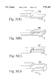
- FIGS. 5(A) to 5(D) are perspective, schematic diagrams that show alternative suspension structures according to the invention.
- FIGS. 6(A) to 6(D) provide a series of diagrams that show one example of reading and writing with a probing device according to the invention.
- FIG. 7(A) to 7(D) provide a series of diagrams that show another example of reading and writing with a probing device according to the invention.
- the invention provides a probing device that can significantly reduce the wear of the micro-needle caused by contact between the micro-needle on the probe tip and the surface of the probe target.
- the invention also provides a memory device having movable media that uses the probing device as the read/write mechanism.
- the wear of the micro-needle can be reduced by decreasing:
- atomic force microscope FAM
- a probe having a small spring constant and a needle having a small radius of curvature at the tip of the micro-needle are used, the external force applied by the probe, and the adsorption force and friction force of the micro-needle and substrate all decrease. Accordingly, the wear of the micro-needle is significantly reduced.
- the invention focuses on the large dependence of the wear of the micro-needle, on the effective inertial force (or the effective weight added to the micro-needle) of the probe and the micro-needle, regardless of the external force applied by the probe, and on the adsorption force and friction force of the micro-needle and substrate.
- the micro-needle and the probe are connected via a material that has a spring constant per unit length that is smaller than that of the probe body, the effective inertial force of the probe is decreased and the wear of the micro-needle is reduced.
- the inertial force is thought to be proportional to the square of the probe scanning speed in the horizontal direction. Therefore, when the needle scans at a high speed, the micro-needle collides with the probe target (sample) and the possibility of wear increases. In an AFM, the scanning speed is several ⁇ m/sec at the most. In a memory device having movable media, scanning at a speed higher than that of an AFM is preferred, but the wear of the micro-needle becomes the barrier, and a satisfactory scanning speed is not obtained. However, the inventors herein have found that if the effective inertial force of the micro-needle can be reduced as described above, the scanning speed can be significantly increased.
- the micro-needle at the probe tip does not always need to be in contact with the media or at a constant contact force.
- the probe moves at a constant speed with respect to the recording medium.
- the 1-bit memory cells that are recorded on the surface of the recording medium are formed at a constant pitch on the surface of the recording medium.
- the micro-needle only needs to access the memory medium periodically.
- the inventors herein have also discovered that if oscillations at a specific frequency are applied to the probe, so that the micro-needle is always or intermittently in contact with the surface of the probe target, then the wear of the needle is greatly reduced.
- the oscillation period of the probe can be synchronized to the access period for the memory medium by the micro-needle.
- the probing device comprises a cantilever-shaped probe having a micro-needle at its tip and an electric circuit that applies electrical signals between the micro-needle and the probe target (specifically, some electrical stimulus is applied to the probe target).
- a suspension with a spring constant per unit length that is less than that of the probe body is provided, and the micro-needle is formed on the suspension member (hereinafter, the probing device is referred to as a buffered probing device).
- a plate that is thinner than the probe body is used as the suspension member. Because the spring constant is proportional to the cube of its thickness, the spring constant can be easily lowered. For example, a plate that is thinner than the probe body can be folded to provide the suspension member (as discussed in greater detail below). Further, the suspension member is not limited to a plate configuration. For example, a frame shape or a bar shape can also be used for the suspension member. The suspension member is usually formed of the same material as that of the probe body.
- a circuit i.e. a probe control circuit for controlling the distance between the micro-needle and the probe target can be installed in the buffered probing device.
- Such distance control can be accomplished by the use of electrostatic force or piezoelectric force.
- a first electrode can be installed in the probe, and a second electrode can be installed on at least the substrate holding the probe or the substrate on the side where the probe target is located.
- the probing device is further comprised of a cantilever-shaped probe having a micro-needle formed on its tip, an electric circuit that applies electrical signals between the micro-needle and the probe target, and an excitation control circuit that applies oscillations at a specified frequency to the probe (hereinafter referred to as an excited probing device).
- Periodic oscillation of the probe can be generated by electrostatic force or by piezoelectric force.
- a first electrode and a second electrode are used as described above in connection with the buffered probing circuit.
- the electrostatic force is periodically generated between the first and second electrodes by the excitation control circuit (usually located in the probe control circuit), and oscillations at a specific frequency are applied to the probe.
- the probing device may also be provided as a combination of the buffered probing device and the excited probing device (hereinafter referred to as a buffered/excited probing device).
- the buffered/excited probing device is comprised of a cantilever-shaped probe that has a micro-needle in its tip, an electric circuit that applies electrical signals between the micro-needle and the probe target, a suspension in which the spring constant per unit length is less than that of the probe body, where the micro-needle formed in the suspension, and an excitation control circuit that applies oscillations at a specific frequency to the probe.
- a probe scanning mechanism can be included in the buffered, excited, and buffered/excited probing devices described above to move the probe and the probe target relative to each other along the surface of the probe target.
- the probe control circuit usually moves the micro-needle relative to the probe target while the micro-needle is in contact with the probe target. Because the effective mass of the probe tip is small, wear of the micro-needle is eliminated or decreased, even when the micro-needle collides with undulations on the surface of the probe target.
- the micro-needle When the micro-needle is moved relative to the probe target while the micro-needle is not in contact with the target, the micro-needle still collides with the undulations on the surface of the probe target. Wear on the micro-needle is nonetheless eliminated or reduced by the invention.
- a probe control circuit in an excited probing device or a buffered/excited probing device :
- the electrical signals i.e. electrical stimulus applied to the probe target
- the electrical signals may or may not be synchronized to the probe oscillations.
- the contact needle and the probe target are separated.
- the micro-needle cannot always apply the electrical stimulus to the probe target.
- the timing at which the electrical stimulus is applied must be synchronized to the timing at which the micro-needle gets close to or touches the probe target.
- Buffered and excited probing devices or a buffered/excited probing device can be used to measure the surface of the probe target.
- the invention is readily applied to the read/write mechanism for a memory device having movable media.
- a recording medium that can read and write data is used as the probe target, and the data read or write signals are used as the electrical signals.
- FIG. 1 shows one example of the structure of the buffered/excited probing device according to the invention.
- the cantilever-shaped probe 1 in the probe support substrate 2 is configured so as to project outwardly to the surface of the recording medium 3.
- the probe 1 becomes a three-layered structure consisting of conductive layers 12, 13 laminated to both sides of an insulating layer 11.
- a thin suspension member 9 is formed on the probe tip 1 where the top of the probe 1 is cut out.
- a micro-needle 4 is formed facing the recording medium on the side of the probe with the conductive layer 13 on the tip of the suspension member 9.
- a movable electrode 51 having a large area is formed on the side of the probe with conductive layer 12 on the tip of the probe 1 parallel to the surface of the recording medium 3.
- the recording medium 3 becomes a two-layered structure of the recording layer 31 and the medium electrode 32.
- the recording layer 31 is positioned on the side of the medium facing the probe 1.
- the recording layer 31 is made from a dielectric material, and the medium electrode 32 is made from conductive material.
- a probe control circuit 6 is connected between the movable electrode 51 and the medium layer 32.
- the probe control circuit 6 includes a series circuit consisting of a bias supply 61 and a modulation source 62.
- An electric circuit 7 for reading/writing is connected between the conductive layer 12 and the medium layer 32, i.e. between the micro-needle 4 and the medium electrode 32).
- the probe support substrate 2 does not move, and the recording medium 3 moves in the X-Y direction. This movement is performed by the probe scanning mechanism 8.
- a specified voltage (modulation voltage V m ) is applied between the movable electrode 51 and the medium electrode 32 by the probe control circuit 6.
- the voltage V m is a periodic signal, such as a sequence of pulses.
- An electrostatic attractive force between the movable electrode 51 and the medium electrode 32 is generated with a constant period, i.e. oscillations having a specific frequency are applied to the movable electrode 51.
- the frequency of the signal generated by the modulation source 62 is determined by probe 1 structure, e.g. shape and material in each structural element. For example, the signal frequency can be matched to the resonance frequency of probe 1.
- the suspension member 9 has a high characteristic resonance frequency with respect to the body of the probe 1. Consequently, the frequency of the signal applied by the probe control circuit 6 can be matched to this resonance frequency.
- the buffered/excited probing device can be built using monolithic silicon lamination technology.
- the length L of probe 1 is about 40 ⁇ m; the width W is about 4 ⁇ m; and the thickness T is about 0.3 ⁇ m.
- the length L E and width W E of the movable electrode are about 5 ⁇ m; the diameter D N and height H N of the micro-needle are each about 100 nm.
- the length L s of the suspension 9 is preferably about 2 ⁇ m and the thickness is preferably about 0.1 ⁇ m.
- FIG. 2 shows another structural example of the buffered/excited probing device.
- FIG. 3 is the cross-sectional view of the buffered/excited probing device of FIG. 2, taken in the A--A direction.
- a pair of fixed electrodes 52, 53 and one movable electrode 51 are shown.
- the probing device shown in FIG. 2 differs from the probing device shown in FIG. 1.
- oscillations are applied to probe 1.
- the fixed electrode 53 is installed on top of the movable electrode 51 (side where the micro-needle 4 is not formed).
- the fixed electrode 52 is installed below the movable electrode 51 (side where micro-needle 4 is formed).
- a probe control circuit 6 is connected between the movable electrode 51 and the fixed electrodes 52, 53.
- a bias supply 63 is connected between the fixed electrodes 52 and 53.
- a DC circuit of the bias supply 61 generates a bias that is less than that of the bias supply 63.
- a modulation source 62 is connected between the movable electrode 51 and the fixed electrode 53.
- the movable electrode 51 can receive electrostatic force from the fixed electrodes 52 and 53. Accordingly, the movable electrode 51 can be controlled with high reliability. Also, the area of the movable electrode 51 can be smaller than that shown for the embodiment of FIG. 1.
- an electrode that corresponds to the fixed electrode 53 (shown in FIG. 2) can be installed on the probe 1 side.
- a probe control circuit 6 with the structure shown in FIG. 2 is used.
- the fixed electrode 53 can be omitted.
- a probe control circuit 6 having the structure shown in FIG. 1 is used.
- FIG. 4 shows another example structure of the buffered/excited probing device.
- the probing device shown in FIG. 4 has a movable electrode 51 installed in the center of the probe 1.
- the micro-needle 4 is separated from the movable electrode 51, the effective inertial force at the tip of the probe 1 is small compared to that of the structures shown in FIGS. 1 and 2.
- FIGS. 5(A) to 5(D) show other example structures for the suspension member.
- the suspension member 9A shown in FIG. 5(A) is thinner than the body of the probe 1 and is installed to project downward.
- the advantage of this suspension member is that the distance between the micro-needle 4 and the body of the probe 1 increases.
- the suspension member 9B shown in FIG. 5(B) has a frame form from which the center part of the suspension member 9 shown in FIG. 1 has been removed.
- the suspension member 9B is thinner than the body of the probe 1, but can have the same thickness as the body of the probe 1, as shown by the dashed lines.
- the suspension member 90 shown in FIG. 5(C) has a bar shape from which both sides of the suspension member 9 shown in FIG. 1 have been removed.
- the suspension member is thinner than the body of the probe 1, but can have the same thickness as the body of the probe 1, as shown by the dashed lines.
- the suspension member 9D shown in FIG. 5(D) is formed as a plate that is thinner than the body of the probe 1 and is folded downward. In FIG. 5(D), a bend that corresponds to the force received from the recording medium can become large in a short length (i.e. the effective inertial force of the micro-needle 4 becomes small).
- the following describes data reading and writing for a memory device having movable media that uses the buffered/excited probing device.
- the probe 1 By driving the modulation source 62 of the probe control circuit 6, the probe 1 starts oscillating. Such oscillation quickly enters a steady state. The time until the oscillation moves to a steady state is determined by the lengths, thicknesses, widths, and materials of the probe 1 and suspension member 9. Usually, the time is very short.
- the oscillation center of the probe 1 is set to correspond to the supply voltage of the bias supply (numeric designator 61 in the probing device shown in FIG. 1; numeric designators 61 and 63 in the probing device shown in FIG. 2).
- the probe 1 oscillates and scans, as explained below with reference to FIGS. 6(A) to 6(D).
- the memory medium 3 is moved rapidly with respect to the probe 1.
- FIGS. 6(A) and 6(B) show the relationship between the force F e applied through probe 1 at the tip of the micro-needle 2 and the contact force F c at tip of the micro-needle 4 along the time axis (t).
- Force F e has the same characteristics as the signal waveform of the modulation source 62.
- Force F c is the vector sum of the resistance force that opposes external forces, adsorption force (intermolecular attractive force between the molecules at the tip of the micro-needle 4 and the molecules that form the recording medium), frictional force, and inertial force of the probe.
- force F e becomes less than zero in no more than one period. Even when a period where force F e is less than zero exists, the micro-needle is not separated from the recording medium 3.
- the magnitude of the contact force F c usually has a value greater than zero.
- FIG. 6(C) shows the appearance of the surface of the recording medium 3 for the elapsed time and the micro-needle 4. Pulses are applied to the recording medium 3 by the electric circuit for reading and writing.
- FIG. 6(D) shows the pulses for reading and writing and corresponds to FIGS. 6(A) to 6(C).
- the micro-needle 4 is always in contact with the surface of the recording medium. Therefore, read/write timing must not match the timing where the contact force F c reaches a maximum.
- the read/write period can be greater or less than the oscillation period of the probe 1. As shown in FIG. 6(D), the read/write period can be synchronized to the oscillation period of the probe.
- the suspension member 9 is placed between the probe 1 and the micro-needle 4. Because the suspension member 9 is subject to a significant amount of bending when the micro-needle 4 is in contact with the undulations on the surface of the recording medium 3, even for a small force, wear on the micro-needle 4 is eliminated or reduced.
- FIGS. 7(A) to 7(D) With reference to FIGS. 7(A) to 7(D), the case where the micro-needle 4 is repeatedly in contact and not in contact with the medium 3 at a specified frequency is explained. Because FIGS. 7(A) to 7(D) are analogous to FIGS. 6(A) to 6(D), respectively, detailed explanations of the figures are omitted. The definitions of force F e and force F c in FIG. 7 are also the same as the definitions in FIG. 6 and are omitted.
- the period where force F e is less than zero is long.
- the micro-needle separates from the recording medium.
- the loci of the micro-needle 4 are written side by side in FIG. 7(C).
- the read/write timing as shown in FIG. 7(D) is synchronized to the timing where the contact force F c becomes a maximum.
- the read/write period can be greater than or less than the oscillation period of the probe 1. Because writing or reading is possible even during the period in which the micro-needle is not in contact with the recording medium, the read/write timing is not limited to the timing that is shown in FIG. 7(D). Furthermore, in the buffered/excited probing device the scanning speed (i.e. the moving speed of the memory medium) during normal use may be doubled and a mode for high-speed reading of data is possible.
- the suspension member 9 bends a great deal even for a small force.
- wear on the micro-needle 4 is eliminated or reduced.
- a buffered/excited probing device is described above, a buffered probing device or an excited probing device can be used in the read/write mechanism of a scanning memory device.
- reading or writing may be performed either with the micro-needle 4 is always in contact with the recording medium 3 or with the micro-needle never in contact with the recording medium.
- oscillation cannot be applied to the probe 1.
- the modulation source is not installed in the probe control circuit.
- the distance between the micro-needle 4 and recording medium 3 is several angstroms ( ⁇ ).
- ⁇ angstroms
- the suspension member 9 cannot be formed on the tip of the probe 1. Even when the suspension 9 is not formed on the tip of the probe 1, the mechanism of the excited probing device is similar to that of the buffered/excited probing device.
- the frequency of the signal that generates the modulation source 62 matches the resonance frequency of the probe 1, the drive consumption current of the control circuit is small. To obtain the oscillation of the stable probe 1, applying a frequency that is less than the resonance frequency of the probe 1 is preferred.
- the probing device can be used as a read/write mechanism, and the wear life of the micro-needle is significantly extended. Furthermore, because the distance between the micro-needle and the surface of the probe target does not have to be detected, a more compact device can be designed, and its production cost can be decreased without making the peripheral circuits more complex.
Landscapes
- Measuring Leads Or Probes (AREA)
- Length Measuring Devices With Unspecified Measuring Means (AREA)
Applications Claiming Priority (2)
| Application Number | Priority Date | Filing Date | Title |
|---|---|---|---|
| JP7155222A JPH08329538A (ja) | 1995-05-30 | 1995-05-30 | プローブ装置 |
| JP7/155222 | 1995-05-30 |
Publications (1)
| Publication Number | Publication Date |
|---|---|
| US5751685A true US5751685A (en) | 1998-05-12 |
Family
ID=15601201
Family Applications (1)
| Application Number | Title | Priority Date | Filing Date |
|---|---|---|---|
| US08/644,385 Expired - Fee Related US5751685A (en) | 1995-05-30 | 1996-05-10 | Probe for memory device having movable media |
Country Status (3)
| Country | Link |
|---|---|
| US (1) | US5751685A (ja) |
| EP (1) | EP0745987A3 (ja) |
| JP (1) | JPH08329538A (ja) |
Cited By (35)
| Publication number | Priority date | Publication date | Assignee | Title |
|---|---|---|---|---|
| US5932876A (en) * | 1996-10-24 | 1999-08-03 | Centre Suisse E'electronique Et De Microtechnique S.A. | Tunnel effect sensor, suitable for determining the topography of a surface |
| US5953306A (en) * | 1996-04-25 | 1999-09-14 | Hewlett-Packard Company | Micro needle probe apparatus having probes cantilevered over respective electronic circuits, moving medium memory device including same and method of making same |
| US20030053400A1 (en) * | 2001-09-10 | 2003-03-20 | Yasuo Cho | Dielectric information apparatus, tape-like medium recording/reproducing apparatus and disc-like medium recording/reproducing apparatus |
| US20030202456A1 (en) * | 2002-04-25 | 2003-10-30 | Samsung Electronics Co., Ltd. | Apparatus and method for reproducing data using capacitance variation |
| US20040027935A1 (en) * | 2002-06-06 | 2004-02-12 | Yasuo Cho | Dielectric recording/reproducing head, dielectric recording medium unit, and dielectric recording/reproducing apparatus |
| US20040042351A1 (en) * | 2002-07-09 | 2004-03-04 | Pioneer Corporation | Dielectric recording / reproducing head and tracking mothod |
| US20040047245A1 (en) * | 2002-07-09 | 2004-03-11 | Stsushi Onoe | Pickup device |
| US20040090903A1 (en) * | 2002-09-11 | 2004-05-13 | Yasuo Cho And Pioneer Corporation | Dielectric recording apparatus, dielectric reproducing apparatus, and dielectric recording / reproducing apparatus |
| US20040145941A1 (en) * | 2002-10-15 | 2004-07-29 | Rust Thomas F | Phase change media for high density data storage |
| US20040145848A1 (en) * | 2002-10-15 | 2004-07-29 | Rust Thomas F. | Molecular memory integrated circuit utilizing non-vibrating cantilevers |
| US20040150472A1 (en) * | 2002-10-15 | 2004-08-05 | Rust Thomas F. | Fault tolerant micro-electro mechanical actuators |
| US20040246879A1 (en) * | 2002-07-09 | 2004-12-09 | Atsushi Onoe | Recording/reproducing head and method of producing the same |
| US20040252621A1 (en) * | 2003-06-12 | 2004-12-16 | Yasuo Cho | Data recording / reproducing apparatus and method using needle-shaped member |
| US20040263185A1 (en) * | 2001-09-10 | 2004-12-30 | Yasuo Cho | Dielectric constant measuring apparatus, dielectric constant measuring method, and information recording/reproducing apparatus |
| US20050099895A1 (en) * | 2003-11-06 | 2005-05-12 | Pioneer Corporation | Information recording/reproducing apparatus and recording medium |
| US20050135203A1 (en) * | 2003-12-17 | 2005-06-23 | Hewlett-Packard Development Co. | Contact probe storage sensor pod |
| US20050147017A1 (en) * | 2004-01-07 | 2005-07-07 | Hewlett-Packard Development Co. L.P. | Data readout arrangement |
| US20050232004A1 (en) * | 2004-04-16 | 2005-10-20 | Rust Thomas F | Methods for erasing bit cells in a high density data storage device |
| US20050232061A1 (en) * | 2004-04-16 | 2005-10-20 | Rust Thomas F | Systems for writing and reading highly resolved domains for high density data storage |
| US20070006455A1 (en) * | 2005-06-24 | 2007-01-11 | Nanochip, Inc. | Methods for forming high density data storage devices with read/write probes with hollow or reinforced tips |
| US20070010054A1 (en) * | 2005-07-08 | 2007-01-11 | Nanochip, Inc. | Method for forming patterned media for a high density data storage device |
| US20070014047A1 (en) * | 2003-05-01 | 2007-01-18 | Yasuo Cho | Recording/reproduction head and recording/reproduction device |
| US20070070685A1 (en) * | 2002-10-15 | 2007-03-29 | Rust Thomas F | Atomic probes and media for high density data storage |
| US7212488B2 (en) | 2005-03-21 | 2007-05-01 | Hewlett-Packard Development Company, L.P. | Method and device enabling capacitive probe-based data storage readout |
| US20070154354A1 (en) * | 2001-09-12 | 2007-07-05 | Faris Sadeg M | Probes and methods of making probes using folding techniques |
| US7260051B1 (en) | 1998-12-18 | 2007-08-21 | Nanochip, Inc. | Molecular memory medium and molecular memory integrated circuit |
| US20080035583A1 (en) * | 2003-08-22 | 2008-02-14 | Lopez Martinez Josem | Methods, Devices and Reagents for Wastewater Treatment |
| US7336590B2 (en) | 2002-09-11 | 2008-02-26 | Yasuo Cho | Dielectric reproducing apparatus, dielectric recording apparatus, and dielectric recording/reproducing apparatus |
| US7379412B2 (en) | 2004-04-16 | 2008-05-27 | Nanochip, Inc. | Methods for writing and reading highly resolved domains for high density data storage |
| EP1422707A3 (en) * | 2002-11-18 | 2008-09-10 | Pioneer Corporation | Information recording / reading head |
| US7436753B2 (en) | 2003-12-17 | 2008-10-14 | Mejia Robert G | Contact probe storage FET sensor |
| US7463573B2 (en) | 2005-06-24 | 2008-12-09 | Nanochip, Inc. | Patterned media for a high density data storage device |
| US20080316904A1 (en) * | 2007-05-10 | 2008-12-25 | Duerig Urs T | Method and apparatus for reducing tip-wear of a probe |
| US20090010144A1 (en) * | 2007-07-02 | 2009-01-08 | Seagate Technology Llc | Transducer Assembly and Data Storage Apparatus Including the Transducer Assembly |
| US7590040B2 (en) | 2003-08-25 | 2009-09-15 | Yasuo Cho | Signal detecting method and apparatus and information reproducing apparatus and method |
Families Citing this family (2)
| Publication number | Priority date | Publication date | Assignee | Title |
|---|---|---|---|---|
| US6445106B1 (en) * | 2000-02-18 | 2002-09-03 | Intel Corporation | Micro-electromechanical structure resonator, method of making, and method of using |
| KR100519752B1 (ko) | 2002-05-10 | 2005-10-07 | 삼성전자주식회사 | 시분할 다중 방식을 채용한 고속 고밀도 정보저장 장치 및이를 이용한 정보기록방법 및 정보재생방법 |
Citations (6)
| Publication number | Priority date | Publication date | Assignee | Title |
|---|---|---|---|---|
| US5086409A (en) * | 1984-11-30 | 1992-02-04 | Canon Kabushiki Kaisha | Recording and/or reproducing method of bloch line memory |
| US5418363A (en) * | 1992-11-30 | 1995-05-23 | Digital Instruments, Inc. | Scanning probe microscope using stored data for vertical probe positioning |
| US5461605A (en) * | 1991-07-17 | 1995-10-24 | Canon Kabushiki Kaisha | Information recording/reproducing method, recording carrier and apparatus for recording and/or reproducing information on information recording carrier by use of probe electrode |
| US5506829A (en) * | 1990-12-17 | 1996-04-09 | Canon Kabushiki Kaisha | Cantilever probe and apparatus using the same |
| US5526334A (en) * | 1992-12-24 | 1996-06-11 | Canon Kabushiki Kaisha | Information processing apparatus with multiple probes and method therefor |
| US5546374A (en) * | 1993-09-29 | 1996-08-13 | Canon Kabushiki Kaisha | Information recording and/or reproducing apparatus using probe |
Family Cites Families (10)
| Publication number | Priority date | Publication date | Assignee | Title |
|---|---|---|---|---|
| US3706861A (en) * | 1969-09-18 | 1972-12-19 | Rca Corp | Apparatus for mounting and spacing a signal transducer with respect to a recording medium |
| US3632900A (en) * | 1969-12-31 | 1972-01-04 | Ibm | Magnetic transducer displacement control system |
| JPS57141040A (en) * | 1981-02-24 | 1982-09-01 | Toshiba Corp | Recording and reproducing decive |
| JPH029068A (ja) * | 1988-06-27 | 1990-01-12 | Nippon Telegr & Teleph Corp <Ntt> | 記録及び/又は再生方法 |
| JP3030574B2 (ja) * | 1990-08-16 | 2000-04-10 | キヤノン株式会社 | 微小変位型情報検知探針素子及びこれを用いた走査型トンネル顕微鏡、原子間力顕微鏡、情報処理装置 |
| US5216631A (en) * | 1990-11-02 | 1993-06-01 | Sliwa Jr John W | Microvibratory memory device |
| JPH04345928A (ja) * | 1991-05-24 | 1992-12-01 | Sony Corp | 記録媒体ディスクのドライブ装置 |
| DE4211813C1 (en) * | 1992-04-08 | 1993-06-09 | Forschungszentrum Juelich Gmbh, 5170 Juelich, De | Electronic spacing regulation circuit for resonating test probe - provides piezoelectric position adjustment dependent on phase difference between detected oscillation and reference oscillation |
| US5400647A (en) * | 1992-11-12 | 1995-03-28 | Digital Instruments, Inc. | Methods of operating atomic force microscopes to measure friction |
| JPH0763999A (ja) * | 1993-08-27 | 1995-03-10 | Canon Inc | 静電アクチュエータ、該静電アクチュエータを備えたアクチュエータアレイ、光偏向器および情報処理装置 |
-
1995
- 1995-05-30 JP JP7155222A patent/JPH08329538A/ja active Pending
-
1996
- 1996-05-10 US US08/644,385 patent/US5751685A/en not_active Expired - Fee Related
- 1996-05-15 EP EP96303453A patent/EP0745987A3/en not_active Withdrawn
Patent Citations (7)
| Publication number | Priority date | Publication date | Assignee | Title |
|---|---|---|---|---|
| US5086409A (en) * | 1984-11-30 | 1992-02-04 | Canon Kabushiki Kaisha | Recording and/or reproducing method of bloch line memory |
| US5506829A (en) * | 1990-12-17 | 1996-04-09 | Canon Kabushiki Kaisha | Cantilever probe and apparatus using the same |
| US5461605A (en) * | 1991-07-17 | 1995-10-24 | Canon Kabushiki Kaisha | Information recording/reproducing method, recording carrier and apparatus for recording and/or reproducing information on information recording carrier by use of probe electrode |
| US5418363A (en) * | 1992-11-30 | 1995-05-23 | Digital Instruments, Inc. | Scanning probe microscope using stored data for vertical probe positioning |
| US5418363B1 (en) * | 1992-11-30 | 1998-01-06 | Digital Instr Inc | Scanning probe microscope using stored data for vertical probe positioning |
| US5526334A (en) * | 1992-12-24 | 1996-06-11 | Canon Kabushiki Kaisha | Information processing apparatus with multiple probes and method therefor |
| US5546374A (en) * | 1993-09-29 | 1996-08-13 | Canon Kabushiki Kaisha | Information recording and/or reproducing apparatus using probe |
Non-Patent Citations (2)
| Title |
|---|
| Tamanuki, Takemasa et al., "Temperature Characteristics of Short-Cavity AlGaAs/GaAs Surface Emitting Lasers", IEICE Transactions, vol. E 74, No. 11, pp. 3867-3869. |
| Tamanuki, Takemasa et al., Temperature Characteristics of Short Cavity AlGaAs/GaAs Surface Emitting Lasers , IEICE Transactions, vol. E 74, No. 11, pp. 3867 3869. * |
Cited By (55)
| Publication number | Priority date | Publication date | Assignee | Title |
|---|---|---|---|---|
| US5953306A (en) * | 1996-04-25 | 1999-09-14 | Hewlett-Packard Company | Micro needle probe apparatus having probes cantilevered over respective electronic circuits, moving medium memory device including same and method of making same |
| US5932876A (en) * | 1996-10-24 | 1999-08-03 | Centre Suisse E'electronique Et De Microtechnique S.A. | Tunnel effect sensor, suitable for determining the topography of a surface |
| US7260051B1 (en) | 1998-12-18 | 2007-08-21 | Nanochip, Inc. | Molecular memory medium and molecular memory integrated circuit |
| US7391707B2 (en) | 1998-12-18 | 2008-06-24 | Nanochip, Inc. | Devices and methods of detecting movement between media and probe tip in a probe data storage system |
| US20030053400A1 (en) * | 2001-09-10 | 2003-03-20 | Yasuo Cho | Dielectric information apparatus, tape-like medium recording/reproducing apparatus and disc-like medium recording/reproducing apparatus |
| US7218600B2 (en) | 2001-09-10 | 2007-05-15 | Pioneer Corporation | Dielectric constant measuring apparatus, dielectric constant measuring method, and information recording/reproducing apparatus |
| US7242661B2 (en) * | 2001-09-10 | 2007-07-10 | Pioneer Corporation | Dielectric information apparatus, tape-like medium recording/reproducing apparatus and disc-like medium recording/reproducing apparatus |
| US20040263185A1 (en) * | 2001-09-10 | 2004-12-30 | Yasuo Cho | Dielectric constant measuring apparatus, dielectric constant measuring method, and information recording/reproducing apparatus |
| US20070154354A1 (en) * | 2001-09-12 | 2007-07-05 | Faris Sadeg M | Probes and methods of making probes using folding techniques |
| US7765607B2 (en) * | 2001-09-12 | 2010-07-27 | Faris Sadeg M | Probes and methods of making probes using folding techniques |
| US20030202456A1 (en) * | 2002-04-25 | 2003-10-30 | Samsung Electronics Co., Ltd. | Apparatus and method for reproducing data using capacitance variation |
| US20040027935A1 (en) * | 2002-06-06 | 2004-02-12 | Yasuo Cho | Dielectric recording/reproducing head, dielectric recording medium unit, and dielectric recording/reproducing apparatus |
| US7283453B2 (en) * | 2002-07-09 | 2007-10-16 | Pioneer Corporation | Recording/reproducing head |
| US7221639B2 (en) | 2002-07-09 | 2007-05-22 | Pioneer Corporation | Pickup device |
| US20040042351A1 (en) * | 2002-07-09 | 2004-03-04 | Pioneer Corporation | Dielectric recording / reproducing head and tracking mothod |
| US20040246879A1 (en) * | 2002-07-09 | 2004-12-09 | Atsushi Onoe | Recording/reproducing head and method of producing the same |
| US20040047245A1 (en) * | 2002-07-09 | 2004-03-11 | Stsushi Onoe | Pickup device |
| US20040090903A1 (en) * | 2002-09-11 | 2004-05-13 | Yasuo Cho And Pioneer Corporation | Dielectric recording apparatus, dielectric reproducing apparatus, and dielectric recording / reproducing apparatus |
| US7227830B2 (en) | 2002-09-11 | 2007-06-05 | Yasuo Cho | Dielectric recording apparatus, dielectric reproducing apparatus, and dielectric recording / reproducing apparatus |
| US7336590B2 (en) | 2002-09-11 | 2008-02-26 | Yasuo Cho | Dielectric reproducing apparatus, dielectric recording apparatus, and dielectric recording/reproducing apparatus |
| US7336524B2 (en) | 2002-10-15 | 2008-02-26 | Nanochip, Inc. | Atomic probes and media for high density data storage |
| US7233517B2 (en) | 2002-10-15 | 2007-06-19 | Nanochip, Inc. | Atomic probes and media for high density data storage |
| US20040145941A1 (en) * | 2002-10-15 | 2004-07-29 | Rust Thomas F | Phase change media for high density data storage |
| US20070070685A1 (en) * | 2002-10-15 | 2007-03-29 | Rust Thomas F | Atomic probes and media for high density data storage |
| US6985377B2 (en) | 2002-10-15 | 2006-01-10 | Nanochip, Inc. | Phase change media for high density data storage |
| US6982898B2 (en) | 2002-10-15 | 2006-01-03 | Nanochip, Inc. | Molecular memory integrated circuit utilizing non-vibrating cantilevers |
| US20040145848A1 (en) * | 2002-10-15 | 2004-07-29 | Rust Thomas F. | Molecular memory integrated circuit utilizing non-vibrating cantilevers |
| US20040150472A1 (en) * | 2002-10-15 | 2004-08-05 | Rust Thomas F. | Fault tolerant micro-electro mechanical actuators |
| EP1422707A3 (en) * | 2002-11-18 | 2008-09-10 | Pioneer Corporation | Information recording / reading head |
| US20070014047A1 (en) * | 2003-05-01 | 2007-01-18 | Yasuo Cho | Recording/reproduction head and recording/reproduction device |
| US20040252621A1 (en) * | 2003-06-12 | 2004-12-16 | Yasuo Cho | Data recording / reproducing apparatus and method using needle-shaped member |
| US7385901B2 (en) | 2003-06-12 | 2008-06-10 | Yasuo Cho | Data recording/reproducing apparatus and method using needle-shaped member |
| US8004948B2 (en) | 2003-06-12 | 2011-08-23 | Yasuo Cho | Data recording / reproducing apparatus and method using needle-shaped member |
| US20080035583A1 (en) * | 2003-08-22 | 2008-02-14 | Lopez Martinez Josem | Methods, Devices and Reagents for Wastewater Treatment |
| US7590040B2 (en) | 2003-08-25 | 2009-09-15 | Yasuo Cho | Signal detecting method and apparatus and information reproducing apparatus and method |
| US20050099895A1 (en) * | 2003-11-06 | 2005-05-12 | Pioneer Corporation | Information recording/reproducing apparatus and recording medium |
| US7436753B2 (en) | 2003-12-17 | 2008-10-14 | Mejia Robert G | Contact probe storage FET sensor |
| US20050135203A1 (en) * | 2003-12-17 | 2005-06-23 | Hewlett-Packard Development Co. | Contact probe storage sensor pod |
| US7423954B2 (en) | 2003-12-17 | 2008-09-09 | Hewlett-Packard Development Company, L.P. | Contact probe storage sensor pod |
| US20050147017A1 (en) * | 2004-01-07 | 2005-07-07 | Hewlett-Packard Development Co. L.P. | Data readout arrangement |
| US7212487B2 (en) | 2004-01-07 | 2007-05-01 | Hewlett-Packard Development Company, L.P. | Data readout arrangement |
| US7379412B2 (en) | 2004-04-16 | 2008-05-27 | Nanochip, Inc. | Methods for writing and reading highly resolved domains for high density data storage |
| US20050232004A1 (en) * | 2004-04-16 | 2005-10-20 | Rust Thomas F | Methods for erasing bit cells in a high density data storage device |
| US7414953B2 (en) | 2004-04-16 | 2008-08-19 | Nanochip, Inc. | Memory having a layer with electrical conductivity anisotropy |
| US20050232061A1 (en) * | 2004-04-16 | 2005-10-20 | Rust Thomas F | Systems for writing and reading highly resolved domains for high density data storage |
| US7301887B2 (en) | 2004-04-16 | 2007-11-27 | Nanochip, Inc. | Methods for erasing bit cells in a high density data storage device |
| US7212488B2 (en) | 2005-03-21 | 2007-05-01 | Hewlett-Packard Development Company, L.P. | Method and device enabling capacitive probe-based data storage readout |
| US20070006455A1 (en) * | 2005-06-24 | 2007-01-11 | Nanochip, Inc. | Methods for forming high density data storage devices with read/write probes with hollow or reinforced tips |
| US7367119B2 (en) | 2005-06-24 | 2008-05-06 | Nanochip, Inc. | Method for forming a reinforced tip for a probe storage device |
| US7463573B2 (en) | 2005-06-24 | 2008-12-09 | Nanochip, Inc. | Patterned media for a high density data storage device |
| US7309630B2 (en) | 2005-07-08 | 2007-12-18 | Nanochip, Inc. | Method for forming patterned media for a high density data storage device |
| US20070010054A1 (en) * | 2005-07-08 | 2007-01-11 | Nanochip, Inc. | Method for forming patterned media for a high density data storage device |
| US20080316904A1 (en) * | 2007-05-10 | 2008-12-25 | Duerig Urs T | Method and apparatus for reducing tip-wear of a probe |
| US8023393B2 (en) * | 2007-05-10 | 2011-09-20 | International Business Machines Corporation | Method and apparatus for reducing tip-wear of a probe |
| US20090010144A1 (en) * | 2007-07-02 | 2009-01-08 | Seagate Technology Llc | Transducer Assembly and Data Storage Apparatus Including the Transducer Assembly |
Also Published As
| Publication number | Publication date |
|---|---|
| JPH08329538A (ja) | 1996-12-13 |
| EP0745987A2 (en) | 1996-12-04 |
| EP0745987A3 (en) | 1997-02-26 |
Similar Documents
| Publication | Publication Date | Title |
|---|---|---|
| EP0745987A2 (en) | Probe for memory device having movable media | |
| CA1275503C (en) | Micro mechanical actual transducer head on a slider | |
| JP3157840B2 (ja) | 新規なカンチレバー構造 | |
| US7391707B2 (en) | Devices and methods of detecting movement between media and probe tip in a probe data storage system | |
| US4843502A (en) | Magnetic head slider loading mechanism for magnetic disk apparatus | |
| KR100600930B1 (ko) | 레코더, 플레이어, 정보 저장 및 판독 방법 | |
| JPH0534748B2 (ja) | ||
| EP0729006B1 (en) | Information processing apparatus with probe undergoing circular motion | |
| JPH0518741A (ja) | 微小変位型情報検知探針素子及びこれを用いた走査型トンネル顕微鏡、原子間力顕微鏡、情報処理装置 | |
| US5444191A (en) | Information processing apparatus and device for use in same | |
| US7464584B2 (en) | Semiconductor probe and method of writing and reading information using the same | |
| CN100411015C (zh) | 微驱动器、设有该微驱动器的磁头折片组合以及磁盘驱动器 | |
| KR100519752B1 (ko) | 시분할 다중 방식을 채용한 고속 고밀도 정보저장 장치 및이를 이용한 정보기록방법 및 정보재생방법 | |
| JP4095125B2 (ja) | メモリー装置 | |
| KR100331444B1 (ko) | 강유전체 박막을 이용한 초고밀도 정보 저장 장치 | |
| JP2001076443A (ja) | 電気機械変換素子を使用した駆動装置 | |
| JP4097632B2 (ja) | マルチプローブストレージ装置 | |
| JP2890268B2 (ja) | プローブユニット及びこれを用いた情報処理装置と走査型トンネル顕微鏡 | |
| JP4054049B2 (ja) | 強誘電性情報保存装置及び情報保存/再生方法 | |
| US6937418B2 (en) | Magnetic storage device having a head suspension supporting a head slider | |
| JPH05128459A (ja) | ヘツドアクチユエータ | |
| JPH06139629A (ja) | 情報記録坦体およびこれを使用する情報処理装置 | |
| JP2976703B2 (ja) | ヘッドアクチュエータ | |
| JPH07211035A (ja) | 磁気記録再生装置。 | |
| JPH0478037A (ja) | 記録再生装置及び記録再生消去方法 |
Legal Events
| Date | Code | Title | Description |
|---|---|---|---|
| AS | Assignment |
Owner name: HEWLETT-PACKARD COMPANY, A DELAWARE CORPORATION, C Free format text: MERGER;ASSIGNOR:HEWLETT-PACKARD COMPANY, A CALIFORNIA CORPORATION;REEL/FRAME:010841/0649 Effective date: 19980520 |
|
| AS | Assignment |
Owner name: AGILENT TECHNOLOGIES INC, CALIFORNIA Free format text: ASSIGNMENT OF ASSIGNORS INTEREST;ASSIGNOR:HEWLETT-PACKARD COMPANY;REEL/FRAME:010977/0540 Effective date: 19991101 |
|
| FPAY | Fee payment |
Year of fee payment: 4 |
|
| FEPP | Fee payment procedure |
Free format text: PAYOR NUMBER ASSIGNED (ORIGINAL EVENT CODE: ASPN); ENTITY STATUS OF PATENT OWNER: LARGE ENTITY |
|
| REMI | Maintenance fee reminder mailed | ||
| FPAY | Fee payment |
Year of fee payment: 8 |
|
| REMI | Maintenance fee reminder mailed | ||
| LAPS | Lapse for failure to pay maintenance fees | ||
| STCH | Information on status: patent discontinuation |
Free format text: PATENT EXPIRED DUE TO NONPAYMENT OF MAINTENANCE FEES UNDER 37 CFR 1.362 |
|
| FP | Lapsed due to failure to pay maintenance fee |
Effective date: 20100512 |