WO1984004825A1 - Materiau electrophotographique sensibilise - Google Patents
Materiau electrophotographique sensibilise Download PDFInfo
- Publication number
- WO1984004825A1 WO1984004825A1 PCT/JP1984/000256 JP8400256W WO8404825A1 WO 1984004825 A1 WO1984004825 A1 WO 1984004825A1 JP 8400256 W JP8400256 W JP 8400256W WO 8404825 A1 WO8404825 A1 WO 8404825A1
- Authority
- WO
- WIPO (PCT)
- Prior art keywords
- photosensitive material
- photosensitive
- derivative
- alkyl group
- group
- Prior art date
- Legal status (The legal status is an assumption and is not a legal conclusion. Google has not performed a legal analysis and makes no representation as to the accuracy of the status listed.)
- Ceased
Links
Classifications
-
- G—PHYSICS
- G03—PHOTOGRAPHY; CINEMATOGRAPHY; ANALOGOUS TECHNIQUES USING WAVES OTHER THAN OPTICAL WAVES; ELECTROGRAPHY; HOLOGRAPHY
- G03G—ELECTROGRAPHY; ELECTROPHOTOGRAPHY; MAGNETOGRAPHY
- G03G5/00—Recording-members for original recording by exposure, e.g. to light, to heat or to electrons; Manufacture thereof; Selection of materials therefor
- G03G5/02—Charge-receiving layers
- G03G5/04—Photoconductive layers; Charge-generation layers or charge-transporting layers; Additives therefor; Binders therefor
- G03G5/06—Photoconductive layers; Charge-generation layers or charge-transporting layers; Additives therefor; Binders therefor characterised by the photoconductive material being organic
- G03G5/0664—Dyes
- G03G5/0666—Dyes containing a methine or polymethine group
- G03G5/0668—Dyes containing a methine or polymethine group containing only one methine or polymethine group
- G03G5/067—Dyes containing a methine or polymethine group containing only one methine or polymethine group containing hetero rings
-
- G—PHYSICS
- G03—PHOTOGRAPHY; CINEMATOGRAPHY; ANALOGOUS TECHNIQUES USING WAVES OTHER THAN OPTICAL WAVES; ELECTROGRAPHY; HOLOGRAPHY
- G03G—ELECTROGRAPHY; ELECTROPHOTOGRAPHY; MAGNETOGRAPHY
- G03G5/00—Recording-members for original recording by exposure, e.g. to light, to heat or to electrons; Manufacture thereof; Selection of materials therefor
- G03G5/02—Charge-receiving layers
- G03G5/04—Photoconductive layers; Charge-generation layers or charge-transporting layers; Additives therefor; Binders therefor
- G03G5/06—Photoconductive layers; Charge-generation layers or charge-transporting layers; Additives therefor; Binders therefor characterised by the photoconductive material being organic
- G03G5/0664—Dyes
- G03G5/0666—Dyes containing a methine or polymethine group
- G03G5/0672—Dyes containing a methine or polymethine group containing two or more methine or polymethine groups
- G03G5/0674—Dyes containing a methine or polymethine group containing two or more methine or polymethine groups containing hetero rings
Definitions
- the present invention relates to a light-sensitive material for electrophotography, and more particularly, to the above-described light-sensitive material having high sensitivity which can form a toner-adhered surface without background coloring.
- the present invention also relates to an electrophotographic photoreceptor having the layer of the photosensitive material.
- a sensitizing dye such as a triphenylmethane dye, a pyriumium dye, or a cyanine dye is added to PVCz.
- the photoconductive layer is colored by the light absorption of the photosensitive dye, which causes a problem of background coloring. Therefore, reduce the amount of the dye as much as possible (sensitivity is reduced) or heat or light the dye after image formation. It is necessary to decolorize (Incomplete decolorization, heat and light instability are likely to occur, and storage conditions are limited.
- the present invention has sensitivity only to wavelengths in the infrared region, and thus has no background coloring because it does not cause coloration due to light absorption of the sensitizing dye, and has high sensitivity because it has no sensitivity to visible light.
- A is one CH two CH Away from, D is a halogen (eg C £, Br, etc.) or
- R 4 and R 5 each have a substituent or no ⁇ R 5
- Y represents S or —, represents S or — ⁇
- 2 'and R 3 ' each represent an alkyl group, which may be the same or different and are preferably an alkyl group having 1 to 6 carbon atoms,
- R 2 Ba 8 3, and beta 2 'is R 3' may be formed respectively ring and.
- ⁇ and ⁇ 'each represent a halogen, a nitro group, a cyano group or an alkylsulfonyl group, and the alkylsulfonyl group has 1 to 1 carbon atoms.
- And 'each represent an alkyl group, preferably an alkyl group having from i to 25 carbon atoms, which may have a substituent.
- X- represents an anion, and examples thereof include halogen, an alkylsulfate group, an alicethrenolehoninole group, phenol monochlorate, and tetrafluorophenol.
- the obtained light-sensitive material has a practical sensitivity only at a wavelength in the infrared region.
- PVCz and derivatives thereof used in the electrophotographic photosensitive material of the present invention include, but are not limited to, the following.
- the present invention also provides an electrophotographic photoreceptor comprising a base material, a conductive layer provided on one surface of the base material, and a photosensitive material layer provided on the conductive layer, wherein the photosensitive material layer comprises cycloalkenyl force Rubazo - consists le or photosensitive forest charges consisting mainly of a derivative thereof and ⁇ dyes, photosensitive for electrophotography according to 1 Eta the sensitizing dye is a compound represented by the general formula (I) It concerns the body.
- WIPO Is used in an amount of preferably 0.1 mg to: 100, more preferably 0.25 mgr to 5, based on 1 g of PVCz or a derivative thereof. If it is less than 0.1, the sensitivity is not sufficient, and if it exceeds 100, the charging characteristics deteriorate.
- a suitable solvent for example, a mixed solvent of monochlorobenzene / methylene chloride.
- the compound of the general formula (I) is dissolved in, for example, a mixture of form-form form and form-form Z-dimethylformamide mixed solvent, and the obtained solutions are mixed to form a film. It can be applied to a support, dried and formed into a film.
- the support examples include a transparent conductive film, for example, a polyethylene phthalate film formed by vapor deposition of a thin film such as a conductive metal, a metal plate, for example, an A, Cu plate or paper. is there.
- a transparent conductive film for example, a polyethylene phthalate film formed by vapor deposition of a thin film such as a conductive metal, a metal plate, for example, an A, Cu plate or paper. is there.
- a resin such as a boron-carbonate can be used as a reinforcing agent.
- the electrophotographic light-sensitive material of the present invention has a light-sensitive wavelength in the infrared region beyond the visible region due to the sensitizing dye, it does not absorb visible light in direct electrophotography, and is a colorless photoconductor. Layer, and the photoconductor layer can increase the concentration of the sensitizing dye without causing coloration, so that desired high sensitivity can be achieved. Further, a semiconductor laser which is smaller than a gas laser as an exposure source Since it is possible to use a light emitting diode or a light emitting diode, it is possible to make a small printer.
- the electrophotographic light-sensitive material of the present invention can be used by any of the dry development and liquid development processes, which are the basic processes of the electrophotography, and any of the direct method and the transfer method.
- the drawing shows a graph of the spectral absorption characteristics of the sensitizing dye used in one example of the present invention.
- the solution was dissolved in 6 m and added.
- the solution thus prepared was applied on a transparent conductive film so as to have a dry film thickness of 10 m, and dried to form a photoconductor layer, thereby obtaining a photosensitive material.
- a transparent thin film (1 m or less) of In—Sn—Oxide (ITO) is applied to a 100 nt thick polyethylene terephthalate resin film. Evaporated one was used.
- the photoconductor layer of the photosensitive material obtained in this example was subjected to corona discharge in a dark place according to a conventional method, and its charging characteristics (potential half-life) were measured. Had the sensitivity of In addition, this photosensitive material has an absorption maximum wavelength of 778 nm,
- the drawing is a graph showing the spectral absorption characteristics of the sensitizing dye used in this example.
- This photosensitive material had a sensitivity of half-exposure amount of 20 ⁇ ux ⁇ sec, was a maximum absorption wavelength of 77 O nm, and was colorless and transparent.
- the photoconductor layer of the light-sensitive material obtained in Example 2 was negatively charged by 6 KV corona discharge according to a conventional method of electrophotography.
- a latent image is formed on the charged photoconductor layer by projecting and exposing a black-and-white original image using a photographic enlarger using a tungsten lamp as a light source, and then developing with a wet carbon black toner.
- a very good black-and-white image that was faithful to the original and had no background coloring was obtained.
- This photosensitive material has a sensitivity of half-life exposure amount of 142 sec., And shows an absorption maximum wavelength of 756 nm, and shows almost no absorption in a wavelength region of 700 ⁇ or less. : 'Substantially transparent.
- Dye 1,1'-dibutyl-3,3,3 ', 3'-tetramethyl-1,5,5'-dinitro-2 : 2'-heptamethine was added to a solution of PVCz having the same composition as in Example 5.
- a solution was prepared by adding 6 mL of a 0.1% solution of tin indocyanine park mouthrate (solvent: a mixed solvent of 1 volume of DMF and 4 volumes of ⁇ form).
- solvent a mixed solvent of 1 volume of DMF and 4 volumes of ⁇ form.
- this solution was applied onto a transparent conductive film having a polyvinyl alcohol coating so as to have a dry film thickness of 8 m, and dried to obtain a photosensitive material.
- This light-sensitive material had a maximum absorption wavelength of 772 and a sensitivity of 20 ux-sec.
- a video signal that had been color-separated by scanning was exposed using a semiconductor laser having an oscillation wavelength of 78 O nm as a light source. Then, a wet phenomenon was performed, and an yellow image was obtained. In the following, charging, exposure, development and drying And cyan toner were adhered. As a result, a very high-resolution color image without background coloring was obtained.
- the electrophotographic photosensitive material of the present invention exhibits photoconductivity by absorbing only wavelengths in the infrared region, there is no background coloration, and therefore, the whiteness of the surface with toner is high, and Since there is no decrease in the sensitivity of the light-sensitive material due to toner adhesion during one-sided image formation, an image with excellent fidelity can be obtained.
Landscapes
- Physics & Mathematics (AREA)
- General Physics & Mathematics (AREA)
- Photoreceptors In Electrophotography (AREA)
Description
明 細 書 電 子 写 真 用 感 光 材 料 技術分野
本発明は電子写真用感光材料に関するものであり、 より詳細には 地着色のない トナー付着面を構成し得る高感度の前記感光材料に関 する。 また、 本発明は前記感光材料の層を有する電子写真用感光体 に関する。
背景技術
電子 ΐ真用感光材料として数多 く の有機半導体が研究されている が、 特にボリ ビュル力'ルバゾール (PVC2) は、 近紫外光を照射する と光導電性が付与され、 光照射による樹脂の導電率の著しい増加が みられ、 又、 製膜の容易さ、 透明性及び感光膜と した場合の表面平 滑性の良さなどの点から、 電子写真感光体として実用的用途に広 く 利用されている。 この際、 電子写真用としての実甩感度にまで PVCz
を分光增感して可視光導電性を高めるため、 ト リ フ ヱニルメ タ ン系 色素、 ピリ リ ウム系色素、 シァニン色素などの增感色素が PVCzに加 えられている。
しかレながら、 従来の增感色素を用いて分光增感するこ とによ つ て可視光導電性を高めた PVC2を光導電体層に用いた場合、 例えば次 のような問題が生じる。 即ち、 直接式電子写真法においては、
(1) 、 增感色素の光吸収によって光導電体層が着色し、 地着色の問 題を起こすので、 色素量を極力低く するか (感度低下が起こる) 、 画像形成後に色素を熱又は光によって脱色させる必要がある( 不完 全脱色や、 熱、 光に対する不安定化が起こり易く 、 保存条件に制限
一 O PI
WIPO -
が多く なる) 。
(2) 、 カ ラー複製システムにおいて、 イ ェロー、 マゼンタ、 シアン 及びシャ ドウの各トナー画像を同一感光板上に順次 「色重ね」 を行 なう場合、 露光される光像に対して、 各 トナーの遮蔽効果( フ ィ ル タ効果) によって光導電体層の感度が低下し、 一定の露光条件を得 るのが函難である。
又、 従来の增感色素は、 可視光吸収であるために赤外領域の波長 に感度をもたないか、 又は赤外領域の波長に感度をもっためには多 量の增感色素を用いる必要があり、 半導体レーザーのごとき廉価、 高照度の光源を用いたレーザープリ ンタ一の作製が困難である。
発明の開示
本発明は、 赤外領域の波長のみに感度を有し、 従って增感色素の 光吸収によっても着色を生じないために地着色がなく 、 又、 可視光 に感度を有していないために力ラ一写真用の トナーのフィルタ効果 による感度低下のない電子写真用感光 f才料を提洪するものである。 即ち、 本発明は、 ボリ ビニルカルバゾール又はその誘導体と增感色 素とを主体とする電子写真用感光材料であって.、 前記増感色素が次 の一般式 ( I ) で表わされることを特徴とする電子写真用感光材料 に係るものである :

vvii-α
前記一般式 ( 1 〉 における各記号は次の通りである
Aは一 CH二 CH—
 から遠ばれ、 Dはハ ロゲン (例えば C £、 Brなど) 又は
- を表わし、 R4.と R5はそれぞれ置換基を有し又は有しないァ ヽ R5
ルキル基又はフヱニル基を表わし、 i と πζ はそれぞれ 0又は自然 数であり、 m + n2 2 である。
Yは S又は— 、 は S又は— 〇 を表わすし、
、R3 、R3 '
R2、 3." 2 ' 及び R3 ' はそれぞれアルキル基を表わし、 同一又は 異なっていてもよ く 好ま し く は炭素数 1〜 6 のアルキル基であり、
R 2ば83と、 及び β 2 ' は R 3 ' とそれぞれ環を形成してもよい。
. Ζと Ζ ' はそれぞれハロゲン、 ニ ト ロ基、 シァノ基又はアルキル スルホ二ル基を表わし、 こ のアルキルスルホニル基の炭素数は 1〜
8であるのが好ま しい。
及び ' はそれぞれアルキル基を表わし、 好ま し く は炭素数 i 〜 2 5 のアルキル基であり、 置換基を有していてもよい。
X - はァニオ ンを表わし、 例えば、 ハ ロゲン、 アルキル硫酸基、 アリスレスノレホニノレ基、 ノヽ '一ク ロ レー ト 、 テ ト ラ フノレォ ロ ボ レー ト等 である。
前記一般式 ( I ) において、 A、 Y、 Y ' 、 Z及び Z ' を前記の 通り規定することによって、 得られる感光材料は赤外領域の波長の みに実用的な感度を有する。 又、 本発明の電子写真用感光材料に使 用される PVCz及びその誘導体としては次のものが挙げられるが、 こ れらのみに限定されるものではない。
ポリ一 N—ビニノレ力ノレバゾ一ル


ボリ一 3 , 6 —ジブロ ム一 N—ビニルカ ノレバゾ一ル

本発明はまた、 基材と、 この基材の一面に設けられた導電層と、 この導電層上に設けられた感光材料層とからなる電子写真用感光体 において、 感光材料層がボ リ ビ二ル力ルバゾ―ル又はその誘導体と 增感色素とを主体とする感光林料からなり、 増感色素が前記一般式 ( I ) で示される化合物であることを 1 Η とする電子写真用感光体 に係るものである。
前記の電子写真用感光材料及び感光体において、 前記一般式(I )
WIPO
で示される增感色素は、 P VCz又はその誘導体 1 gに対して、 好ま し く は 0 . 1 mg〜: 100 より好まし く は 0 . 25 mgr〜 5 の量で使用され る。 なお、 0. 1 未満では感度が十分でな く 、 又、 100 を越える と帯電特性の劣化が起こる。
前記一般式 ( I ) の化合物と P V C z又はその誘導体とを電子写真用 感光材料として用いるには、 P VCz又はその誘導体を適当な溶剤、 例 えばモノ ク ロルベンゼン/ 塩化メ チ レ ンの混合溶媒に溶解し、 又、 前記一般式 ( I ) の化合物を例えばク ロ口ホルム、 ク ロ口ホルム Z ジメ チルホルア ミ ド混合溶媒などに溶解し、 得られたこれらの溶液 を混合し、 製膜或いは支持体に塗布乾燥し、 製膜して用いることが できる。'
前記支持体としては、 透明導電性フ ィ ルム、 例えば導電性金属な どの薄膜を蒸着形成したポ リ エチ レ ンテ レフタ レー ト フ ィ ルム、 金 属板、 例えば A 、 C u板や紙などがある。
又、 本発明の電子写真用感光材料にば補強剤としてボリ 力—ボネ 一 トなどの樹脂を混合使用することができる。
本発明の電子写真用感光材料は增感色素により可視領域を通り越 して赤外領域に感光波長を有するため、 直接式電子写真法において は可視光の吸収がな く 、 無色の光導電体層を形成でき、 又、 光導電 体層は着色を生じることな く增感色素の濃度を高く できるので所望 の高感度化が可能であり、 更に、 露光源にガス レーザーより小型で ある半導体レーザーや発光ダイオー ドを使用することができるため、 小型のプリ ンターを作ることも可能となる。
本発明の電子写真用感光材料は、 前記の電子写真の基本プロ セ ス である乾式現像と液体現像のいずれの工程及び直接法と転写法のい ずれの方法によっても使用す ことができる。
_ C ?l
図面の簡単な說明
図面は、 本発明の一実施例に用いられた增感色素の分光吸収特性 のグラフを示す。
発明を実施するための最良の形態
次に、 本発明を実施例について更に詳述する。
実施例 1
ポ リ 一 N—ビニゾレカルノ ゾール(PVCz) 4 gをモノ ク ロルベンゼン
8 0 m と塩化メ チレ ン 2 0 m との混合溶媒に溶解した。 得られ た溶液に、 色素 1, 1 ' —ジメチル— 3,3, 3 ' ,3 ' —テ トラメチル—
5, 5 ' — ジニ ト ロ 一 2, 2 ' —ヘプタ メ チ ンイ ン ド シァニ ンパーク 口 レー ト 6 mgをク ロ 口ホルム とジメ チルホルムア ミ ドとの混合瑢液
(混合比 4 : 1 ) 6 m に溶解して加えた。 こう して調製した溶液 を透明導電性フィルム上に乾燥膜厚が 1 0 m となるように塗布、 乾燥し、 光導電体層を形成して感光材料を得た。 前記導電性フ ィ ル ム と しては、 厚さ 1 0 0 nt のボ リ エチ レ ンテ レフタ レー ト樹脂フ イ ルムに In— Sn— Oxide(ITO)の透明な薄膜 ( 1 m 以下) を蒸着し たものを用いた。 本実施例で得られた感光材料の光導電体層に、 常 法に従って暗所でコ ロナ放電を行ない、 その帯電特性 (電位の半減 期) を測定した結果、 半滅露光量 2 0 · sec の感度をもつてい た。 又、 この感光材料ば吸収極大波長が 7 7 8 nmであり、 肉眼観察
-では無色透明であつた。 図面はこの実沲例で用いた増感色素の分光 吸収特性を示すグラフである。
実施例 2
PVCz 4 g とボ リ カ ーボネ ー ト樹脂 I g とを、 モノ ク ロルベンゼン
8 0 m と塩化メ チ レ ン 2 0 m との混合溶媒に溶解した。 得られ た溶液に、 色素 1, 1 ' —ジー n — ドデシル一 3,3, 3 ' ,3 ' —テ ト WIPO »
ラメ チルー 5, 5 ' —ジニ ト ロ一 2 , 2 ' >プタメ チンイ ン ドシァニ ンノヽ '一ク ロ レー ト 4 m gをク ロ ロホノレム 4 m に溶解して加えて溶 液を調製した。 別に、 実施例 1 と同様の透明導電性フィルムにボリ ビュルアルコ ールの 5 %水溶液を乾燥膜厚 5 β m となるよう に塗布、 乾燥した後、 この膜上に前記のように調製した溶液を乾燥膜厚 1 0 となるよ う に塗布、 乾燥し、 光導電体層を形成して感光材料を 得た。 この感光材料は半減露光量 2 0 ^ ux · sec の感度を有し、 吸 収極大波長 7 7 O nmで、 無色透明であった。
実施例 3
実施例 2 で得られた感光材料の光導電体層を、 電子写真プ口セス の常法^従って、 6 KVのコ ロナ放電によって負に帯電させた。 次に、 この帯電した光導電体層に、 タ ングステン電球を光源とする写真用 引伸機を用いて白黒原画の投射露光を行なって潜像を形成し、 い て湿式カーボンブラ ッ ク トナーで現像したところ、 原画に忠実で地 着色のない極めて良好な白黒画像が得られた。
実施例 4
カラー印刷用に青紫 ( B ) 、 綠 ( G ) 及び赤 ( R ) に色分解した それぞれ B 、 G及び Rの白黒原稿を用いて、 実施例 3 と同様にして、 帯電一投射露光一液体現象を B原稿 -黄色 トナー、 G原稿-マゼン タ色 トナー及び R原稿—シア ン色 トナーの組合せで計 3 回行って力 ラー画像を作成した。 この現象の際、 前記各 トナーが重なり合った 部分でも、 光導電体層の感度は全く低下せず、 地着色のない極めて 良好なカラー画像が得られた。 又、 前記 トナ一の付着順序を任意に 変更しても、 感度に変化がなく 、 いずれの場合も極めて良好な画像 が得られた。
実施例 5
¾£Λ
PVCz 4 g とボリ カーボネー ト樹脂 0.8 g とを、 モノ ク αルペンゼ ン 8 0 m と塩化メチレン 2 0 m i と 0混合溶媒に溶解した。 得ら れた PVCz溶液に、 色素 1, 1 ' ージォクチル— —3,3, 3 ' ,3 ' —テ ト ラメ チルー 5,5 ' —ジスルホメ チルー 2 , 2 ' 一ヘプタメ チンイ ン ド シァニンパーク 口 レー トの 0.1 %ク ロ 口ホルム溶液 6 m を加えて 溶液を調製した。 実施例 2 と同様にして、 この溶液をボリ ビニルァ ルコール皮膜を有する透明導電性フィ ルム上に乾燥膜厚が 1 0 A' m となるように塗布、 乾燥し、 光導電体層を形成して感光材料を得た < この感光材料は半滅露光量 1 4 2 · sec の感度を有し、 又、 吸収 極大波長 7 5 6 nmで、 7 0 0 ηηι以下の波長領域ではほとんど吸収を 示さず:'実質的に透明であった。
更に、 この感光材料を用いて実施例 4 と同様にして画像を作成し たところ、 極めて良好なカ ラー画像が得られた。
実施例 S
実施例 5 の場合と同じ組成の PVCz溶液に色素 1, 1 ' -ジブチルー 3,3, 3 ' , 3 ' —テ ト ラメ チル一 5, 5 ' — ジニ ト ロ— 2 : 2 ' —ヘプタ メ チンイ ン ドシァニンパーク 口 レー トの 0.1 %溶液 6 m ί (溶媒は D M F 1容とク π πホルム 4容との混合溶媒) を加えて溶液を調製 した。 実施例 2 と同様にして、 この溶液をボ リ ビュルアルコ ール皮 膜を有する透明導電性フィ ルム上に乾燥膜厚が 8 m となるように 塗布し、 乾燥して感光材料を得た。 この感光材料は吸収極大波長が 7 7 2 で、 感度が 2 0 i ux - sec であった。 この感光材料を実施 例 3 と同様にして食に帯電させた後、 発振波長 7 8 O nmの半導体レ 一ザ一を光源としてスキャニングにより 色分解されたビデオ信号を 露光し、 実施例 4 と同様にして湿式現象を行ない、 イ ェロー画像を 得た。 以下、 順次に帯電一露光—現像一乾燥を操り返して、 マゼン
タ及びシアンの各 トナーを付着させた。 その結果、 地着色のない、 解像度の極めて高いカラー画像が得られた。
このように、 本発明の電子写真用感光材料は赤外領域の波長のみ を吸収して光導電性を示すため、 地着色がな く 、 従って トナー付有 面の白色度が高く 、 又、 カラ一面像形成の際に トナー付着による感 光材料の感度の低下がないため忠実度の優れた力ラ一画像が得られ る。
Claims
1 . ボリ ビュル力ルバゾール又はその誘導体と增感色素とを主体と する電子写真用感光材料であって、 前記增感色素が一般式

2 y R 2
〔式 Φ Yは s又は - c ^ , Y ' は s又は— cて ただし
R3 \R3 '
R2、 3. Rz ' 及び R3 ' はそれぞれアルキル基を表わし、 β2は! ?3と、 及び ' は R3 ' とそれぞれ環を形成してもよ く 、 τヒ τ 'はそれぞ れハロゲン、 ニ ト ロ基、 シァノ基又はアルキルスルホ二ル基を表わ し、 と ' はそれぞれ置換基を有し又は有しないアルキル基を表 わし、 Αは
- C H
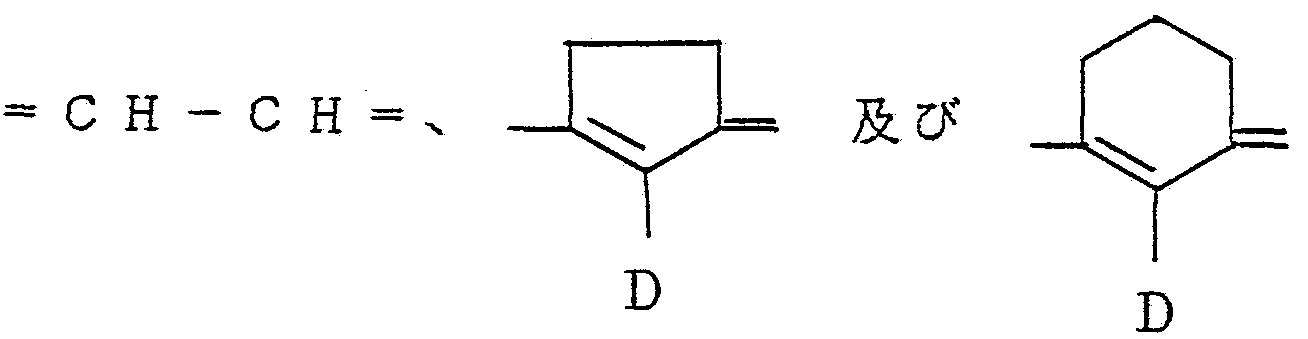
から選ばれ、 Dはハロゲン又は
ノ
一 を表わし、 β4と R5はそれぞれ置換基を有し又は有しないァ ヽ85
ルキル基又はフヱニル基を表わし、 ηιと Π2 はそれぞれ 0又ば自然
、
1 1
数であって、 i + n2 _ 2 であり、 X - はァニオ ンを表わす〕 であ ることを特徴とする電子写真用感光材料。
2. ボリ ビュル力ルバゾール又はその誘導体 1 gに対して增感色素 が 0.1 〜 1 0 0 の割合で配合されていることを特徴とする請求 の範囲第 1項記載の感光材料。
3 . ポリ ビュル力ルバゾール又はその誘導体 1 gに対して增感色素 が 0.25〜 5 m gの割合で配合されていることを特徴とする請求の範 囲第 1 項記載の感光材料。
4 . t と n2 がいずれ 1 であり、 A力く - C H - C H — C H =であ ることを特徴とする請求の範囲第 1 項記載の感光材料。
ノ CH3
5 . Yと Y ' がいずれも— であることを特徴とする請求の
\CH3
範囲第 1 項記載の感光材料。
6 . Zと Z ' がいずれも— N02 であることを特徴とする請求の範囲 第 5項記載の感光材料。
7 . Rtが- C3H1 7 であることを特徴とする請求の範囲第 6項記載の 感光材料。
8 . Xが C 04.— であるこ とを特徴とする特許請求の範囲第 6項記 載の感光材料。
9 . 基材と、 こ の基材の一面に設けられた導電層と、 こ の導電層上 に設けられた感光材料層とからなる電子写真用感光体において、 感 光材料層がポリ ビニルカルバゾール又はその誘導体と增感色素とを 主体とする感光材料からなり、 前記增感色素が一般式

〔式中 Yば S又は - , Y ' は S又は- C、 , ただし
\ R3 \β3 '
R2、 R3、 82 ' 及び! ?3 ' ばそれぞれアルキル基を表わし、 は と、 及び R2 ' は R3 ' とそれぞれ環を形成してもよ く、 Zと Z ' はそれぞ れハロゲン、 ニ ト ロ基、 シァノ基又ばアルキルスルホ二ル基を表わ し、 Rtと!? t ' はそれぞれ置換基を有し又は有しないアルキル基を表 わし、 Aは
- C H = C H - C H

D D
から選ばれ、 Dばハロゲン又は
- を表わし、 R4.と Rsはそれぞれ置換基を有し又は有しないァ \β5
ルキル基又はフ ヱニル基を表わし、 mと n2 はそれぞれ 0又は自然 数であって、 + η2 ^2であり、 X - はァニオ ンを表わす〕 であ ることを特徴とする電子写真用感光体
1 0 . ポリ ビュ ル力ルバゾー ル又はその誘導体 1 gに対して増感色 素が 0.1 〜 1 0 0 m gの割合で配合されていることを特徴とする請 求の範囲第 9項記載の感光体。
1 1 . ボ リ ビュル力ルバゾール又はその誘導体 1 gに対して增感色 素が 0,25〜 5 m gの割合で配合されていることを特徴とする請求の 範囲第 9項記載の感光体。
1 2 . n tと がいずれも 1 であり、 Aが— C H = C H C H -で あることを特徴とする請求の範囲第 9項記載の感光体。
-:、 ,' ·;-
ιηΛηηρ PCT/JP84/0025604825
1 3
CH3 _
1 3 Yと Y ' がいずれも— であることを特徴とする請求 ヽ CH3
の範囲第 9項記載の感光体。
1 4. Z と Z ' がいずれも— N02 であることを特徵とする請求の範 囲第 1 3項記載の感光体。
1 5. が - C8H17 であることを特徴とする請求の範囲第 1 4項記 載の感光体。
1 6 . Xが C ( - であることを特徴とする請求の範囲第 1 5項記 載の感光体。
Priority Applications (1)
| Application Number | Priority Date | Filing Date | Title |
|---|---|---|---|
| DE8484902060T DE3475440D1 (en) | 1983-05-24 | 1984-05-21 | Electrophotographic sensitized material |
Applications Claiming Priority (1)
| Application Number | Priority Date | Filing Date | Title |
|---|---|---|---|
| JP58090963A JPS59216146A (ja) | 1983-05-24 | 1983-05-24 | 電子写真用感光材料 |
Publications (1)
| Publication Number | Publication Date |
|---|---|
| WO1984004825A1 true WO1984004825A1 (fr) | 1984-12-06 |
Family
ID=14013147
Family Applications (1)
| Application Number | Title | Priority Date | Filing Date |
|---|---|---|---|
| PCT/JP1984/000256 Ceased WO1984004825A1 (fr) | 1983-05-24 | 1984-05-21 | Materiau electrophotographique sensibilise |
Country Status (5)
| Country | Link |
|---|---|
| US (1) | US4617247A (ja) |
| EP (1) | EP0147468B1 (ja) |
| JP (1) | JPS59216146A (ja) |
| DE (1) | DE3475440D1 (ja) |
| WO (1) | WO1984004825A1 (ja) |
Families Citing this family (134)
| Publication number | Priority date | Publication date | Assignee | Title |
|---|---|---|---|---|
| DE3513747A1 (de) * | 1985-04-17 | 1986-10-23 | Hoechst Ag, 6230 Frankfurt | Elektrophotographisches aufzeichnungsmaterial |
| JPS62223759A (ja) * | 1986-03-26 | 1987-10-01 | Sony Corp | 電子写真用感光体 |
| JPH0654394B2 (ja) * | 1986-11-14 | 1994-07-20 | 富士写真フイルム株式会社 | 光導電性組成物 |
| JPH0823707B2 (ja) * | 1987-04-22 | 1996-03-06 | 富士写真フイルム株式会社 | スキヤンニング露光工程を含む画像形成方法 |
| US4943638A (en) * | 1987-05-22 | 1990-07-24 | Minnesota Mining And Manufacturing Company | Dyes suitable for sensitization of photoconductive systems |
| GB8712151D0 (en) * | 1987-05-22 | 1987-06-24 | Minnesota Mining & Mfg | Dyes |
| JPH0199063A (ja) * | 1987-10-13 | 1989-04-17 | Tomoegawa Paper Co Ltd | 平版印刷用原版 |
| EP0342810A3 (en) * | 1988-05-20 | 1990-06-06 | Minnesota Mining And Manufacturing Company | Cyanine dyes and preparation thereof |
| DE60037951T2 (de) | 1999-05-21 | 2009-02-05 | Fujifilm Corp. | Fotoempfindliche Zusammensetzung und Flachdruckplatte, die diese Zusammensetzung verwendet |
| JP4469927B2 (ja) | 2000-05-23 | 2010-06-02 | Dic株式会社 | 感光性組成物およびこれを用いた平版印刷版原版、画像形成方法 |
| US6511790B2 (en) | 2000-08-25 | 2003-01-28 | Fuji Photo Film Co., Ltd. | Alkaline liquid developer for lithographic printing plate and method for preparing lithographic printing plate |
| EP2036721B1 (en) | 2000-11-30 | 2011-02-09 | FUJIFILM Corporation | Planographic printing plate precursor |
| CN100470365C (zh) | 2001-01-12 | 2009-03-18 | 富士胶片株式会社 | 正型成像材料 |
| JP2002341536A (ja) | 2001-05-21 | 2002-11-27 | Kodak Polychrome Graphics Japan Ltd | ネガ型感光性組成物およびネガ型感光性平版印刷版 |
| US20040067435A1 (en) | 2002-09-17 | 2004-04-08 | Fuji Photo Film Co., Ltd. | Image forming material |
| US7081330B2 (en) | 2002-09-20 | 2006-07-25 | Fuji Photo Film Co., Ltd. | Method of making lithographic printing plate |
| US7282321B2 (en) | 2003-03-26 | 2007-10-16 | Fujifilm Corporation | Lithographic printing method and presensitized plate |
| JP2005028774A (ja) | 2003-07-07 | 2005-02-03 | Fuji Photo Film Co Ltd | 平版印刷版用原版および平版印刷方法 |
| JP4291638B2 (ja) | 2003-07-29 | 2009-07-08 | 富士フイルム株式会社 | アルカリ可溶性ポリマー及びそれを用いた平版印刷版原版 |
| US20050153239A1 (en) | 2004-01-09 | 2005-07-14 | Fuji Photo Film Co., Ltd. | Lithographic printing plate precursor and lithographic printing method using the same |
| US20050208426A1 (en) | 2004-03-19 | 2005-09-22 | Fuji Photo Film Co., Ltd. | Method of making a planographic printing plate |
| ATE380117T1 (de) | 2004-04-09 | 2007-12-15 | Fujifilm Corp | Flachdruckplattenvorläufer und flachdruckverfahren. |
| EP1602982B1 (en) | 2004-05-31 | 2013-12-18 | FUJIFILM Corporation | Planographic printing method |
| JP2006021396A (ja) | 2004-07-07 | 2006-01-26 | Fuji Photo Film Co Ltd | 平版印刷版原版および平版印刷方法 |
| US7146909B2 (en) | 2004-07-20 | 2006-12-12 | Fuji Photo Film Co., Ltd. | Image forming material |
| US7425406B2 (en) | 2004-07-27 | 2008-09-16 | Fujifilm Corporation | Lithographic printing plate precursor and lithographic printing method |
| US20060032390A1 (en) | 2004-07-30 | 2006-02-16 | Fuji Photo Film Co., Ltd. | Lithographic printing plate precursor and lithographic printing method |
| JP2006058702A (ja) | 2004-08-20 | 2006-03-02 | Fuji Photo Film Co Ltd | 平版印刷版原版 |
| US7745090B2 (en) | 2004-08-24 | 2010-06-29 | Fujifilm Corporation | Production method of lithographic printing plate, lithographic printing plate precursor and lithographic printing method |
| JP2006062188A (ja) | 2004-08-26 | 2006-03-09 | Fuji Photo Film Co Ltd | 色画像形成材料及び平版印刷版原版 |
| JP4429116B2 (ja) | 2004-08-27 | 2010-03-10 | 富士フイルム株式会社 | 平版印刷版原版及び平版印刷版の製版方法 |
| JP2006068963A (ja) | 2004-08-31 | 2006-03-16 | Fuji Photo Film Co Ltd | 重合性組成物、それを用いた親水性膜、及び、平版印刷版原版 |
| JP5089866B2 (ja) | 2004-09-10 | 2012-12-05 | 富士フイルム株式会社 | 平版印刷方法 |
| JP4404734B2 (ja) | 2004-09-27 | 2010-01-27 | 富士フイルム株式会社 | 平版印刷版原版 |
| WO2006043408A1 (ja) | 2004-10-22 | 2006-04-27 | Amada Co., Ltd | 曲げ加工方法及びその装置 |
| US20060150846A1 (en) | 2004-12-13 | 2006-07-13 | Fuji Photo Film Co. Ltd | Lithographic printing method |
| JP2006181838A (ja) | 2004-12-27 | 2006-07-13 | Fuji Photo Film Co Ltd | 平版印刷版原版 |
| US7910286B2 (en) | 2005-01-26 | 2011-03-22 | Fujifilm Corporation | Lithographic printing plate precursor, lithographic printing method and packaged body of lithographic printing plate precursors |
| JP4474296B2 (ja) | 2005-02-09 | 2010-06-02 | 富士フイルム株式会社 | 平版印刷版原版 |
| EP1696268B1 (en) | 2005-02-28 | 2016-11-09 | FUJIFILM Corporation | Lithographic printing plate precursor |
| JP4538350B2 (ja) | 2005-03-18 | 2010-09-08 | 富士フイルム株式会社 | 感光性組成物および画像記録材料並びに画像記録方法 |
| JP4404792B2 (ja) | 2005-03-22 | 2010-01-27 | 富士フイルム株式会社 | 平版印刷版原版 |
| JP4574506B2 (ja) | 2005-03-23 | 2010-11-04 | 富士フイルム株式会社 | 平版印刷版原版、及びその製版方法 |
| JP4524235B2 (ja) | 2005-03-29 | 2010-08-11 | 富士フイルム株式会社 | 平版印刷版原版 |
| JP4815270B2 (ja) | 2005-08-18 | 2011-11-16 | 富士フイルム株式会社 | 平版印刷版の作製方法及び作製装置 |
| JP4759343B2 (ja) | 2005-08-19 | 2011-08-31 | 富士フイルム株式会社 | 平版印刷版原版および平版印刷方法 |
| JP4701042B2 (ja) | 2005-08-22 | 2011-06-15 | 富士フイルム株式会社 | 感光性平版印刷版 |
| CN101360965B (zh) | 2006-05-18 | 2010-12-22 | 富士胶片株式会社 | 被干燥物的干燥方法及装置 |
| JP4777226B2 (ja) | 2006-12-07 | 2011-09-21 | 富士フイルム株式会社 | 画像記録材料、及び新規化合物 |
| US8771924B2 (en) | 2006-12-26 | 2014-07-08 | Fujifilm Corporation | Polymerizable composition, lithographic printing plate precursor and lithographic printing method |
| JP2008163081A (ja) | 2006-12-27 | 2008-07-17 | Fujifilm Corp | レーザー分解性樹脂組成物およびそれを用いるパターン形成材料ならびにレーザー彫刻型フレキソ印刷版原版 |
| JP4881756B2 (ja) | 2007-02-06 | 2012-02-22 | 富士フイルム株式会社 | 感光性組成物、平版印刷版原版、平版印刷方法、及び新規シアニン色素 |
| JP5159123B2 (ja) | 2007-02-27 | 2013-03-06 | 富士フイルム株式会社 | 赤外線レーザ用感光性平版印刷版原版 |
| ATE471812T1 (de) | 2007-03-23 | 2010-07-15 | Fujifilm Corp | Negativ-lithografiedruckplattenvorläufer und lithografiedruckverfahren damit |
| JP4860525B2 (ja) | 2007-03-27 | 2012-01-25 | 富士フイルム株式会社 | 硬化性組成物及び平版印刷版原版 |
| EP1974914B1 (en) | 2007-03-29 | 2014-02-26 | FUJIFILM Corporation | Method of preparing lithographic printing plate |
| EP1975710B1 (en) | 2007-03-30 | 2013-10-23 | FUJIFILM Corporation | Plate-making method of lithographic printing plate precursor |
| EP1975706A3 (en) | 2007-03-30 | 2010-03-03 | FUJIFILM Corporation | Lithographic printing plate precursor |
| JP5046744B2 (ja) | 2007-05-18 | 2012-10-10 | 富士フイルム株式会社 | 平版印刷版原版、及びそれを用いた印刷方法 |
| EP2006738B1 (en) | 2007-06-21 | 2017-09-06 | Fujifilm Corporation | Lithographic printing plate precursor |
| EP2006091B1 (en) | 2007-06-22 | 2010-12-08 | FUJIFILM Corporation | Lithographic printing plate precursor and plate making method |
| ATE484386T1 (de) | 2007-07-02 | 2010-10-15 | Fujifilm Corp | Flachdruckplattenvorläufer und flachdruckverfahren damit |
| JP2009091555A (ja) | 2007-09-18 | 2009-04-30 | Fujifilm Corp | 硬化性組成物、画像形成材料及び平版印刷版原版 |
| JP2009069761A (ja) | 2007-09-18 | 2009-04-02 | Fujifilm Corp | 平版印刷版の製版方法 |
| KR20100061730A (ko) | 2007-09-19 | 2010-06-08 | 후지필름 가부시키가이샤 | 아세틸렌 화합물, 그 염, 그 축합물 및 그 조성물 |
| JP2009083106A (ja) | 2007-09-27 | 2009-04-23 | Fujifilm Corp | 平版印刷版用版面保護剤及び平版印刷版の製版方法 |
| JP4890403B2 (ja) | 2007-09-27 | 2012-03-07 | 富士フイルム株式会社 | 平版印刷版原版 |
| JP2009085984A (ja) | 2007-09-27 | 2009-04-23 | Fujifilm Corp | 平版印刷版原版 |
| JP2009086373A (ja) | 2007-09-28 | 2009-04-23 | Fujifilm Corp | ネガ型平版印刷版の現像方法 |
| JP4890408B2 (ja) | 2007-09-28 | 2012-03-07 | 富士フイルム株式会社 | 重合性組成物及びそれを用いた平版印刷版原版、アルカリ可溶性ポリウレタン樹脂、並びに、ジオール化合物の製造方法 |
| JP5055077B2 (ja) | 2007-09-28 | 2012-10-24 | 富士フイルム株式会社 | 画像形成方法および平版印刷版原版 |
| JP5002399B2 (ja) | 2007-09-28 | 2012-08-15 | 富士フイルム株式会社 | 平版印刷版原版の処理方法 |
| EP2042928B1 (en) | 2007-09-28 | 2010-07-28 | FUJIFILM Corporation | Negative-working photosensitive material and negative-working planographic printing plate precursor |
| JP4994175B2 (ja) | 2007-09-28 | 2012-08-08 | 富士フイルム株式会社 | 平版印刷版原版、及びそれに用いる共重合体の製造方法 |
| JP5244518B2 (ja) | 2007-09-28 | 2013-07-24 | 富士フイルム株式会社 | 平版印刷版原版及び平版印刷版の作製方法 |
| JP2009098688A (ja) | 2007-09-28 | 2009-05-07 | Fujifilm Corp | 平版印刷版原版、平版印刷版の作製方法および平版印刷方法 |
| JP4790682B2 (ja) | 2007-09-28 | 2011-10-12 | 富士フイルム株式会社 | 平版印刷版原版 |
| JP5322537B2 (ja) | 2007-10-29 | 2013-10-23 | 富士フイルム株式会社 | 平版印刷版原版 |
| EP2058123B1 (en) | 2007-11-08 | 2012-09-26 | FUJIFILM Corporation | Resin printing plate precursor for laser engraving, relief printing plate and method for production of relief printing plate |
| JPWO2009063824A1 (ja) | 2007-11-14 | 2011-03-31 | 富士フイルム株式会社 | 塗布膜の乾燥方法及び平版印刷版原版の製造方法 |
| JP2009139852A (ja) | 2007-12-10 | 2009-06-25 | Fujifilm Corp | 平版印刷版の作製方法及び平版印刷版原版 |
| JP2009186997A (ja) | 2008-01-11 | 2009-08-20 | Fujifilm Corp | 平版印刷版原版、平版印刷版の作製方法及び平版印刷版方法 |
| JP5155677B2 (ja) | 2008-01-22 | 2013-03-06 | 富士フイルム株式会社 | 平版印刷版原版、およびその製版方法 |
| JP5500831B2 (ja) | 2008-01-25 | 2014-05-21 | 富士フイルム株式会社 | レリーフ印刷版の作製方法及びレーザー彫刻用印刷版原版 |
| JP5241252B2 (ja) | 2008-01-29 | 2013-07-17 | 富士フイルム株式会社 | レーザー彫刻用樹脂組成物、レーザー彫刻用レリーフ印刷版原版、レリーフ印刷版及びレリーフ印刷版の製造方法 |
| JP2009184188A (ja) | 2008-02-05 | 2009-08-20 | Fujifilm Corp | 平版印刷版原版および印刷方法 |
| JP5150287B2 (ja) | 2008-02-06 | 2013-02-20 | 富士フイルム株式会社 | 平版印刷版の作製方法及び平版印刷版原版 |
| JP5137618B2 (ja) | 2008-02-28 | 2013-02-06 | 富士フイルム株式会社 | レーザー彫刻用樹脂組成物、レーザー彫刻用レリーフ印刷版原版、レリーフ印刷版及びレリーフ印刷版の製造方法 |
| EP2095970A1 (en) | 2008-02-29 | 2009-09-02 | Fujifilm Corporation | Resin composition for laser engraving, resin printing plate precursor for laser engraving, relief printing plate and method for production of relief printing plate |
| JP5175582B2 (ja) | 2008-03-10 | 2013-04-03 | 富士フイルム株式会社 | 平版印刷版の作製方法 |
| JP2009214428A (ja) | 2008-03-11 | 2009-09-24 | Fujifilm Corp | 平版印刷版原版および平版印刷方法 |
| JP2009236942A (ja) | 2008-03-25 | 2009-10-15 | Fujifilm Corp | 平版印刷版原版及びその製版方法 |
| JP5020871B2 (ja) | 2008-03-25 | 2012-09-05 | 富士フイルム株式会社 | 平版印刷版の製造方法 |
| JP5422134B2 (ja) | 2008-03-25 | 2014-02-19 | 富士フイルム株式会社 | 浸漬型平版印刷版用自動現像方法 |
| JP5422146B2 (ja) | 2008-03-25 | 2014-02-19 | 富士フイルム株式会社 | 平版印刷版作成用処理液および平版印刷版原版の処理方法 |
| US7923197B2 (en) | 2008-03-25 | 2011-04-12 | Fujifilm Corporation | Lithographic printing plate precursor |
| JP2009236355A (ja) | 2008-03-26 | 2009-10-15 | Fujifilm Corp | 乾燥方法及び装置 |
| EP2105298B1 (en) | 2008-03-28 | 2014-03-19 | FUJIFILM Corporation | Negative-working lithographic printing plate precursor and method of lithographic printing using same |
| JP5322575B2 (ja) | 2008-03-28 | 2013-10-23 | 富士フイルム株式会社 | レーザー彫刻用樹脂組成物、画像形成材料、レーザー彫刻用レリーフ印刷版原版、レリーフ印刷版、及びレリーフ印刷版の製造方法 |
| JP5305793B2 (ja) | 2008-03-31 | 2013-10-02 | 富士フイルム株式会社 | レリーフ印刷版及びレリーフ印刷版の製造方法 |
| JP5164640B2 (ja) | 2008-04-02 | 2013-03-21 | 富士フイルム株式会社 | 平版印刷版原版 |
| US20090260531A1 (en) | 2008-04-18 | 2009-10-22 | Fujifilm Corporation | Aluminum alloy plate for lithographic printing plate, lithographic printing plate support, presensitized plate, method of manufacturing aluminum alloy plate for lithographic printing plate and method of manufacturing lithographic printing plate support |
| JP5296434B2 (ja) | 2008-07-16 | 2013-09-25 | 富士フイルム株式会社 | 平版印刷版用原版 |
| JP5444933B2 (ja) | 2008-08-29 | 2014-03-19 | 富士フイルム株式会社 | ネガ型平版印刷版原版及びそれを用いる平版印刷方法 |
| JP5183380B2 (ja) | 2008-09-09 | 2013-04-17 | 富士フイルム株式会社 | 赤外線レーザ用感光性平版印刷版原版 |
| JP5398282B2 (ja) | 2008-09-17 | 2014-01-29 | 富士フイルム株式会社 | レーザー彫刻用樹脂組成物、レーザー彫刻用レリーフ印刷版原版、レリーフ印刷版の製造方法、及びレリーフ印刷版 |
| JP5449898B2 (ja) | 2008-09-22 | 2014-03-19 | 富士フイルム株式会社 | 平版印刷版原版、及びそれを用いた印刷方法 |
| JP5408942B2 (ja) | 2008-09-22 | 2014-02-05 | 富士フイルム株式会社 | 平版印刷版原版および製版方法 |
| JP2010102330A (ja) | 2008-09-24 | 2010-05-06 | Fujifilm Corp | 平版印刷版の作製方法 |
| JP5660268B2 (ja) | 2008-09-30 | 2015-01-28 | 富士フイルム株式会社 | 平版印刷版原版、平版印刷版の製版方法及び重合性モノマー |
| JP2010237435A (ja) | 2009-03-31 | 2010-10-21 | Fujifilm Corp | 平版印刷版原版 |
| CN102548769B (zh) | 2009-09-24 | 2015-08-12 | 富士胶片株式会社 | 平版印刷版原版 |
| US8828648B2 (en) | 2010-02-17 | 2014-09-09 | Fujifilm Corporation | Method for producing a planographic printing plate |
| JP5253433B2 (ja) | 2010-02-19 | 2013-07-31 | 富士フイルム株式会社 | 平版印刷版の作製方法 |
| EP2365389B1 (en) | 2010-03-08 | 2013-01-16 | Fujifilm Corporation | Positive-working lithographic printing plate precursor for infrared laser and process for making lithographic printing plate |
| EP2366546B1 (en) | 2010-03-18 | 2013-11-06 | FUJIFILM Corporation | Process for making lithographic printing plate and lithographic printing plate |
| CN102834779B (zh) | 2010-03-31 | 2015-07-08 | 富士胶片株式会社 | 用于处理平版印刷版原版的显影液,通过使用显影液制备平版印刷版的方法和印刷方法 |
| JP5662832B2 (ja) | 2010-08-31 | 2015-02-04 | 富士フイルム株式会社 | 画像形成材料、平版印刷版原版及び平版印刷版の作製方法 |
| JP5286350B2 (ja) | 2010-12-28 | 2013-09-11 | 富士フイルム株式会社 | 平版印刷版原版、その製版方法、及び、その平版印刷方法 |
| JP5241871B2 (ja) | 2011-03-11 | 2013-07-17 | 富士フイルム株式会社 | サーマルポジ型平版印刷版原版及び平版印刷版の作製方法 |
| JP5301015B2 (ja) | 2011-07-25 | 2013-09-25 | 富士フイルム株式会社 | 感光性平版印刷版原版及び平版印刷版の作製方法 |
| JP5255100B2 (ja) | 2011-07-29 | 2013-08-07 | 富士フイルム株式会社 | レーザー彫刻型フレキソ印刷版原版及びその製造方法、並びに、フレキソ印刷版及びその製版方法 |
| JP5438074B2 (ja) | 2011-08-12 | 2014-03-12 | 富士フイルム株式会社 | レーザー彫刻用フレキソ印刷版原版の製造方法 |
| JP5624003B2 (ja) | 2011-09-13 | 2014-11-12 | 富士フイルム株式会社 | 平版印刷版の製造方法及び平版印刷版 |
| WO2013039235A1 (ja) | 2011-09-15 | 2013-03-21 | 富士フイルム株式会社 | 製版処理廃液のリサイクル方法 |
| JP5690696B2 (ja) | 2011-09-28 | 2015-03-25 | 富士フイルム株式会社 | 平版印刷版の製版方法 |
| EP2762977B1 (en) | 2011-11-04 | 2017-09-27 | FUJIFILM Corporation | Method for recycling plate-making processing waste solution |
| JP5490168B2 (ja) | 2012-03-23 | 2014-05-14 | 富士フイルム株式会社 | 平版印刷版原版及び平版印刷版の作製方法 |
| CN104203588B (zh) | 2012-03-29 | 2017-03-08 | 富士胶片株式会社 | 平版印刷版原版、及其印刷方法 |
| JP5512730B2 (ja) | 2012-03-30 | 2014-06-04 | 富士フイルム株式会社 | 平版印刷版の作製方法 |
| JP5554362B2 (ja) | 2012-03-30 | 2014-07-23 | 富士フイルム株式会社 | 平版印刷版の製版方法 |
| JP5699112B2 (ja) | 2012-07-27 | 2015-04-08 | 富士フイルム株式会社 | 平版印刷版原版及びその製版方法 |
| CN105143983B (zh) | 2013-03-14 | 2019-10-22 | 富士胶片株式会社 | 制版处理废液的浓缩方法及再循环方法 |
| JP7114724B2 (ja) | 2018-09-20 | 2022-08-08 | 富士フイルム株式会社 | 硬化性組成物、硬化膜、赤外線透過フィルタ、積層体、固体撮像素子、センサ、及び、パターン形成方法 |
Citations (4)
| Publication number | Priority date | Publication date | Assignee | Title |
|---|---|---|---|---|
| US3619154A (en) * | 1968-07-30 | 1971-11-09 | Westvaco Corp | Infrared sensitization of photoconductive compositions employing cyanine dyes |
| JPS5629587A (en) * | 1979-08-21 | 1981-03-24 | Fuji Photo Film Co Ltd | 2,6-di-tert-butyl-4- 5- 2,6-di-tert-butyl-4h-thiopyran-4-ylidene penta-1,3-dienyl thiopyrylium salt and its preparation |
| JPS57157254A (en) * | 1981-02-23 | 1982-09-28 | Minnesota Mining & Mfg | Photosensitive layer and electronic photographic article |
| JPS5859453A (ja) * | 1981-10-06 | 1983-04-08 | Ricoh Co Ltd | 電子写真感光体 |
Family Cites Families (7)
| Publication number | Priority date | Publication date | Assignee | Title |
|---|---|---|---|---|
| FR1424425A (fr) * | 1963-06-10 | 1966-01-14 | Agfa Ag | émulsions photographiques d'halogénure d'argent sensibilisées optiquement |
| US3622316A (en) * | 1964-10-05 | 1971-11-23 | Polaroid Corp | Photoresponsive articles comprising multilayer spectral sensitization systems |
| DE2065695A1 (de) * | 1969-05-28 | 1975-10-30 | Fuji Photo Film Co Ltd | Photographische silberhalogenidemulsion |
| US3723116A (en) * | 1970-07-24 | 1973-03-27 | Canon Kk | Electrophotographic photosensitive materials |
| AU507694B2 (en) * | 1975-06-14 | 1980-02-21 | Hoechst Aktiengesellschaft | Electrophotographic reproduction |
| DE2942784C2 (de) * | 1978-10-27 | 1983-05-11 | Hitachi, Ltd., Tokyo | Elektrophotographisches Aufzeichnungsmaterial |
| DE3270544D1 (en) * | 1981-02-23 | 1986-05-22 | Minnesota Mining & Mfg | Sensitized organic electron donor compounds |
-
1983
- 1983-05-24 JP JP58090963A patent/JPS59216146A/ja active Granted
-
1984
- 1984-05-21 EP EP84902060A patent/EP0147468B1/en not_active Expired
- 1984-05-21 US US06/697,580 patent/US4617247A/en not_active Expired - Fee Related
- 1984-05-21 WO PCT/JP1984/000256 patent/WO1984004825A1/ja not_active Ceased
- 1984-05-21 DE DE8484902060T patent/DE3475440D1/de not_active Expired
Patent Citations (4)
| Publication number | Priority date | Publication date | Assignee | Title |
|---|---|---|---|---|
| US3619154A (en) * | 1968-07-30 | 1971-11-09 | Westvaco Corp | Infrared sensitization of photoconductive compositions employing cyanine dyes |
| JPS5629587A (en) * | 1979-08-21 | 1981-03-24 | Fuji Photo Film Co Ltd | 2,6-di-tert-butyl-4- 5- 2,6-di-tert-butyl-4h-thiopyran-4-ylidene penta-1,3-dienyl thiopyrylium salt and its preparation |
| JPS57157254A (en) * | 1981-02-23 | 1982-09-28 | Minnesota Mining & Mfg | Photosensitive layer and electronic photographic article |
| JPS5859453A (ja) * | 1981-10-06 | 1983-04-08 | Ricoh Co Ltd | 電子写真感光体 |
Non-Patent Citations (1)
| Title |
|---|
| See also references of EP0147468A4 * |
Also Published As
| Publication number | Publication date |
|---|---|
| JPS59216146A (ja) | 1984-12-06 |
| EP0147468A4 (en) | 1985-09-16 |
| JPH0447818B2 (ja) | 1992-08-05 |
| DE3475440D1 (en) | 1989-01-05 |
| US4617247A (en) | 1986-10-14 |
| EP0147468B1 (en) | 1988-11-30 |
| EP0147468A1 (en) | 1985-07-10 |
Similar Documents
| Publication | Publication Date | Title |
|---|---|---|
| WO1984004825A1 (fr) | Materiau electrophotographique sensibilise | |
| JPS6136232B2 (ja) | ||
| US3100703A (en) | Photographic process utilizing cyanine dye bases | |
| US4603098A (en) | Electrophotographic recording material | |
| CA1046265A (en) | Electrophotography photosensitive composition | |
| JPS6187647A (ja) | 混合スクアライン化合物の調整方法 | |
| JPS58178363A (ja) | 電子写真感光体 | |
| US3579331A (en) | Electrophotographic materials containing cyanine dye sensitizers | |
| JPH0331257B2 (ja) | ||
| US4562134A (en) | Electrophotographic material with cyanine sensitizer with betaine group | |
| JPH0231379B2 (ja) | ||
| US3518082A (en) | Method of electrophotographic imaging employing phenazine as the sensitizer for the photoconductive material | |
| JPS6177855A (ja) | 感光体 | |
| JPH02285357A (ja) | 電子写真感光体 | |
| JPS62223759A (ja) | 電子写真用感光体 | |
| US3595648A (en) | Poly-n-vinyl-3-nitro carbazole photoconductive material | |
| US3764320A (en) | Free radical dye transfer photographic process | |
| JPS60119565A (ja) | 電子写真感光体 | |
| JPH0789230B2 (ja) | 感光体 | |
| SU307594A1 (ru) | Электрофотографический материал | |
| JP3197128B2 (ja) | 電子写真感光体及び該電子写真感光体を備えた電子写真装置 | |
| JPS5857740B2 (ja) | ユウキコウハンドウタイデンシシヤシンザイリヨウ | |
| JPS59164558A (ja) | 電子写真感光材料 | |
| JPS60147742A (ja) | 電子写真感光体 | |
| JPS6177055A (ja) | 電子写真感光体 |
Legal Events
| Date | Code | Title | Description |
|---|---|---|---|
| AK | Designated states |
Designated state(s): US |
|
| AL | Designated countries for regional patents |
Designated state(s): DE FR GB NL |
|
| WWE | Wipo information: entry into national phase |
Ref document number: 1984902060 Country of ref document: EP |
|
| WWP | Wipo information: published in national office |
Ref document number: 1984902060 Country of ref document: EP |
|
| WWG | Wipo information: grant in national office |
Ref document number: 1984902060 Country of ref document: EP |