WO2012161458A2 - Appareil permettant d'inspecter une carte de circuits imprimés - Google Patents
Appareil permettant d'inspecter une carte de circuits imprimés Download PDFInfo
- Publication number
- WO2012161458A2 WO2012161458A2 PCT/KR2012/003832 KR2012003832W WO2012161458A2 WO 2012161458 A2 WO2012161458 A2 WO 2012161458A2 KR 2012003832 W KR2012003832 W KR 2012003832W WO 2012161458 A2 WO2012161458 A2 WO 2012161458A2
- Authority
- WO
- WIPO (PCT)
- Prior art keywords
- pcb substrate
- pcb
- inspection
- pair
- shuttles
- Prior art date
- Legal status (The legal status is an assumption and is not a legal conclusion. Google has not performed a legal analysis and makes no representation as to the accuracy of the status listed.)
- Ceased
Links
Images


Classifications
-
- G—PHYSICS
- G01—MEASURING; TESTING
- G01R—MEASURING ELECTRIC VARIABLES; MEASURING MAGNETIC VARIABLES
- G01R31/00—Arrangements for testing electric properties; Arrangements for locating electric faults; Arrangements for electrical testing characterised by what is being tested not provided for elsewhere
- G01R31/28—Testing of electronic circuits, e.g. by signal tracer
- G01R31/2801—Testing of printed circuits, backplanes, motherboards, hybrid circuits or carriers for multichip packages [MCP]
- G01R31/2806—Apparatus therefor, e.g. test stations, drivers, analysers, conveyors
- G01R31/2808—Holding, conveying or contacting devices, e.g. test adapters, edge connectors, extender boards
-
- H—ELECTRICITY
- H05—ELECTRIC TECHNIQUES NOT OTHERWISE PROVIDED FOR
- H05K—PRINTED CIRCUITS; CASINGS OR CONSTRUCTIONAL DETAILS OF ELECTRIC APPARATUS; MANUFACTURE OF ASSEMBLAGES OF ELECTRICAL COMPONENTS
- H05K13/00—Apparatus or processes specially adapted for manufacturing or adjusting assemblages of electric components
- H05K13/08—Monitoring manufacture of assemblages
- H05K13/081—Integration of optical monitoring devices in assembly lines; Processes using optical monitoring devices specially adapted for controlling devices or machines in assembly lines
- H05K13/0817—Monitoring of soldering processes
-
- H—ELECTRICITY
- H05—ELECTRIC TECHNIQUES NOT OTHERWISE PROVIDED FOR
- H05K—PRINTED CIRCUITS; CASINGS OR CONSTRUCTIONAL DETAILS OF ELECTRIC APPARATUS; MANUFACTURE OF ASSEMBLAGES OF ELECTRICAL COMPONENTS
- H05K13/00—Apparatus or processes specially adapted for manufacturing or adjusting assemblages of electric components
- H05K13/0061—Tools for holding the circuit boards during processing; handling transport of printed circuit boards
-
- H—ELECTRICITY
- H05—ELECTRIC TECHNIQUES NOT OTHERWISE PROVIDED FOR
- H05K—PRINTED CIRCUITS; CASINGS OR CONSTRUCTIONAL DETAILS OF ELECTRIC APPARATUS; MANUFACTURE OF ASSEMBLAGES OF ELECTRICAL COMPONENTS
- H05K13/00—Apparatus or processes specially adapted for manufacturing or adjusting assemblages of electric components
- H05K13/08—Monitoring manufacture of assemblages
- H05K13/081—Integration of optical monitoring devices in assembly lines; Processes using optical monitoring devices specially adapted for controlling devices or machines in assembly lines
- H05K13/0812—Integration of optical monitoring devices in assembly lines; Processes using optical monitoring devices specially adapted for controlling devices or machines in assembly lines the monitoring devices being integrated in the mounting machine, e.g. for monitoring components, leads, component placement
-
- H—ELECTRICITY
- H05—ELECTRIC TECHNIQUES NOT OTHERWISE PROVIDED FOR
- H05K—PRINTED CIRCUITS; CASINGS OR CONSTRUCTIONAL DETAILS OF ELECTRIC APPARATUS; MANUFACTURE OF ASSEMBLAGES OF ELECTRICAL COMPONENTS
- H05K13/00—Apparatus or processes specially adapted for manufacturing or adjusting assemblages of electric components
- H05K13/08—Monitoring manufacture of assemblages
- H05K13/081—Integration of optical monitoring devices in assembly lines; Processes using optical monitoring devices specially adapted for controlling devices or machines in assembly lines
- H05K13/0815—Controlling of component placement on the substrate during or after manufacturing
Definitions
- the present invention relates to a PCB substrate inspection apparatus, and more particularly, to a PCB substrate inspection apparatus capable of inspecting a PCB substrate stably and efficiently.
- SMT Surface Mounting Technology
- PCB substrates printed circuit boards
- SMD surface-mounting devices
- Surface mount lines consist of equipment such as surface mounters and vision inspection equipment.
- the surface mounter is a device for mounting a surface mount component on a PCB, and receives various surface mount components supplied in a tape, stick, and tray form from a feeder and places them on a mounting position on the PCB. .
- the vision inspection apparatus inspects the mounting state of the surface mount component before or after the soldering process of the surface mount component is completed and transfers the PCB to the next process according to the inspection result.
- a typical vision inspection apparatus includes a lighting unit to which light is irradiated using a lamp, and a camera unit which is installed on an upper portion of the lighting unit to photograph image information of various parts mounted on an inspection object.
- Conventional vision inspection method is to adjust the initial position in the positioning device when the inspection object is transported horizontally through the conveyor, and after the adjustment is completed, the lighting and the like irradiates the printed circuit board, and the camera and each surface-mounted component Take a picture of the lead.
- the image information is output to the monitor and calculated to inspect the quantity / defect of the surface-mounted component which is the inspection object, or to check whether the surface-mounted component is mounted or not.
- three-dimensional height is measured by irradiating light through a grating on a PCB substrate which is an inspection object and analyzing a shadow shape formed by the irradiated light on the surface of the inspection object.
- An object of the present invention is to provide a PCB substrate inspection apparatus that can efficiently and stably inspect a PCB substrate.
- Another object of the present invention is to provide a PCB substrate inspection apparatus which can improve inspection yield by enabling inspection of a PCB substrate quickly.
- Another object of the present invention is to provide a PCB substrate inspection apparatus capable of precisely aligning a PCB substrate.
- Another object of the present invention is to provide a PCB substrate inspection apparatus that can flexibly correspond to the width of a PCB substrate to be inspected.
- a PCB substrate inspection apparatus includes a pair of first and second inlet shuttles for transferring an incoming PCB to an inspection region, and a pair of first and second substrates for inspecting the PCB substrate.
- first and second discharge unit shuttles for receiving and discharging the finished PCB substrate from the first and second inspection unit conveyor parts at a position opposite to the sub shuttle.
- the first and second inspection unit conveyors are arranged in a fixed position, all may be configured to include a pair of conveyor belts, respectively.
- the pair of first and second inlet shuttles and the first and second outlet shuttles are configured to reciprocate in a direction perpendicular to the conveying direction of the PCB substrate by the pair of conveyor belts of the inlet shuttle. .
- first and second inlet shuttle may include a pair of inlet shuttle conveyor for transferring the PCB substrate in the direction of the inspection unit conveyor.
- the inspection unit conveyor each comprises a pair of PCB substrate transfer roller and the PCB substrate transfer belt.
- the inspection unit conveyor may be configured to include a PCB substrate support for elastically supporting the PCB substrate.
- the inspection unit conveyor may include a conveyor width adjusting member for adjusting a distance between the pair of PCB substrate transfer rollers and the PCB substrate transfer belt.
- the inspection unit conveyor includes a substrate stop member configured to move in the vertical direction to block the progress of the PCB substrate.
- the inspection unit conveyor may include a PCB sorting member for displacing the PCB substrate in a direction perpendicular to the direction conveyed by the pair of PCB substrate transfer belt.
- the inspection unit conveyor may include an inlet detection sensor for detecting an inlet of the PCB.
- the PCB substrate can be inspected efficiently and stably.
- the inspection yield can be improved by allowing the inspection of the PCB substrate to be performed quickly.
- the position of the PCB substrate can be precisely aligned.
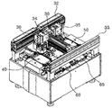
- FIG. 1 is a perspective view of a PCB substrate inspection apparatus according to the present invention.
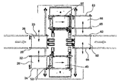
- FIG. 2 is a plan view of a PCB substrate inspection apparatus according to the present invention.
- FIG. 3 is a plan view of the inlet shuttle.
- FIG. 4 is a perspective view of the inspection unit conveyor.
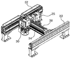
- 5 is a perspective view of the inspection unit.
- FIG. 1 is a perspective view of a PCB substrate inspection apparatus according to the present invention
- FIG. 2 is a plan view of a PCB substrate inspection apparatus according to the present invention
- FIG. 3 is a plan view of an inlet shuttle
- a PCB substrate inspection apparatus inspects a pair of first and second introduction shuttles 20 and 26 and a PCB substrate for transferring an inserted PCB substrate to an inspection region.
- the first and second discharge unit (60, 66) receiving the PCB substrate from the pair of first and second inspection unit (30, 35) and the first, second inlet shuttle (20, 26)
- a pair of first and second inspection unit conveyors 40 and 50 for delivery to the first and second inspection unit conveyors 40 and 50 at a position opposite to the first and second inlet shuttles 20 and 26; 50 and the first and second discharge unit shuttle (60, 66) for receiving and dispensing the finished PCB substrate.
- the inlet shuttle 20 and 26 are configured to receive a PCB substrate from a previous process, and include a pair of conveyor belts 22, 24, 23, and 25 configured to adjust an interval thereof, respectively. Placed in front.
- the pair of first and second pull-in shuttles 20 and 26 may be reciprocated in a direction perpendicular to the conveying direction of the PCB substrate by the pair of conveyor belts 22 and 24 of the pull-in shuttle 20. It is configured to be.
- the pair of inspection units 30 and 35 include a camera, a lens, and various lighting means to perform vision inspection on the PCB substrate, and a pair of lateral movement guides to move in the X and Y directions. It is arranged to be movable on the longitudinal movement guide members 34 and 36 movably disposed on the members 32 and 33.
- the pair of inspection unit conveyors 40 and 50 receive a PCB substrate from the inlet shuttles 20 and 26 in the inspection area 10 and arrange the PCB substrate below the inspection units 30 and 35. to be.
- the outlet shuttle 60, 66 includes a pair of conveyor belts 62, 64, 63, 65 that are configured to be adjustable in intervals, such as the inlet shuttle 20, respectively. It is arranged in the rear.
- the pair of discharge shuttles (60, 66) is also configured to be reciprocated in a direction perpendicular to the conveying direction of the PCB substrate by the pair of conveyor belts (62, 64, 63, 65), the overall In the configuration, it is substantially the same as the inlet shuttles 20 and 26.
- the inlet shuttle 20 and 26 each include a pair of PCB substrate transfer rollers 43 and a PCB substrate transfer belt 45.
- the PCB substrate can be received from the inlet and transferred to the inspection unit conveyors 40 and 50.
- the inlet shuttle 20, 26 includes a conveyor width adjusting member 47, 47-1 for adjusting the interval between the pair of belt for conveying the PCB substrate.
- One or more conveyor width detection sensors may be installed in the inlet shuttle 20 and 26 to adjust the conveyor width as described above.
- the inlet shuttle (20, 26) includes a substrate stop member (49) to allow the PCB substrate to stop at an appropriate position by the PCB substrate transfer belt 45.
- the substrate stop member 49 is configured to be movable in the vertical direction by, for example, a configuration such as an air cylinder, and when configured to stop the PCB substrate at a predetermined position, it is configured to descend to block the PCB substrate, When the inspection is completed, the PCB substrate to be transferred in the direction of the discharge shuttle 60 is configured to be raised so as not to disturb the transfer of the PCB substrate.
- At least one PCB detection sensor 53 may be installed at one side of the entrance shuttle 20 and 26 to detect the PCB substrate.
- the inlet shuttle 20, 26 is provided with a shuttle drive member 57 capable of reciprocating the inlet shuttle in the direction of the arrow of FIG.
- the shuttle driving member 57 is composed of, for example, a servo motor, a timing belt or a ball screw shaft, and the like, by rotating the timing belt 58 through a servo motor, or by rotating a ball screw shaft or the like through a servo motor.
- the inlet shuttle 20, 26 is configured to be moved in the direction of the arrow of Figure 2 on the guide rail (58-1).
- the inspection unit conveyor 40, 50 includes a PCB substrate support 46 is provided with a support pin 41 for elastically supporting the PCB substrate.
- the PCB when the PCB is mounted on the inspection unit conveyors 40 and 50, the PCB is elastically supported to prevent bending of the substrate.
- the inspection unit conveyor (40, 50) includes a conveyor width adjusting member (47-1) for adjusting the interval between a pair of PCB substrate transfer belt.
- One or more conveyor width detection sensors may be installed in the inspection unit conveyor 40 to adjust the conveyor width as described above.
- the inspection unit conveyor 40 also includes a substrate stop member 49-1 to allow the PCB substrate to be stopped at an appropriate position by the PCB substrate transfer belt 45.
- the substrate stop member 49-1 is also configured to be moved upward and downward by, for example, a configuration such as an air cylinder, so that when the PCB is to be stopped at a predetermined position, the substrate stop member 49 is lowered to block the PCB. And, when the inspection is completed, the PCB substrate to be transferred in the direction of the discharge shuttle 60 is configured so as not to interfere with the transfer of the PCB substrate.
- At least one PCB detection sensor may be installed at one side of the inspection unit conveyor 40 to detect the PCB.
- the PCB support plate 52 is also raised to continuously support the edge portion of the PCB substrate, thereby supporting the PCB substrate as a whole.
- the inspection unit conveyor 40 includes a PCB alignment member 51 for displacing the PCB substrate in a direction perpendicular to the direction transferred by the pair of PCB substrate transfer belts 45.
- the PCB substrate is pushed in the direction of the frame 42 opposite to the frame on which the PCB alignment member 51 is installed to align the position of the PCB substrate.
Landscapes
- Engineering & Computer Science (AREA)
- Microelectronics & Electronic Packaging (AREA)
- Manufacturing & Machinery (AREA)
- Operations Research (AREA)
- Computer Hardware Design (AREA)
- General Engineering & Computer Science (AREA)
- Physics & Mathematics (AREA)
- General Physics & Mathematics (AREA)
- Investigating Materials By The Use Of Optical Means Adapted For Particular Applications (AREA)
- Length Measuring Devices By Optical Means (AREA)
- Testing Of Short-Circuits, Discontinuities, Leakage, Or Incorrect Line Connections (AREA)
- Tests Of Electronic Circuits (AREA)
Abstract
Selon le mode de réalisation décrit dans l'invention, un appareil pour inspecter une carte de circuits imprimés (PCB) comprend: une paire de première et seconde navettes d'amenée conçues pour transférer une carte de circuits imprimés amenée vers une zone d'inspection; une paire de première et seconde unités d'inspection pour inspecter la carte de circuits imprimés; une paire de premier et second transporteurs d'unités d'inspection pour recevoir la carte de circuits imprimés provenant des première et seconde navette d'amenée puis pour transférer la carte de circuits imprimés dans les première et seconde navettes de sortie; et les première et seconde navettes de sortie pour recevoir puis faire sortir la carte de circuits imprimés ayant subit une inspection complète au moyen des premier et second transporteurs d'éléments d'inspection vers une position située en face des première et seconde navettes d'amenée. Selon la présente invention, la carte de circuits imprimés peut être inspectée de manière efficace et stable. En outre, la carte de circuits imprimés peut être rapidement inspectée afin d'améliorer un rendement d'inspection et de positionner précisément la carte de circuits imprimés.
Applications Claiming Priority (2)
| Application Number | Priority Date | Filing Date | Title |
|---|---|---|---|
| KR1020110047963A KR101178416B1 (ko) | 2011-05-20 | 2011-05-20 | 피시비 기판 검사장치 |
| KR10-2011-0047963 | 2011-05-20 |
Publications (2)
| Publication Number | Publication Date |
|---|---|
| WO2012161458A2 true WO2012161458A2 (fr) | 2012-11-29 |
| WO2012161458A3 WO2012161458A3 (fr) | 2013-01-17 |
Family
ID=46888085
Family Applications (1)
| Application Number | Title | Priority Date | Filing Date |
|---|---|---|---|
| PCT/KR2012/003832 Ceased WO2012161458A2 (fr) | 2011-05-20 | 2012-05-16 | Appareil permettant d'inspecter une carte de circuits imprimés |
Country Status (2)
| Country | Link |
|---|---|
| KR (1) | KR101178416B1 (fr) |
| WO (1) | WO2012161458A2 (fr) |
Cited By (1)
| Publication number | Priority date | Publication date | Assignee | Title |
|---|---|---|---|---|
| CN112485274A (zh) * | 2020-11-23 | 2021-03-12 | 苏州浪潮智能科技有限公司 | 一种电路板的运送装置及其控制方法 |
Families Citing this family (4)
| Publication number | Priority date | Publication date | Assignee | Title |
|---|---|---|---|---|
| KR101582896B1 (ko) * | 2014-12-19 | 2016-01-07 | (주)넥스티지 | 부품 부착 상태 검사 장치 |
| CN105691005B (zh) * | 2016-01-30 | 2017-08-22 | 江西中信华电子工业有限公司 | 一种自动打码设备 |
| DE102017102700A1 (de) * | 2017-02-10 | 2018-09-13 | Atg Luther & Maelzer Gmbh | Prüfvorrichtung und Verfahren zum Prüfen von Leiterplatten |
| KR101902966B1 (ko) | 2018-07-31 | 2018-11-22 | 오정기 | 기판 고정장치 |
Family Cites Families (4)
| Publication number | Priority date | Publication date | Assignee | Title |
|---|---|---|---|---|
| KR0139169Y1 (ko) * | 1996-09-24 | 1999-05-15 | 삼성전자주식회사 | Pcb 검사용 pcb 위치설정장치 |
| KR100270519B1 (ko) * | 1997-08-21 | 2001-01-15 | 구자홍 | 인쇄회로기판 검사 장치 |
| JP2000012999A (ja) | 1998-06-18 | 2000-01-14 | Nagoya Denki Kogyo Kk | 基板検査方法およびその装置 |
| JP4803195B2 (ja) * | 2008-03-14 | 2011-10-26 | パナソニック株式会社 | 基板検査装置及び基板検査方法 |
-
2011
- 2011-05-20 KR KR1020110047963A patent/KR101178416B1/ko active Active
-
2012
- 2012-05-16 WO PCT/KR2012/003832 patent/WO2012161458A2/fr not_active Ceased
Cited By (1)
| Publication number | Priority date | Publication date | Assignee | Title |
|---|---|---|---|---|
| CN112485274A (zh) * | 2020-11-23 | 2021-03-12 | 苏州浪潮智能科技有限公司 | 一种电路板的运送装置及其控制方法 |
Also Published As
| Publication number | Publication date |
|---|---|
| WO2012161458A3 (fr) | 2013-01-17 |
| KR101178416B1 (ko) | 2012-08-31 |
Similar Documents
| Publication | Publication Date | Title |
|---|---|---|
| WO2012157950A2 (fr) | Appareil d'inspection de support de carte de circuit imprimé | |
| WO2012121558A1 (fr) | Dispositif d'examen visuel ayant une clarté d'image améliorée | |
| KR101866942B1 (ko) | 배터리 셀 검사장치 | |
| WO2020027440A1 (fr) | Dispositif et procédé de vérification de défaut de surface, au moyen d'un capteur d'image | |
| WO2012121556A2 (fr) | Dispositif d'examen visuel utilisant un motif multigrille | |
| WO2012091344A2 (fr) | Appareil d'inspection visuelle | |
| WO2012161458A2 (fr) | Appareil permettant d'inspecter une carte de circuits imprimés | |
| WO2013048093A2 (fr) | Appareil et procédé d'inspection de composant sans contact | |
| WO2012053852A2 (fr) | Appareil d'inspection visuelle | |
| WO2016088990A1 (fr) | Module de plateau d'inspection à rayons x et appareil d'inspection à rayons x capable d'une inspection dans une direction inclinée utilisant ledit module | |
| WO2013009065A2 (fr) | Appareil pour contrôler la vision 3d d'un composant led et procédé de contrôle de vision | |
| WO2012157952A2 (fr) | Appareil d'inspection de support de carte de circuit imprimé | |
| WO2012134146A1 (fr) | Appareil pour inspecter la vision à l'aide d'une vision stéréo et d'un modèle de grille | |
| WO2013172568A1 (fr) | Appareil d'inspection de vision comprenant une partie d'éclairage apte à régler un angle de rayonnement de lumière | |
| CN116840157A (zh) | 一种用于pcb的多功能检测的装置 | |
| CN219810862U (zh) | 一种用于pcb电路板的双面aoi检测机构 | |
| KR102061221B1 (ko) | Pcb 제품 제조 시스템 | |
| CN107703649B (zh) | 用于同时检测多个待测料片的移载设备及其检测系统 | |
| KR101488160B1 (ko) | 피시비 기판의 냉각부를 포함하는 비전검사장치 | |
| WO2012134147A1 (fr) | Appareil d'inspection visuelle utilisant une grille de partition de la lumière visible et une grille de partition de la lumière invisible | |
| KR100715199B1 (ko) | 인쇄회로기판 자동 검사장비 | |
| KR101111065B1 (ko) | 기판검사장치 | |
| WO2012150782A1 (fr) | Dispositif d'essai visuel utilisant une plaque polarisante et un motif multi-réseau | |
| WO2012134145A1 (fr) | Appareil pour inspecter la vision à l'aide de modèles de grilles multiples ayant des couleurs différentes | |
| CN215142332U (zh) | 一种贴片引脚平正度影像检测装置 |
Legal Events
| Date | Code | Title | Description |
|---|---|---|---|
| 121 | Ep: the epo has been informed by wipo that ep was designated in this application |
Ref document number: 12789778 Country of ref document: EP Kind code of ref document: A2 |
|
| NENP | Non-entry into the national phase |
Ref country code: DE |
|
| 122 | Ep: pct application non-entry in european phase |
Ref document number: 12789778 Country of ref document: EP Kind code of ref document: A2 |