EP0096455B1 - Mehrschicht-Verbindungsstruktur für Halbleiteranordnung - Google Patents
Mehrschicht-Verbindungsstruktur für Halbleiteranordnung Download PDFInfo
- Publication number
- EP0096455B1 EP0096455B1 EP83301992A EP83301992A EP0096455B1 EP 0096455 B1 EP0096455 B1 EP 0096455B1 EP 83301992 A EP83301992 A EP 83301992A EP 83301992 A EP83301992 A EP 83301992A EP 0096455 B1 EP0096455 B1 EP 0096455B1
- Authority
- EP
- European Patent Office
- Prior art keywords
- interconnection
- layer
- insulating layer
- contact hole
- interconnection layer
- Prior art date
- Legal status (The legal status is an assumption and is not a legal conclusion. Google has not performed a legal analysis and makes no representation as to the accuracy of the status listed.)
- Expired
Links
Images
Classifications
-
- H—ELECTRICITY
- H10—SEMICONDUCTOR DEVICES; ELECTRIC SOLID-STATE DEVICES NOT OTHERWISE PROVIDED FOR
- H10W—GENERIC PACKAGES, INTERCONNECTIONS, CONNECTORS OR OTHER CONSTRUCTIONAL DETAILS OF DEVICES COVERED BY CLASS H10
- H10W20/00—Interconnections in chips, wafers or substrates
- H10W20/40—Interconnections external to wafers or substrates, e.g. back-end-of-line [BEOL] metallisations or vias connecting to gate electrodes
- H10W20/41—Interconnections external to wafers or substrates, e.g. back-end-of-line [BEOL] metallisations or vias connecting to gate electrodes characterised by their conductive parts
- H10W20/42—Vias, e.g. via plugs
Definitions
- This invention relates to an improvement on a multilayer interconnection structure for a semiconductor device and more particularly to an improvement on a contact hole pattern of said semiconductor device.
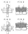
- Fig. 1 is a plan view of the conventional multilayer interconnection structure.
- Fig. 2 is a sectional view along line A-A of Fig. 1.
- a first interconnection layer 2 consisting of an impurity region is formed in the surface portion of a semiconductor substrate 1.
- a first insulating layer 3 is deposited on said surface.
- a contact hole 4 is bored in that part of the first insulating layer 3 which contacts the surface of the first interconnection layer 2.
- a second interconnection layer 5 prepared from aluminium is formed on the surface of the first insulating layer 3. This second interconnection layer 5 is connected to the first interconnection layer 2 by means of the contact hole 4.
- the contact hole 4 is relatively enlarged in that region where the first and second interconnection layers 2, 5 are superposed on each other, and extended along the second interconnection layer 5.
- a second insulating layer 6 is mounted on the first insulating layer 3 and second interconnection layer 5.
- a third interconnection layer 7 is laid on the second insulating layer 6. This third interconnection layer 7 crosses over the second interconnection layer 5 and passes over the contact hole 4.
- the conventional multilayer interconnection structure constructed as described above has the drawbacks that as seen from Fig. 2, a stepped portion of the second insulating layer 6 which is defined by the surface shape of the first insulating layer 3 above the contact hole 4 causes the third interconnection layer 7 to cover the second insulating layer 6 with less reliability. In other words, the third interconnection layer 7 is much thinner in the above-mentioned stepped portion of the second insulating layer 6.
- the conventional multilayer interconnection structure has the drawbacks that the third interconnection layer 7 tends to disconnect in the aforesaid stepped portion of the second insulating layer 6; wiring characteristics are deteriorated by, for example, increased wiring resistance; and electro-migration arises particularly in the thinned portion of the third interconnection layer 7, resulting in a decline in the reliability of a multilayer interconnection structure for a semiconductor device.
- US-A-4 260 436 discloses a multilayer interconnection structure for a semiconductor device having upper and lower interconnection layers deposited on a first insulating layer with a second insulating layer interposed between the upper and lower interconnection layers.
- the second insulating layer has a step portion in its upper surface above a contact hole formed in the first insulating layer.
- the upper interconnection layer crosses the lower interconnection layer above the contact hole.
- a multilayer interconnection structure for a semiconductor device comprising upper and lower interconnection layers (7, 5) deposited on the surface of a first insulating layer (3) deposited on a semiconductor substrate (1) with a second insulating layer (6) interposed between the upper and lower interconnection layers (7, 5), said second insulating layer (7) having a stepped portion in its upper surface above a contact hole (4) formed in the first insulating layer (3), said upper interconnection layer (7) crossing the lower interconnection layer (5) above the contact hole (4), characterized in that a plurality of contact holes (8a, 8b, 8c, 8d) are formed in the first insulating layer (3) and are linearly arranged in the direction in which the lower interconnection layer (5) extends and in that the upper interconnection layer (7) extends up over a portion of the first insulating layer (3) between adjacent contact holes.
- a multilayer interconnection structure embodying this invention has the advantages that the upper interconnection layer where it crosses the lower interconnection layer, passes over a portion of the lower interconnection layer between adjacent contact holes, thereby suppressing the disconnection of the interconnection layer and the increased resistance of wiring; and improvement is assured on the characteristics and reliability of a multilayer interconnection structure, thereby prominently increasing the application of said structure to the technical field of a semiconductor device.
- Fig. 3 of a multilayer interconnection structure according to a first embodiment of this invention.
- the parts of Fig. 3 the same as those of Fig. 1 are denoted by the same numerals, description thereof being omitted.
- the structure of Fig. 3 is different from that of Fig. 1 in that in the conventional multilayer interconnection structure, a single contact hole 4 is drilled in a state to cross the whole width of a third interconnection layer 7, while in the multilayer interconnection structure embodying this invention, a plurality of separate contact holes 8a, 8c, 8d are provided below the third interconnection layer 7. In other words, four small contact holes 8a, 8b, 8c, 8d are linearly drilled in the first insulating film 3 along the second interconnection layer 5.
- the third interconnection layer 7 In the multilayer interconnection structure arranged as described above, part of the transverse region of the third interconnection layer 7 in that section which crosses the second interconnection layer 5 does not overlap the contact holes 8a, 8b, 8c, 8d. Therefore, the above-mentioned portion of the third interconnection layer 7 passes a region free from any stepped portion.
- the section along line B-B of Fig. 3 indicates the same pattern as that of Fig. 2. Namely, the third interconnection layer 7 overlap the contact hole 8c and cross a stepped portion. In the section along line C-C of Fig. 3, however, the third interconnection layer 7 does not overlap any of the contact holes. As shown in Fig. 4, therefore, the third interconnection layer 7 crosses a step- free region.
- the embodiment of Fig. 3 offers the advantages that it is possible to suppress the disconnection of a third interconnection layer 7 in the stepped portion, and the cutting of wiring and increased wiring resistance caused by the reduced thickness of the thus interconnection layer 7, thereby assuring improvement in the characteristics and reliability of a multilayer interconnection structure.
- connection between adjacent interconnection layers through an intervening contact hole are governed not only by the area of the contact hole but also its peripheral length.
- a plurality of contact holes collectively occupy a smaller area than in the convention multilayer interconnection structure, but the total length of their peripheries is more enlarged. Therefore, the characteristics of connecting between adjacent interconnection layers deteriorate little.
- the interconnection layer and contact portion are prepared from aluminium, polysilicon, or refractory metal silicide.
- the number of contact holes need not be limited to four as previously described, but may be varied.
- the foregoing embodiments refer to the case where the substrate and the interconnection layer were connected together through a contact hole formed in the first insulating film.
- this invention is not limited to said embodiments, but is applicable to the case where any selected interconnection layers are connected together through a through hole formed in an insulating film interposed between said interconnection layers.
- the form "contact hole” is defined to include a through hole.
Landscapes
- Internal Circuitry In Semiconductor Integrated Circuit Devices (AREA)
Claims (1)
- Mehrschicht-Verbindungsstruktur für Halbleiteranordnung mit oberen und unteren Zwischenverbindungsschichten (7, 5), die auf die Oberfläche einer ersten Isolierschicht (3) aufgetragen sind, welche auf ein Halbleitersubstrat (1) aufgetragen ist, wobei sich eine zweite Isolierschicht (6) zwischen oberer und unterer Zwischenverbindungsschicht (7, 5) befindet, wobei die zweite Isolierschicht (6) einen abgestuften Teil in ihrer oberen Oberfläche über einem Kontaktloch (4) hat, das in der ersten Isolierschicht (3) ausgebildet ist, und wobei die obere Zwischenverbindungsschicht (7) die untere Zwischenverbindungsschicht (5) über dem Kontaktloch (4) kreuzt, dadurch gekennzeichnet, daß eine Vielzahl von Kontaktlöchern (8a, 8b, 8c, 8d) in der ersten Isolierschicht (3) ausgebildet und linear in der Richtung angeordnet sind, in der sich die untere Zwischenverbindungsschicht (5) erstreckt, und daß die obere Zwischenverbindungsschicht (7) sich über einen Teil der ersten Isolierschicht (3) zwischen benachbarten Kontaktlöchern erstreckt.
Applications Claiming Priority (2)
| Application Number | Priority Date | Filing Date | Title |
|---|---|---|---|
| JP96032/82 | 1982-06-04 | ||
| JP57096032A JPS58213450A (ja) | 1982-06-04 | 1982-06-04 | 半導体装置の多層配線構造 |
Publications (4)
| Publication Number | Publication Date |
|---|---|
| EP0096455A2 EP0096455A2 (de) | 1983-12-21 |
| EP0096455A3 EP0096455A3 (en) | 1985-08-07 |
| EP0096455B1 true EP0096455B1 (de) | 1988-07-06 |
| EP0096455B2 EP0096455B2 (de) | 1992-03-18 |
Family
ID=14154079
Family Applications (1)
| Application Number | Title | Priority Date | Filing Date |
|---|---|---|---|
| EP83301992A Expired - Lifetime EP0096455B2 (de) | 1982-06-04 | 1983-04-08 | Mehrschicht-Verbindungsstruktur für Halbleiteranordnung |
Country Status (4)
| Country | Link |
|---|---|
| US (1) | US4587549A (de) |
| EP (1) | EP0096455B2 (de) |
| JP (1) | JPS58213450A (de) |
| DE (1) | DE3377312D1 (de) |
Families Citing this family (13)
| Publication number | Priority date | Publication date | Assignee | Title |
|---|---|---|---|---|
| JPS60206164A (ja) * | 1984-03-30 | 1985-10-17 | Toshiba Corp | 半導体メモリ装置 |
| JPS60211866A (ja) * | 1984-04-05 | 1985-10-24 | Mitsubishi Electric Corp | 半導体集積回路 |
| JPS6276640A (ja) * | 1985-09-30 | 1987-04-08 | Toshiba Corp | 半導体集積回路装置 |
| JPS62274659A (ja) * | 1986-05-22 | 1987-11-28 | Mitsubishi Electric Corp | 半導体装置 |
| DE3641299A1 (de) * | 1986-12-03 | 1988-06-16 | Philips Patentverwaltung | Integrierte halbleiter-schaltung mit mehrlagenverdrahtung |
| DE3902693C2 (de) * | 1988-01-30 | 1995-11-30 | Toshiba Kawasaki Kk | Mehrebenenverdrahtung für eine integrierte Halbleiterschaltungsanordnung und Verfahren zur Herstellung von Mehrebenenverdrahtungen für integrierte Halbleiterschaltungsanordnungen |
| US4975544A (en) * | 1988-03-18 | 1990-12-04 | Fujitsu Limited | Connecting structure for connecting conductors in an electronic apparatus |
| JP3238395B2 (ja) * | 1990-09-28 | 2001-12-10 | 株式会社東芝 | 半導体集積回路 |
| US5466961A (en) * | 1991-04-23 | 1995-11-14 | Canon Kabushiki Kaisha | Semiconductor device and method of manufacturing the same |
| US5185652A (en) * | 1991-05-28 | 1993-02-09 | Ncr Corporation | Electrical connection between buses on a semiconductor integrated circuit |
| GB2276491A (en) * | 1993-03-26 | 1994-09-28 | Lucas Ind Plc | Multilayered connections for intergrated circuits |
| DE4328474C2 (de) * | 1993-08-24 | 1996-09-12 | Gold Star Electronics | Mehrschichtverbindungsstruktur für eine Halbleitereinrichtung |
| US6251773B1 (en) | 1999-12-28 | 2001-06-26 | International Business Machines Corporation | Method of designing and structure for visual and electrical test of semiconductor devices |
Family Cites Families (17)
| Publication number | Priority date | Publication date | Assignee | Title |
|---|---|---|---|---|
| US3436611A (en) * | 1965-01-25 | 1969-04-01 | Texas Instruments Inc | Insulation structure for crossover leads in integrated circuitry |
| US3436616A (en) * | 1967-02-07 | 1969-04-01 | Motorola Inc | Ohmic contact consisting of a bilayer of gold and molybdenum over an alloyed region of aluminum-silicon |
| JPS4828185A (de) * | 1971-08-18 | 1973-04-13 | ||
| JPS50141975A (de) * | 1974-05-01 | 1975-11-15 | ||
| DE2460150C2 (de) * | 1974-12-19 | 1984-07-12 | Ibm Deutschland Gmbh, 7000 Stuttgart | Monolitisch integrierbare Speicheranordnung |
| JPS584819B2 (ja) * | 1975-08-28 | 1983-01-27 | 株式会社東芝 | ハンドウタイソウチ |
| JPS5947474B2 (ja) * | 1975-10-31 | 1984-11-19 | 株式会社東芝 | ハンドウタイソウチ |
| US4185294A (en) * | 1975-12-10 | 1980-01-22 | Tokyo Shibaura Electric Co., Ltd. | Semiconductor device and a method for manufacturing the same |
| JPS5279679A (en) * | 1975-12-26 | 1977-07-04 | Toshiba Corp | Semiconductor memory device |
| JPS5839380B2 (ja) * | 1977-02-28 | 1983-08-30 | 沖電気工業株式会社 | 半導体集積回路装置 |
| JPS55132055A (en) * | 1979-03-30 | 1980-10-14 | Nec Corp | Mos integrated circuit |
| JPS55134962A (en) * | 1979-04-09 | 1980-10-21 | Toshiba Corp | Semiconductor device |
| DE3177173D1 (de) * | 1980-01-25 | 1990-05-23 | Toshiba Kawasaki Kk | Halbleiterspeichervorrichtung. |
| US4260436A (en) * | 1980-02-19 | 1981-04-07 | Harris Corporation | Fabrication of moat resistor ram cell utilizing polycrystalline deposition and etching |
| GB2073951B (en) * | 1980-04-11 | 1984-10-03 | Hitachi Ltd | Multilayer interconnections for an integrated circuit |
| JPS5726454A (en) * | 1980-07-24 | 1982-02-12 | Nec Corp | Integrated circuit device |
| JPS5773940A (en) * | 1980-10-28 | 1982-05-08 | Toshiba Corp | Levelling method of insulation layer |
-
1982
- 1982-06-04 JP JP57096032A patent/JPS58213450A/ja active Granted
-
1983
- 1983-04-07 US US06/482,783 patent/US4587549A/en not_active Expired - Lifetime
- 1983-04-08 DE DE8383301992T patent/DE3377312D1/de not_active Expired
- 1983-04-08 EP EP83301992A patent/EP0096455B2/de not_active Expired - Lifetime
Also Published As
| Publication number | Publication date |
|---|---|
| JPS58213450A (ja) | 1983-12-12 |
| EP0096455A3 (en) | 1985-08-07 |
| DE3377312D1 (en) | 1988-08-11 |
| EP0096455A2 (de) | 1983-12-21 |
| EP0096455B2 (de) | 1992-03-18 |
| US4587549A (en) | 1986-05-06 |
| JPS6343895B2 (de) | 1988-09-01 |
Similar Documents
| Publication | Publication Date | Title |
|---|---|---|
| EP0096455B2 (de) | Mehrschicht-Verbindungsstruktur für Halbleiteranordnung | |
| US7205636B2 (en) | Semiconductor device with a multilevel interconnection connected to a guard ring | |
| US7087496B2 (en) | Seal ring for integrated circuits | |
| US5216280A (en) | Semiconductor integrated circuit device having pads at periphery of semiconductor chip | |
| US20060244156A1 (en) | Bond pad structures and semiconductor devices using the same | |
| KR20000037768A (ko) | 다마신 금속배선 및 그 형성방법 | |
| US5561327A (en) | Multilayer interconnection structure for a semiconductor device | |
| EP0431490B1 (de) | Integrierte Halbleiterschaltungsvorrichtung mit Kontaktierungsflächen am Rande des Halbleiterchips | |
| JP3109478B2 (ja) | 半導体装置 | |
| US6236114B1 (en) | Bonding pad structure | |
| JPH04167449A (ja) | 半導体装置 | |
| JPH031538A (ja) | 半導体装置 | |
| US20030222274A1 (en) | Semiconductor integrated circuit device | |
| US6414393B2 (en) | Semiconductor device | |
| JP2693750B2 (ja) | 半導体装置 | |
| JP2508831B2 (ja) | 半導体装置 | |
| KR100532387B1 (ko) | 반도체 칩의 패드 | |
| JP2000164696A (ja) | 多層配線構造 | |
| JP2004327551A (ja) | 半導体集積回路装置 | |
| JP2000232103A (ja) | 半導体装置 | |
| JPS63253644A (ja) | 半導体装置 | |
| JPH03116852A (ja) | 半導体装置 | |
| JPH04188753A (ja) | 多層配線半導体装置 | |
| JPS6173347A (ja) | 半導体装置 | |
| JPS63226944A (ja) | 半導体装置 |
Legal Events
| Date | Code | Title | Description |
|---|---|---|---|
| PUAI | Public reference made under article 153(3) epc to a published international application that has entered the european phase |
Free format text: ORIGINAL CODE: 0009012 |
|
| 17P | Request for examination filed |
Effective date: 19830415 |
|
| AK | Designated contracting states |
Designated state(s): DE FR GB IT NL |
|
| RAP1 | Party data changed (applicant data changed or rights of an application transferred) |
Owner name: KABUSHIKI KAISHA TOSHIBA |
|
| PUAL | Search report despatched |
Free format text: ORIGINAL CODE: 0009013 |
|
| AK | Designated contracting states |
Designated state(s): DE FR GB IT NL |
|
| 17Q | First examination report despatched |
Effective date: 19861024 |
|
| GRAA | (expected) grant |
Free format text: ORIGINAL CODE: 0009210 |
|
| AK | Designated contracting states |
Kind code of ref document: B1 Designated state(s): DE IT NL |
|
| ITF | It: translation for a ep patent filed | ||
| REF | Corresponds to: |
Ref document number: 3377312 Country of ref document: DE Date of ref document: 19880811 |
|
| PLBI | Opposition filed |
Free format text: ORIGINAL CODE: 0009260 |
|
| 26 | Opposition filed |
Opponent name: DEUTSCHE ITT INDUSTRIES GMBH, FREIBURG Effective date: 19890406 Opponent name: TELEFUNKEN ELECTRONIC GMBH Effective date: 19890405 |
|
| NLR1 | Nl: opposition has been filed with the epo |
Opponent name: DEUTSCHE ITT INDUSTRIES GMBH Opponent name: TELEFUNKEN ELECTRONIC GMBH |
|
| ITTA | It: last paid annual fee | ||
| PUAH | Patent maintained in amended form |
Free format text: ORIGINAL CODE: 0009272 |
|
| STAA | Information on the status of an ep patent application or granted ep patent |
Free format text: STATUS: PATENT MAINTAINED AS AMENDED |
|
| 27A | Patent maintained in amended form |
Effective date: 19920318 |
|
| AK | Designated contracting states |
Kind code of ref document: B2 Designated state(s): DE IT NL |
|
| NLR2 | Nl: decision of opposition | ||
| NLR3 | Nl: receipt of modified translations in the netherlands language after an opposition procedure | ||
| PGFP | Annual fee paid to national office [announced via postgrant information from national office to epo] |
Ref country code: DE Payment date: 20020417 Year of fee payment: 20 |
|
| PGFP | Annual fee paid to national office [announced via postgrant information from national office to epo] |
Ref country code: NL Payment date: 20020426 Year of fee payment: 20 |
|
| PG25 | Lapsed in a contracting state [announced via postgrant information from national office to epo] |
Ref country code: NL Free format text: LAPSE BECAUSE OF EXPIRATION OF PROTECTION Effective date: 20030408 |