EP0097889A2 - Treiberschaltung mit Mitteln zum Verringern selbstinduzierten Schaltrauschens - Google Patents
Treiberschaltung mit Mitteln zum Verringern selbstinduzierten Schaltrauschens Download PDFInfo
- Publication number
- EP0097889A2 EP0097889A2 EP83105926A EP83105926A EP0097889A2 EP 0097889 A2 EP0097889 A2 EP 0097889A2 EP 83105926 A EP83105926 A EP 83105926A EP 83105926 A EP83105926 A EP 83105926A EP 0097889 A2 EP0097889 A2 EP 0097889A2
- Authority
- EP
- European Patent Office
- Prior art keywords
- current
- chip
- driver circuit
- driver
- noise
- Prior art date
- Legal status (The legal status is an assumption and is not a legal conclusion. Google has not performed a legal analysis and makes no representation as to the accuracy of the status listed.)
- Granted
Links
Images
Classifications
-
- H—ELECTRICITY
- H03—ELECTRONIC CIRCUITRY
- H03K—PULSE TECHNIQUE
- H03K17/00—Electronic switching or gating, i.e. not by contact-making and –breaking
- H03K17/16—Modifications for eliminating interference voltages or currents
Definitions
- This invention relates to a monolithic integrated driver circuit with means for reducing self-induced switching noise (Delta-I noise) caused by the inherent package inductance in semiconductor chips.
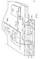
- Fig. 1 shows two communicating chips, "Chip 1" and "Chip 2" within a MCM.
- Fig. 1 shows Chip 1 utilized as a driver indicated by the Transistor Tl while Chip 2 is used as a receiver indicated by a terminating resistor, RT.
- a module section "module” interconnects the two chips and contains a signal line and two reference planes disposed on either side of the signal line. Two power vias disposed underneath each of the chip sites are coupled through large decoupling capacitances C10 and Cll on the board.
- Fig. 1 shows a fraction of the current passing back toward the sending chip while the remainder goes to the board through the decoupling capacitors Cll and back up to the Chip 2 VC reference plane. This is shown by the dotted line arrow in the righthand portion of Fig. 1.
- a negative Delta-I noise component is introduced at the Chip 1 VC and a positive Delta-I noise component is introduced at the Chip 2 GND.
- these noise components may propagate onto quiet lines potentially resulting in false switching of quiet receivers and may also disturb on chip logic gates.
- an important consideration in reducing system susceptibility to noise is the ability to reduce the magnitude of the effective package inductance. Such a reduction produces a corresponding reduction in the magnitude of the noise component.
- one technique for reducing effective package inductance is to have the high frequency noise current circulate near the top of the module as opposed to traveling down to the board. Such a path would bypass most of the module and the board inductance.
- a potential technique for accomplishing this goal would be to introduce top surface module decoupling capacitors.
- this solution is currently not feasible for use with practiced MCM techniques. Available decoupling capacitors are not compatible with existing MCM technology because excessive topside area would have to be set aside for their inclusion. This would reduce the number of chips and circuits that could be placed on the MCM significantly detracting from its overall performance and economic advantages.
- additional power planes would have to be added at the top of the MCM to provide a low inductance path between the capacitors and the chips making the module even more complex and more expensive to produce.
- Noise suppression circuits are shown generally in U.S. Patents 3 816 762 and 3 898 482. Also, integrated circuit clamping circuits are shown in U.S. Patents 3 188 499; 3 654 530; 3 816 762; 3 898 482; 4 027 177; 4 085 432; 4 178 521; 4 216 393; 4 239 989 and 4 131 928.
- Those prior art patents do not deal specifically with the concept of reducing effective package inductance by rerouting the high frequency noise currents for circulation near the top of the module. Rather, they deal with circuits to suppress noise rather than attempting to eliminate the noise components per se.
- the invention as claimed is intended to remedy these drawbacks. It solves the problem of how to reduce the self-induced switching noise (Delta-I noise) caused by the inherent package inductance in semiconductor chips by creating an on-chip impedance characteristic that interconnects the power supplies and off chip driver transistor allowing module currents to complete their loops on-chip, so that a low impedance path for noise current is defined that will flow near the top of a module and bypass a majority of package inductance.
- Delta-I noise self-induced switching noise
- the advantages of this invention are accomplished by first defining an on-chip impedance characteristic connecting the power supplies and off-chip driver transistor that allow the module currents to complete their loops on-chip.
- driver circuit means a resistor and the characteristics of a P-N diode junction.
- the resistor and one or more diodes are connected in series between the positive and negative supply so as to forward bias the diode(s).
- the driver transistor collector is connected at the resistor-diode connection.
- the forward biased diode junction builds up an anode-cathode capacitance as a function of the forward bias current. This capacitance permits the transient currents to travel between the VC and ground power supplies and the driver transistor collector.
- This circuit also acts as a shunt current regulator to reduce the low frequency noise produced by the differences in VC current demand by the driver transistor from the high and low input signals.
- this circuit is placed between the VC and the GND power chip leads and connected to driver collector then when noise is generated by switching of the drivers there is a low impedance path for the noise current to flow near the top of the module. This effectively bypasses most of the package inductance causing a significant reduction in Delta-I noise. Moreover, the noise current flow now is directed through parallel via paths VC and GND to each chip thereby further reducing the effective inductance.
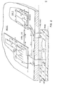
- the bypassed emitter follower driver circuit includes a driver transistor Tl, the collector of which is connected, at node A, to the anode of diode TSl and current limiting resistor RC and the emitter of which is connected, at node C, to an off-chip signal line SL1.
- the base of driver transistor Tl is connected to an input signal.
- the input signal source is the output of another digital circuit or special circuit designed to provide proper input signals for transistor Tl.
- Diodes TS1 and TS2 are connected in series, such that the cathode of diode TSl is connected to the anode of diode TS2.
- the cathode of diode TS2 is connected to module ground.
- Diodes TS1 and TS2 are preferably the base-collector junction of a transistor, which provides appreciable capacitance as a function of forward current flow.
- Current limiting resistor is connected between chip VC and a node A. It will limit the amount of current to diodes TS1 and TS2.
- Inductor Ll connects the chip VC to the board VC, while inductor L2 connects the chip ground to the board ground. These two inductors are the effective wiring inductance to the board supply of VC and ground. Resistor RT is connected between node B and chip ground. It is the terminating impedance for the signal line SL1 which is connected between node C, the driver transistor Tl emitter, and node B. Resistor RT is located on another chip.
- the input signal at the base of driver transistor Tl is low, so that the collector current of transistor Tl is low supplying only the small amount of current for terminating resistor RT.
- Diodes TS1 and TS2 are forward biased, clamping the voltage at node A at two forward diode drops above chip ground.
- the current through the diodes TSl and TS2 is determined by resistor RC, the diode characteristics of diodes TS1 and TS2 and the voltage across the series connected resistor RC and diodes TS1 and TS2 and the small amount of current required by driver transistor Tl for terminating resistor RT. It should be noted that the current through resistor RC is the sum of transistor Tl collector current and diodes TS1 and TS2 biasing current.
- a diode has two types of capacitance associated therewith.
- the first capacitance is generally referred to as depletion capacitance and is due to the charge depletion at the PN diode junction.
- the depletion capacitance is dominant under reverse bias conditions.
- the second capacitance is referred to as the diffusion or charge storage capacitance which arises from the lagging behind of voltage as current changes, due to charge storage effects.
- the diffusion or charge storage capacitance is dominant under forward bias conditions, and is an exponential function of the current through the junction.
- Diodes TS1 and TS2 are forward biased, the diffusion or charge storage capacitance dominates.
- Diodes TS1 and TS2 are preferably each a base-collector junction but could also be a base-emitter junction, or a base-collector junction in series with a base-emitter junction.
- diodes TS1 and TS2 provide two important functions. First, the diode current-voltage characteristics reduce the current through the two diodes as node A voltage drops, switching the current to transistor Tl. The current previously going through diodes TS1 and TS2 now goes through transistor Tl. Diodes TS1 and TS2 are regulating the current through RC. As the voltage drops at node A the ability of diodes TS1 and TS2 to regulate the current through RC diminishes.
- This shunt regulator effect minimizes the changes in IR drop for the VC supply wiring and ground supply wiring. Since the off chip drivers (such as transistor Tl) change state infrequently, as compared to the speed at which the off chip driver goes from a high level to a low level, the shunt regulator effect will reduce the low frequency VC supply and ground supply wiring IR drop.
- the second function of transistor junctions TS1 and TS2, as node A voltage drops, is to provide bypass capacitance.
- a forward biased diode forms an anode-cathode capacitance as a function of its forward current. This capacitance becomes large as the current is increased. This phenomena is used in the circuit to provide a bypass to ground capacitance for node A.
- the diode junction capacitance provides and AC current path from ground, reducing the transient current through resistor RC. This provides AC return path for the transient current in the chip ground supply.
- transistor Tl When the signal "in” is at an Up level, transistor Tl is providing DC current to the off chip circuit.
- the diode junctions of TS1 and TS2 are off or at a very low current level, providing no function in the circuit. This DC condition causes no transient conditions to the chip power supply.
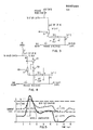
- Fig. 5 compares the current through inductor Ll of Fig. 3, the uncompensated driver circuit, to the current through inductor Ll of Fig. 4, the compensated driver circuit. From time 0 to time 2 the inputs of the two circuits are steady state. The current is higher for the compensated circuit since the diodes TS1 and TS2 are conducting current. The diodes are forward biased and have large anode-cathode capacitance characteristics. At time 2 the input signal to both circuits (Figs. 3 and 4) goes high. Although not described previously, signal line SLI in both Figs. 3 and 4 has capacitive characteristics which increases the transient VC supply and ground supply currents.
- the uncompensated circuit provides a 4.4 mA ( ⁇ I) change in current from the VC board supply, which produces a voltage change at the chip VC supply equal to Ll ⁇ I VC / ⁇ T.
- the compensated circuit during this transition is capacitively coupling the transient from the ground supply to the driver transistor collector using the capacitance of diodes TSl and TS2 in Fig. 4.
- the compensated circuit provides a 2.3 mA ( ⁇ I) change in current from the VC board supply, which produces a voltage change at the chip VC supply equal to Ll ⁇ I VCcomp /AT. Since the compensated circuit has a smaller ⁇ I it will have a smaller voltage change at the chip VC supply.
- the input signal goes to a low level.
- the current required by both circuits decrease.
- the current for the uncompensated circuit goes to OmA at time 12 due to the capacitive characteristics of signal line SL1.
- Resistor RT in Fig. 3 must discharge the capacitance of signal line SL1.
- the capacitance is discharged and driver transistor Tl turns on.
- the ⁇ I for this negative going transition at time 12 is 2.3 mA.
- the compensated circuit is also driving the signal line SL1 with its capacitive characteristics.
- diodes TS1 and TS2 in Fig. 4 become forward biased, conducting the transient current to ground supply as described previously. This results in a smaller AI of 1 mA.
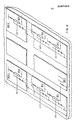
- Fig. 6 shows two typical chips mounted on a module. Both chip 1 and chip 2 have a number of compensated drivers on each chip.
- the compensated driver is the type shown in Fig. 4.
- the drivers on each chip can be described as active, an input transition applied to the input, or described as inactive, the input is at a DC level.
- the inactive driver can have one of two inputs. Referring to Fig. 4, a high level input to driver transistor Tl pulls node A low as described previously. Diodes TS1 and TS2 although forward biased, conduct very little current and the anode to cathode capacitance is relatively small. In this state, the compensating circuit has little impact on decoupling the VC supply to the ground supply other than as previously described for an active driver. When the input to driver transistor Tl is low, diodes TSl and TS2 are forward biased and the anode to cathode capacitance is high.
- resistor RC and diodes TS1 and TS2 provide a low impedance path for transients between the VC supply and ground supply.
- resistor RC and diodes TS1 and TS2 provide a low impedance path for transients between the VC supply and ground supply.
Landscapes
- Semiconductor Integrated Circuits (AREA)
- Logic Circuits (AREA)
- Bipolar Integrated Circuits (AREA)
- Electronic Switches (AREA)
Applications Claiming Priority (2)
| Application Number | Priority Date | Filing Date | Title |
|---|---|---|---|
| US392982 | 1982-06-28 | ||
| US06/392,982 US4508981A (en) | 1982-06-28 | 1982-06-28 | Driver circuitry for reducing on-chip Delta-I noise |
Publications (3)
| Publication Number | Publication Date |
|---|---|
| EP0097889A2 true EP0097889A2 (de) | 1984-01-11 |
| EP0097889A3 EP0097889A3 (en) | 1986-08-20 |
| EP0097889B1 EP0097889B1 (de) | 1988-08-24 |
Family
ID=23552817
Family Applications (1)
| Application Number | Title | Priority Date | Filing Date |
|---|---|---|---|
| EP83105926A Expired EP0097889B1 (de) | 1982-06-28 | 1983-06-16 | Treiberschaltung mit Mitteln zum Verringern selbstinduzierten Schaltrauschens |
Country Status (4)
| Country | Link |
|---|---|
| US (1) | US4508981A (de) |
| EP (1) | EP0097889B1 (de) |
| JP (1) | JPS598365A (de) |
| DE (1) | DE3377850D1 (de) |
Families Citing this family (19)
| Publication number | Priority date | Publication date | Assignee | Title |
|---|---|---|---|---|
| JPS6030152A (ja) * | 1983-07-28 | 1985-02-15 | Toshiba Corp | 集積回路 |
| US4609834A (en) * | 1984-12-24 | 1986-09-02 | Burroughs Corporation | Integrated logic circuit incorporating a module which generates a control signal that cancels switching noise |
| JPS6220362A (ja) * | 1985-07-19 | 1987-01-28 | Hitachi Ltd | 積層電気回路用信号伝送回路 |
| US4675551A (en) * | 1986-03-04 | 1987-06-23 | Prime Computer, Inc. | Digital logic bus termination using the input clamping Schottky diodes of a logic circuit |
| US4808861A (en) * | 1986-08-29 | 1989-02-28 | Texas Instruments Incorporated | Integrated circuit to reduce switching noise |
| US4970419A (en) * | 1987-03-23 | 1990-11-13 | Unisys Corporation | Low-noise transmission line termination circuitry |
| US4816773A (en) * | 1987-05-01 | 1989-03-28 | International Business Machines Corporation | Non-inverting repeater circuit for use in semiconductor circuit interconnections |
| US4820942A (en) * | 1988-01-27 | 1989-04-11 | Advanced Micro Devices, Inc. | High-speed, high-drive output buffer circuits with reduced ground bounce |
| JPH02203720A (ja) * | 1989-01-31 | 1990-08-13 | Mitsubishi Agricult Mach Co Ltd | マルチシート |
| US4987318A (en) * | 1989-09-18 | 1991-01-22 | International Business Machines Corporation | High level clamp driver for wire-or buses |
| JPH04127467A (ja) * | 1990-06-04 | 1992-04-28 | Mitsubishi Electric Corp | 半導体集積回路装置 |
| JPH04243329A (ja) * | 1991-01-17 | 1992-08-31 | Mitsubishi Electric Corp | 伝送回路 |
| US5136187A (en) * | 1991-04-26 | 1992-08-04 | International Business Machines Corporation | Temperature compensated communications bus terminator |
| US5142167A (en) * | 1991-05-01 | 1992-08-25 | International Business Machines Corporation | Encoding for simultaneous switching output noise reduction |
| US5302851A (en) * | 1991-12-19 | 1994-04-12 | International Business Machines Corporation | Circuit assembly with polyimide insulator |
| US5565767A (en) * | 1992-04-16 | 1996-10-15 | Mega Chips Corporation | Base substrate of multichip module and method for inspecting the same |
| US5463315A (en) * | 1993-06-15 | 1995-10-31 | Hewlett-Packard Company | Spike suppression for a tester circuit for integrated circuits |
| US5572736A (en) * | 1995-03-31 | 1996-11-05 | International Business Machines Corporation | Method and apparatus for reducing bus noise and power consumption |
| US7005879B1 (en) * | 2005-03-01 | 2006-02-28 | International Business Machines Corporation | Device for probe card power bus noise reduction |
Family Cites Families (15)
| Publication number | Priority date | Publication date | Assignee | Title |
|---|---|---|---|---|
| DE1116724B (de) * | 1960-04-27 | 1961-11-09 | Siemens Ag | Leseverstaerker fuer Matrixspeicher |
| US3188499A (en) * | 1960-10-24 | 1965-06-08 | Ibm | Protective circuit for a transistor gate |
| US3152265A (en) * | 1961-06-29 | 1964-10-06 | Burroughs Corp | Circuit for preventing ringing in a pulsed network |
| DE1293335C2 (de) * | 1966-03-17 | 1973-02-01 | Siemens Ag | Schaltungsanordnung fuer kontaktlose Steuerbausteine |
| US3654530A (en) * | 1970-06-22 | 1972-04-04 | Ibm | Integrated clamping circuit |
| US3816762A (en) * | 1973-01-02 | 1974-06-11 | Fairchild Camera Instr Co | Noise suppression circuit |
| US3969637A (en) * | 1973-01-10 | 1976-07-13 | Hitachi, Ltd. | Transistor circuit |
| US3898482A (en) * | 1974-03-29 | 1975-08-05 | Fairchild Camera Instr Co | Noise suppression circuit |
| US4027177A (en) * | 1975-03-05 | 1977-05-31 | Motorola, Inc. | Clamping circuit |
| GB1575906A (en) * | 1976-05-21 | 1980-10-01 | Rca Corp | Multivibrator circuit |
| DE2644507C3 (de) * | 1976-10-01 | 1984-07-26 | Siemens AG, 1000 Berlin und 8000 München | Verfahren zur Aussteuerung eines im Sättigungszustand betriebenen Transistors und Vorrichtung zur Durchführung des Verfahrens |
| US4131928A (en) * | 1977-06-24 | 1978-12-26 | Motorola, Inc. | Voltage clamp device for monolithic circuits |
| US4178521A (en) * | 1977-11-14 | 1979-12-11 | International Telephone And Telegraph Corporation | Base drive circuit |
| US4216393A (en) * | 1978-09-25 | 1980-08-05 | Rca Corporation | Drive circuit for controlling current output rise and fall times |
| US4398106A (en) * | 1980-12-19 | 1983-08-09 | International Business Machines Corporation | On-chip Delta-I noise clamping circuit |
-
1982
- 1982-06-28 US US06/392,982 patent/US4508981A/en not_active Expired - Fee Related
-
1983
- 1983-05-13 JP JP58082860A patent/JPS598365A/ja active Granted
- 1983-06-16 DE DE8383105926T patent/DE3377850D1/de not_active Expired
- 1983-06-16 EP EP83105926A patent/EP0097889B1/de not_active Expired
Also Published As
| Publication number | Publication date |
|---|---|
| JPS598365A (ja) | 1984-01-17 |
| US4508981A (en) | 1985-04-02 |
| DE3377850D1 (en) | 1988-09-29 |
| EP0097889A3 (en) | 1986-08-20 |
| JPH0216588B2 (de) | 1990-04-17 |
| EP0097889B1 (de) | 1988-08-24 |
Similar Documents
| Publication | Publication Date | Title |
|---|---|---|
| EP0097889B1 (de) | Treiberschaltung mit Mitteln zum Verringern selbstinduzierten Schaltrauschens | |
| US4930036A (en) | Electrostatic discharge protection circuit for an integrated circuit | |
| EP0054642B1 (de) | Rauschklemmschaltung | |
| EP0164615A2 (de) | Steuerschaltung zur Überwachung von Signalanstieg und -sinken in Feldeffekttransistorschaltungen | |
| US5065224A (en) | Low noise integrated circuit and leadframe | |
| US5036215A (en) | Pass gate multiplexer receiver circuit | |
| US6483345B1 (en) | High speed level shift circuit for low voltage output | |
| KR100256149B1 (ko) | 유도 잡음 제거용의 대칭된 드라이브 회로 | |
| US5173621A (en) | Transceiver with isolated power rails for ground bounce reduction | |
| CA1242002A (en) | Ttl output stage | |
| KR960013630B1 (ko) | 집적회로에서의 접지 변동 감소 장치 | |
| Rainal | Eliminating inductive noise of external chip interconnections | |
| US4437022A (en) | Monolithically integrated push-pull driver | |
| US5124570A (en) | Output control circuit | |
| JPS62274921A (ja) | 論理回路 | |
| US4920283A (en) | High speed, low noise integrated circuit | |
| KR19980018987A (ko) | 스퓨리어스-방사-감소 기능의 단자 배열을 갖는 집적 회로(spurious-emission-reducing terminal configuration for an integrated circuit) | |
| EP0147635A2 (de) | Tor mit einer reduzierten Millerkapazität | |
| US4947058A (en) | TTL current sinking circuit with transient performance enhancement during output transition from high to low | |
| Rein | Design aspects of 10 to 40 Gb/s digital and analog Si-bipolar ICs | |
| US4266100A (en) | Monolithically integrated semiconductor circuit | |
| JPS62169464A (ja) | 半導体集積回路装置 | |
| US4570086A (en) | High speed complementary NOR (NAND) circuit | |
| JPS6331216A (ja) | パルス発生回路 | |
| EP0219040A2 (de) | Schaltung zum Beschleunigen der ansteigenden Übergänge in TTL- oder DTL-Schaltungen mit hoher kapazitiver Belastung |
Legal Events
| Date | Code | Title | Description |
|---|---|---|---|
| PUAI | Public reference made under article 153(3) epc to a published international application that has entered the european phase |
Free format text: ORIGINAL CODE: 0009012 |
|
| AK | Designated contracting states |
Designated state(s): DE FR GB |
|
| 17P | Request for examination filed |
Effective date: 19840426 |
|
| PUAL | Search report despatched |
Free format text: ORIGINAL CODE: 0009013 |
|
| AK | Designated contracting states |
Kind code of ref document: A3 Designated state(s): DE FR GB |
|
| 17Q | First examination report despatched |
Effective date: 19870820 |
|
| GRAA | (expected) grant |
Free format text: ORIGINAL CODE: 0009210 |
|
| AK | Designated contracting states |
Kind code of ref document: B1 Designated state(s): DE FR GB |
|
| REF | Corresponds to: |
Ref document number: 3377850 Country of ref document: DE Date of ref document: 19880929 |
|
| ET | Fr: translation filed | ||
| PLBE | No opposition filed within time limit |
Free format text: ORIGINAL CODE: 0009261 |
|
| STAA | Information on the status of an ep patent application or granted ep patent |
Free format text: STATUS: NO OPPOSITION FILED WITHIN TIME LIMIT |
|
| 26N | No opposition filed | ||
| PGFP | Annual fee paid to national office [announced via postgrant information from national office to epo] |
Ref country code: GB Payment date: 19930525 Year of fee payment: 11 |
|
| PGFP | Annual fee paid to national office [announced via postgrant information from national office to epo] |
Ref country code: FR Payment date: 19930601 Year of fee payment: 11 |
|
| PGFP | Annual fee paid to national office [announced via postgrant information from national office to epo] |
Ref country code: DE Payment date: 19930712 Year of fee payment: 11 |
|
| PG25 | Lapsed in a contracting state [announced via postgrant information from national office to epo] |
Ref country code: GB Effective date: 19940616 |
|
| GBPC | Gb: european patent ceased through non-payment of renewal fee |
Effective date: 19940616 |
|
| PG25 | Lapsed in a contracting state [announced via postgrant information from national office to epo] |
Ref country code: FR Effective date: 19950228 |
|
| PG25 | Lapsed in a contracting state [announced via postgrant information from national office to epo] |
Ref country code: DE Effective date: 19950301 |
|
| REG | Reference to a national code |
Ref country code: FR Ref legal event code: ST |