EP0154314A2 - Circuit de données d'entrée et de sortie à densité d'intégration plus élévée pour DRAM - Google Patents
Circuit de données d'entrée et de sortie à densité d'intégration plus élévée pour DRAM Download PDFInfo
- Publication number
- EP0154314A2 EP0154314A2 EP85102358A EP85102358A EP0154314A2 EP 0154314 A2 EP0154314 A2 EP 0154314A2 EP 85102358 A EP85102358 A EP 85102358A EP 85102358 A EP85102358 A EP 85102358A EP 0154314 A2 EP0154314 A2 EP 0154314A2
- Authority
- EP
- European Patent Office
- Prior art keywords
- data
- data bus
- level
- timing control
- control signal
- Prior art date
- Legal status (The legal status is an assumption and is not a legal conclusion. Google has not performed a legal analysis and makes no representation as to the accuracy of the status listed.)
- Granted
Links
Images


Classifications
-
- G—PHYSICS
- G11—INFORMATION STORAGE
- G11C—STATIC STORES
- G11C11/00—Digital stores characterised by the use of particular electric or magnetic storage elements; Storage elements therefor
- G11C11/21—Digital stores characterised by the use of particular electric or magnetic storage elements; Storage elements therefor using electric elements
- G11C11/34—Digital stores characterised by the use of particular electric or magnetic storage elements; Storage elements therefor using electric elements using semiconductor devices
-
- G—PHYSICS
- G11—INFORMATION STORAGE
- G11C—STATIC STORES
- G11C11/00—Digital stores characterised by the use of particular electric or magnetic storage elements; Storage elements therefor
- G11C11/21—Digital stores characterised by the use of particular electric or magnetic storage elements; Storage elements therefor using electric elements
- G11C11/34—Digital stores characterised by the use of particular electric or magnetic storage elements; Storage elements therefor using electric elements using semiconductor devices
- G11C11/40—Digital stores characterised by the use of particular electric or magnetic storage elements; Storage elements therefor using electric elements using semiconductor devices using transistors
- G11C11/401—Digital stores characterised by the use of particular electric or magnetic storage elements; Storage elements therefor using electric elements using semiconductor devices using transistors forming cells needing refreshing or charge regeneration, i.e. dynamic cells
- G11C11/4063—Auxiliary circuits, e.g. for addressing, decoding, driving, writing, sensing or timing
- G11C11/407—Auxiliary circuits, e.g. for addressing, decoding, driving, writing, sensing or timing for memory cells of the field-effect type
- G11C11/409—Read-write [R-W] circuits
- G11C11/4093—Input/output [I/O] data interface arrangements, e.g. data buffers
Definitions
- the present invention relates to a data input/output circuit operable in a multibit mode, suitable for a MOS dynamic RAM.
- One method for shortening an access time of semiconductor DRAM ICs is to use a data input/output circuit operable in a multibit mode, e ' . . g., a 4-bit (nibble) mode.
- the input/output circuit can transfer 4-bit data serially at a high speed from a memory cell to a data output buffer or from a data output buffer to a memory cell.
- the conventional data input/output circuits operate in a readout mode to transfer four bits of information from four bit lines to four data buses at a time, the four bits of information being amplified and latched respectively in four latch circuits. Then, the four bits of information are transferred one bit by one bit serially from the latch circuits to a data output buffer. After all data of the four data buses have been transmitted to a data output circuit, next 4-bit information is transferred to the data buses.
- the conventional circuit arrangement has also been disadvantageous in that when multibit (four bits or more) data is to be accessed serially through the data output terminals, it is necessary to increase the number of data buses by the number of bits, with the result that the area occupied by the data buses makes it difficult to provide higher-density integration on semiconductor memory IC chips.
- Another object of the present invention is to provide a data input/output circuit capable of accessing at a high speed N-bit serial data through two data buses.
- a data input/utput circuit for serially accessing N-bit data For a DRAM circuit, comprising: a first data bus composed of a pair of conductors for transferring data; a second data bus composed of a pair of conductors for transferring data; a first precharge circuit for charging the first data bus in response to a first timing control signal; a second precharge circuit for charging the second data bus in response to a second timing control signal; a first group of N/2 switches independently controllable by a group of third timing control signals, respectively, the switches of the first group being coupled between respective bit lines and the first data bus for transferring 1-bit information on the bit lines to the first data bus in response to the respective third timing control signals; a second group of N/2 switches independently controllable by a group of fourth timing control signals, respectively, the switches of the second group being coupled between the respective bit lines and the second data bus for transferring 1-bit information on the bit lines to the first data bus in response to the fourth timing control signals
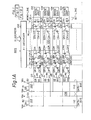
- FIG. 1 shows a MOS DRAM circuit including a data input/output circuit operable in a nibble mode according to the present invention.
- the MOS DRAM circuit includes a memory array 100, an X decoder 102 responsive to a strobe signal RAS for receiving an X address signal to select one of word lines W L of the memory array 100, a plurality of sense amplifiers 104 for amplifying signals from bit lines B of the memory array 100, a timing generator circuit 106 responsive to a strobe signal CAS for receiving a Y address signal to issue control signals ⁇ 1 through ⁇ 10 , and a data input/output circut 108 to control the transmission of data (information) between data input/output terminals and the bit lines B L .
- the timing generator circuit 106 includes a Y address decoder for generating timing signals ⁇ 3 through ⁇ 6 .
- the memory array 100 comprises a plurality of memory cells each composed of a switching MOS transistor Q and a memory capacitor C.
- the data input/output circuit 108 includes a data bus 110 composed of a pair of conductors, switch circuits 114, 118 for selectively coupling the bit lines BLl' B L1 , B L3 , B L3 with the data bus 110 and controlled by the control signals ⁇ 3 and ⁇ 5 , a data bus 112 composed of a pair of conductors, and switch circuits 116, 120 for selectively coupling the bit lines H L2 ' B L2' g L4 , B L4 with the data bus 112 and controlled by the control signals ⁇ 4 and ⁇ 6 .
- Each of these switch circuits 114, 116;118',120 is composed of MOS transistors.
- the data input/output circuit 108 further includes a latch circuit 122 responsive to the control signal ⁇ 9 for amplifying and latching data of the data bus 110, a latch circuit 124 responsive to the control signal ⁇ 10 for amplifying and latching data of the data bus 112, a switch circuit 126 responsive to the control signal ⁇ 7 for issuing the data of the data bus 110, a switch circuit 128 responsive to the control signal ⁇ 8 for issuing the data of the data bus 112, and a data output buffer 130 res- write pensive to an "H"-level/enable signal WE for issuing one of complementary signals from the data bus 110 or one of complementary signals from the data bus 112 to a data output terminal 132.
- the switch circuits 126, 128 are composed of MOS transistors Q 13' Q 14 and Q 15' Q 16' respectively.
- the data input/output circuit 108 also includes a switch circuit 134 connected to the data bus 110 and controlled by the control signal ⁇ 7 a switch circuit 136 connected to the data bus 112 and controlled by the control signal ⁇ 8 , a data input write buffer 138 responsive to an "L"-Ievel/enable signal WE for converting data from a data input terminal 140 into complementary signals and transmitting these complementary signals to the switch circuit 134 or 136, a precharge circuit 142 for charging the data bus 110 up to a power supply potential V DD in response to the control signal ⁇ 1 , and a precharge circuit 144 for charging the data bus 112 up to the power supply potential V DD in response to the control signal ⁇ 2 .
- the switch circuits 134, 136 are composed of MOS transistors Q 17 , Q 18 and Q 19 , Q 20' respectively.
- the precharge circuits 142, 144 are composed of MOS transistors Q 1 , Q 2 and Q 3 , Q 4 , respectively.
- the X address circuit 102 receives the X address signal to select the word line W L1 , for example.
- the sense amplifiers 104 detect and amplify data from the bit lines B L , respectively.
- the Y address signal is applied to the timing generator circuit 106.
- the control signal ⁇ 7 is now caused to change from the "L” level to the "H” level to render the MOS transistors Q 13 ' Q 14 conductive.
- the control signal ⁇ 8 is of the "L” level, the MOS transistors Q 15' Q 16 remain nonconductive.
- control signals ⁇ 1, ⁇ 2 change from the "H” level to the "L” level to render the MOS transistors Q l through Q 4 . nonconductive.
- the control signals ⁇ 3 , ⁇ 4 . change from the "L” level to the "H” level to render the transistors Q 5 .
- Q 6' Q 7 , Q 8 conductive, to.thereby transmit information from the bit lines BL 1 , BL 1 and BL 2 , BL 2 to the data buses 110, 112, respectively.
- the control signals ⁇ 5 , ⁇ 6 are kept in the "L” level to maintain the transistors Q 9 through Q 12 non-conductive.
- the data buses 110, 112 are therefore disconnected from the bit lines BL 3 , BL 3 and BL 4 , BL 4 , respectively. Since the control signals ⁇ 9' ⁇ 10 change from the "L" level to the "H” level, the latch circuits 122, 124 are activated to latch and amplify the data from the data buses 110, 112. At this time, the transistors Q 3' Q 4 are energized, and the data from the data bus 110 is issued through the data output buffer 130 to the data output terminal 132 (see a in FIG. 2(O)).
- the control signal changes from the "L” level to the "H” level, so that the transistors Q 9 , Q 10 are energized to transfer the data from the bit lines B L3' B L3 to the data bus 110.
- the control signal ⁇ 9 changes from the "L” level to the "H” level, activating the latch circuit 122 to latch and amplify the data of the data bus 110.
- the strobe signal CAS goes from the "L” level to the "H” level and the control signal ⁇ 2 goes from the “L” level to the “H” level, whereupon the transistors Q 3 , Q 4 are energized to precharge the data bus 112. Since the control signai ⁇ 4 changes from the "H” level to the “L” level to de-energize the transistors Q 7 , Q 8 , the bit lines B L2 , B L2 are disconnected from the data bus 112. As the control signal ⁇ 10 goes from the "H” level to the "L” level, the latch circuit 124 is reset.
- the control signal ⁇ 7 changes from the "L” level to the "H” level and the control signal ⁇ 8 changes from the "H” level to the “L” level during a period t 6 , with the result that the data from the data bus 110 is issued via the data output buffer 130 to the data output terminal 132 (see c in FIG. 2(0)). Since the control signal ⁇ 6 changes from the "L” level to the "H” Ievel, the transistors Q 11' Q 12 are energized to transfer the data from the bit lines B L4 ' B L4 to the data bus 112. When the control signal ⁇ 10 changes from the "L” level to the "H” level, the latch circuit 124 is activated to latch and amplify the data of the data bus 112.
- the-data items from the data buses 110, 112 are alternately and serially issued to the data output terminal 132 by the control signals ⁇ 3 , ⁇ 4 . ⁇ 5 ' ⁇ 6 and ⁇ 9 ' ⁇ 10'
- FIG. 4 shows flow diagrams of data flow in the readout mode of the data input/output circuit according to the present invention.
- a write mode of-the data input/output circuit of the present invention will be described with reference to FIG. 3.
- an "L"-level/enable signal WE is applied to disenable the data output buffer 130 and enable the data input buffer 138.
- the X address circuit 102 receives an X address signal to select the word line W L1 , for example.
- the sense amplifiers 104 detect and amplify data of the bit lines B L , respectively.
- the control signals ⁇ 1, ⁇ 2 change from the " H " level to the "L” level to de-energize the transistors Q 1 , Q 2 , Q 3 ' Q 4 for thereby interrupting the precharging of the data buses 110, 112. Since the control signals ⁇ 3 , ⁇ 4 go from the "L” level to the "H” level, the bit lines B L1 , B L1 are L1 connected to the data bus 110, and the bit lines BL2, B L2 are connected to the data bus 112. Because the control signal ⁇ 9 is of the.”L" level, the latch circuit 122 is disenabled.
- the control signal ⁇ 10 goes from the "L” level to the "H” level, the latch circuit 124 amplifies the data of the data bus 112 and refreshes information in the memory capacitor C 21 of the bit lines BL2, B L2 . Simultaneously, the information to be written is delivered from the data input buffer 138 onto the data bus 110 and then written in the memory cell of the bit lines B L1 , H L1'
- the strobe signal CAS varies from the "L” level to the "H” level and the control signal ⁇ 1 goes from the “L” level to the “H” level.
- the transistors Q 1 , Q 2 are now energized to precharge the data bus 110 to the power supply potential.
- the control signal ⁇ 3 changes from the "H” level to the "L” level to de-energize the transistors Q 5 , Q 6 thus disconnecting the bit lines B L1' B L1 froar the data bus 110.
- the strobe signal CAS varies from the "H” level to the "L” level and the control signal ⁇ 1 goes from the "H” level to the “L” level, thereby interrupting.the precharging of the data bus 110.
- the data is then introduced from the data input terminal 140 into the data input buffer 138 (see f in FIG. 3(E)).
- the control signal ⁇ 7 goes from the "H” level to the “L” level to de-energize the transistors Q 17 .
- Q 18 ' and simultaneously the control signal ⁇ 8 goes from the "L” level to the "H” level to energize the transistors Q 19 , Q 20 .
- the data from the data input buffer 138 is then delivered to the data bus 112.
- the latch circuit 124 Since the control signal ⁇ 10 goes from the "H” level to the “L” level, the latch circuit 124 is disenabled.
- the control signal ⁇ 4 is of the "H” level for thereby writing the data of the data bus 112 in the memory cell C 21 .
- the control signal ⁇ 5 changes from the "L” level to the “H” level to energize the transistors Q 9 , Q 10 for transferring information from the bit lines BL3, BL3 to the data bus 110.
- the latch circuit 122 Inasmuch as the control signal ⁇ 9 goes from the "L” level to the "H” level, the latch circuit 122 is activated to latch and amplify the information on the data bus 110 and refresh information in the memory capacitor C31.
- the control signal ⁇ 4 changes from the "H” level to the “L” level to de-energize the transistors Q 7 , Q 8 ; the control signal ⁇ 2 goes to the "H” level to precharge the data bus 112; both during a period t 12 ,
- the strobe signal CAS goes from the "H” level to the "L” level to introduce next data from the data input terminal 140 into the data input buffer 138 (see g in FIG. 3(E)).
- the control signal ⁇ 7 goes from the “L” level to the “H” level to energize the transistors Q 17 ' Q 18 ' and simultaneously the control signal ⁇ 8 goes from the "H” level to the “L” level to de-energize the transistors Q 19 .
- Q 20' The data from the data input buffer 138 is then delivered to the data bus 110. Since the control signal ⁇ 5 is of the "H" level at this time, data from the data bus 110 is written into the memory capacitor C 31 of the bit lines B L3 , B L3 .
- the transistors Q 3 , Q 4 are de-energized since the control signal ⁇ 2 goes from the "H” level to the “L” level.
- the control signals ⁇ 6 changes from the “L” level to the “H” level to energize the transistors Q 11 , Q 12' thereby transferring data from the bit lines B L4' B L4 to the data bus 112.
- the latch circuit 124 is activated to latch and amplify the information on the data bus l12 and refresh information in the memory capacitor C 41 .
- data items applied to the data input terminal 140 are transferred alternately to the data buses 110, 112 and written into memory cells.
- the data input/output circuit of the present invention operates in an operation cycle in which, when the first latch circuit connected to the first data bus issues 1-bit information to the data output buffer, next 1-bit information is latched in the second latch circuit connected to the second data bus and simultaneously the first data bus is precharged, and in an operation cycle in which, when 1-bit data stored in the second latch circuit is issued to the data output buffer, next 1-bit data is latched in the first latch circuit and simultaneously the second data bus is precharged.
- the data input/output circuit is advantageous in that, when one of the latch circuits issues data to the data output buffer, the other latch circuit latches data and is in a standby condition, and hence an access time in which to issue data from the bit lines to the data buses is greatly reduced notwithstanding the only two data buses are employed. Accordingly, the chip area occupied by the data buses can be reduced appreciably.
- the data input/output circuit according to the preserit invention is highly effective when used with large-capacity semiconductor DRAM IC devices.
- the data input/output circuit is conducive to miniaturization of IC chips since the number of required data buses can be greatly lowered when issuing serial data from each of a plurality of I/O buffers.
- a large-capacity, high-speed DRAM IC device can be realized according to the present invention without involving an increase in the number of data buses, through timing control of the switch means precharge means, and latch circuits between the bit lines and the data buses.
Landscapes
- Engineering & Computer Science (AREA)
- Computer Hardware Design (AREA)
- Microelectronics & Electronic Packaging (AREA)
- Dram (AREA)
- Static Random-Access Memory (AREA)
Applications Claiming Priority (2)
| Application Number | Priority Date | Filing Date | Title |
|---|---|---|---|
| JP59038758A JPH0787037B2 (ja) | 1984-03-02 | 1984-03-02 | 半導体メモリ回路のデータ書込方法 |
| JP38758/84 | 1984-03-02 |
Publications (3)
| Publication Number | Publication Date |
|---|---|
| EP0154314A2 true EP0154314A2 (fr) | 1985-09-11 |
| EP0154314A3 EP0154314A3 (en) | 1988-05-04 |
| EP0154314B1 EP0154314B1 (fr) | 1991-05-15 |
Family
ID=12534183
Family Applications (1)
| Application Number | Title | Priority Date | Filing Date |
|---|---|---|---|
| EP85102358A Expired - Lifetime EP0154314B1 (fr) | 1984-03-02 | 1985-03-01 | Circuit de données d'entrée et de sortie à densité d'intégration plus élévée pour DRAM |
Country Status (5)
| Country | Link |
|---|---|
| US (1) | US4646272A (fr) |
| EP (1) | EP0154314B1 (fr) |
| JP (1) | JPH0787037B2 (fr) |
| KR (1) | KR910002963B1 (fr) |
| DE (1) | DE3582811D1 (fr) |
Cited By (7)
| Publication number | Priority date | Publication date | Assignee | Title |
|---|---|---|---|---|
| DE3815549A1 (de) * | 1987-05-13 | 1988-12-08 | Mitsubishi Electric Corp | Dynamischer direktzugriffsspeicher |
| DE4118301A1 (de) * | 1990-06-04 | 1991-12-05 | Toshiba Kawasaki Kk | Dynamischer randomspeicher mit synchroner datenuebertragungseinheit |
| EP0409449A3 (en) * | 1989-07-17 | 1992-10-28 | Advanced Micro Devices, Inc. | Interleaved sensing system for fifo and burst-mode memories |
| EP0448025A3 (fr) * | 1990-03-19 | 1994-02-02 | Sharp Kk | |
| EP0588129A3 (fr) * | 1992-08-28 | 1994-12-21 | Tokyo Shibaura Electric Co | Dispositif de mémoire à semi-conducteurs. |
| FR2714514A1 (fr) * | 1993-12-24 | 1995-06-30 | Samsung Electronics Co Ltd | Procédé d'adressage de mémoire et dispositif pour sa mise en Óoeuvre. |
| US5592436A (en) * | 1992-08-28 | 1997-01-07 | Kabushiki Kaisha Toshiba | Data transfer system |
Families Citing this family (14)
| Publication number | Priority date | Publication date | Assignee | Title |
|---|---|---|---|---|
| JPS6212991A (ja) * | 1985-07-10 | 1987-01-21 | Fujitsu Ltd | 半導体記憶装置 |
| US5237532A (en) * | 1986-06-30 | 1993-08-17 | Kabushiki Kaisha Toshiba | Serially-accessed type memory device for providing an interleaved data read operation |
| US4872161A (en) * | 1987-03-19 | 1989-10-03 | Matsushita Electric Industrial Co., Ltd. | Bus circuit for eliminating undesired voltage amplitude |
| JPH0612609B2 (ja) * | 1987-03-27 | 1994-02-16 | 株式会社東芝 | 半導体メモリ |
| JPH01128292A (ja) * | 1987-11-13 | 1989-05-19 | Sanyo Electric Co Ltd | 半導体記憶回路 |
| US4926384A (en) * | 1988-01-25 | 1990-05-15 | Visic, Incorporated | Static ram with write recovery in selected portion of memory array |
| US4878198A (en) * | 1988-01-25 | 1989-10-31 | Visic, Incorporated | Static ram with common data line equalization |
| JPH0283891A (ja) * | 1988-09-20 | 1990-03-23 | Fujitsu Ltd | 半導体メモリ |
| US5305281A (en) * | 1992-08-06 | 1994-04-19 | National Semiconductor Corporation | Multiple array memory device with staggered read/write for high speed data access |
| JPH06231576A (ja) * | 1993-02-04 | 1994-08-19 | Nec Corp | 半導体記憶装置 |
| JPH08273368A (ja) * | 1995-03-28 | 1996-10-18 | Toshiba Microelectron Corp | 半導体記憶装置 |
| KR0167299B1 (ko) * | 1995-12-21 | 1999-02-01 | 문정환 | 메모리의 컬럼스위치 인에이블신호 발생회로 |
| JP3569417B2 (ja) * | 1996-07-19 | 2004-09-22 | 株式会社ルネサステクノロジ | 半導体メモリ |
| JPH11134224A (ja) * | 1997-10-29 | 1999-05-21 | Fujitsu Ltd | 信号観測方法及び信号観測装置 |
Family Cites Families (7)
| Publication number | Priority date | Publication date | Assignee | Title |
|---|---|---|---|---|
| US4330852A (en) * | 1979-11-23 | 1982-05-18 | Texas Instruments Incorporated | Semiconductor read/write memory array having serial access |
| US4344156A (en) * | 1980-10-10 | 1982-08-10 | Inmos Corporation | High speed data transfer for a semiconductor memory |
| JPS581891A (ja) * | 1982-04-23 | 1983-01-07 | Hitachi Ltd | モノリシツク記憶装置 |
| JPS58220294A (ja) * | 1982-06-16 | 1983-12-21 | Mitsubishi Electric Corp | 半導体記憶装置 |
| JPS5956284A (ja) * | 1982-09-24 | 1984-03-31 | Hitachi Micro Comput Eng Ltd | 半導体記憶装置 |
| JPS59116988A (ja) * | 1982-12-24 | 1984-07-06 | Hitachi Ltd | 半導体メモリ装置 |
| US4567579A (en) * | 1983-07-08 | 1986-01-28 | Texas Instruments Incorporated | Dynamic memory with high speed nibble mode |
-
1984
- 1984-03-02 JP JP59038758A patent/JPH0787037B2/ja not_active Expired - Lifetime
-
1985
- 1985-03-01 DE DE8585102358T patent/DE3582811D1/de not_active Expired - Lifetime
- 1985-03-01 EP EP85102358A patent/EP0154314B1/fr not_active Expired - Lifetime
- 1985-03-01 US US06/706,944 patent/US4646272A/en not_active Expired - Lifetime
- 1985-03-02 KR KR1019850001317A patent/KR910002963B1/ko not_active Expired
Cited By (12)
| Publication number | Priority date | Publication date | Assignee | Title |
|---|---|---|---|---|
| DE3815549A1 (de) * | 1987-05-13 | 1988-12-08 | Mitsubishi Electric Corp | Dynamischer direktzugriffsspeicher |
| US5079748A (en) * | 1987-05-13 | 1992-01-07 | Mitsubishi Denki Kabushiki Kaisha | Dynamic random access memory with read-write signal of shortened duration |
| EP0409449A3 (en) * | 1989-07-17 | 1992-10-28 | Advanced Micro Devices, Inc. | Interleaved sensing system for fifo and burst-mode memories |
| EP0448025A3 (fr) * | 1990-03-19 | 1994-02-02 | Sharp Kk | |
| DE4118301A1 (de) * | 1990-06-04 | 1991-12-05 | Toshiba Kawasaki Kk | Dynamischer randomspeicher mit synchroner datenuebertragungseinheit |
| US6108254A (en) * | 1990-06-04 | 2000-08-22 | Kabushiki Kaisha Toshiba | Dynamic random access memory having continuous data line equalization except at address transition during data reading |
| US6337821B1 (en) | 1990-06-04 | 2002-01-08 | Kabushiki Kaisha Toshiba | Dynamic random access memory having continuous data line equalization except at address translation during data reading |
| EP0588129A3 (fr) * | 1992-08-28 | 1994-12-21 | Tokyo Shibaura Electric Co | Dispositif de mémoire à semi-conducteurs. |
| US5508970A (en) * | 1992-08-28 | 1996-04-16 | Kabushiki Kaisha Toshiba | Semiconductor memory device |
| US5592436A (en) * | 1992-08-28 | 1997-01-07 | Kabushiki Kaisha Toshiba | Data transfer system |
| US5706248A (en) * | 1992-08-28 | 1998-01-06 | Kabushiki Kaisha Toshiba | Data transfer system |
| FR2714514A1 (fr) * | 1993-12-24 | 1995-06-30 | Samsung Electronics Co Ltd | Procédé d'adressage de mémoire et dispositif pour sa mise en Óoeuvre. |
Also Published As
| Publication number | Publication date |
|---|---|
| EP0154314B1 (fr) | 1991-05-15 |
| KR850007148A (ko) | 1985-10-30 |
| KR910002963B1 (ko) | 1991-05-11 |
| EP0154314A3 (en) | 1988-05-04 |
| US4646272A (en) | 1987-02-24 |
| JPH0787037B2 (ja) | 1995-09-20 |
| DE3582811D1 (de) | 1991-06-20 |
| JPS60185292A (ja) | 1985-09-20 |
Similar Documents
| Publication | Publication Date | Title |
|---|---|---|
| US4646272A (en) | Data I/O circuit with higher integration density for DRAM | |
| US4567579A (en) | Dynamic memory with high speed nibble mode | |
| US4935896A (en) | Semiconductor memory device having three-transistor type memory cells structure without additional gates | |
| EP0249548B1 (fr) | Dispositif de mémoire à semi-conducteurs à double porte | |
| US4685089A (en) | High speed, low-power nibble mode circuitry for dynamic memory | |
| US5313431A (en) | Multiport semiconductor memory device | |
| US4562555A (en) | Semiconductor memory device | |
| EP0640977B1 (fr) | Mémoire semi-conductrice dynamique avec une unité de cellule statique de mémorisation d'informations | |
| EP0045063A2 (fr) | Dispositif de mémoire | |
| JPS60136086A (ja) | 半導体記憶装置 | |
| KR950000958B1 (ko) | 반도체 메모리 회로 | |
| US4669064A (en) | Semiconductor memory device with improved data write function | |
| WO1980001731A1 (fr) | Organisation dynamique d'une memoire a acces selectif pour la reduction du courant de pointe | |
| KR0167687B1 (ko) | 고속액세스를 위한 데이타 출력패스를 구비하는 반도체 메모리장치 | |
| US4241425A (en) | Organization for dynamic random access memory | |
| US6337821B1 (en) | Dynamic random access memory having continuous data line equalization except at address translation during data reading | |
| GB2264376A (en) | Bit line control in a semiconductor memory device | |
| GB2280975A (en) | Semiconductor memory devices | |
| EP0062547A2 (fr) | Circuit de mémoire | |
| KR880013070A (ko) | 디지탈 신호처리장치 | |
| EP0640976B1 (fr) | Dispositif de mémoire à semi-conducteurs et méthode d'opération | |
| US4485461A (en) | Memory circuit | |
| US6154394A (en) | Data input-output circuit and semiconductor data storage device provided therewith | |
| KR970706577A (ko) | 메모리 시스템내의 페이지 액세스 및 블록전송을 개선하는 회로, 시스템 및 방법(circuits, systems and methods for improving page accesses and block transfers in a memory system) | |
| EP0654790A2 (fr) | Dispositif de mémoire |
Legal Events
| Date | Code | Title | Description |
|---|---|---|---|
| PUAI | Public reference made under article 153(3) epc to a published international application that has entered the european phase |
Free format text: ORIGINAL CODE: 0009012 |
|
| AK | Designated contracting states |
Designated state(s): DE FR GB |
|
| PUAL | Search report despatched |
Free format text: ORIGINAL CODE: 0009013 |
|
| AK | Designated contracting states |
Kind code of ref document: A3 Designated state(s): DE FR GB |
|
| 17P | Request for examination filed |
Effective date: 19880621 |
|
| 17Q | First examination report despatched |
Effective date: 19891124 |
|
| GRAA | (expected) grant |
Free format text: ORIGINAL CODE: 0009210 |
|
| AK | Designated contracting states |
Kind code of ref document: B1 Designated state(s): DE FR GB |
|
| REF | Corresponds to: |
Ref document number: 3582811 Country of ref document: DE Date of ref document: 19910620 |
|
| ET | Fr: translation filed | ||
| PLBE | No opposition filed within time limit |
Free format text: ORIGINAL CODE: 0009261 |
|
| STAA | Information on the status of an ep patent application or granted ep patent |
Free format text: STATUS: NO OPPOSITION FILED WITHIN TIME LIMIT |
|
| 26N | No opposition filed | ||
| REG | Reference to a national code |
Ref country code: GB Ref legal event code: IF02 |
|
| PGFP | Annual fee paid to national office [announced via postgrant information from national office to epo] |
Ref country code: GB Payment date: 20040225 Year of fee payment: 20 |
|
| PGFP | Annual fee paid to national office [announced via postgrant information from national office to epo] |
Ref country code: FR Payment date: 20040309 Year of fee payment: 20 |
|
| PGFP | Annual fee paid to national office [announced via postgrant information from national office to epo] |
Ref country code: DE Payment date: 20040311 Year of fee payment: 20 |
|
| PG25 | Lapsed in a contracting state [announced via postgrant information from national office to epo] |
Ref country code: GB Free format text: LAPSE BECAUSE OF EXPIRATION OF PROTECTION Effective date: 20050228 |
|
| REG | Reference to a national code |
Ref country code: GB Ref legal event code: PE20 |