EP0159199A2 - Méthodes pour fabriquer des dispositifs d'affichage à décharge - Google Patents
Méthodes pour fabriquer des dispositifs d'affichage à décharge Download PDFInfo
- Publication number
- EP0159199A2 EP0159199A2 EP85302739A EP85302739A EP0159199A2 EP 0159199 A2 EP0159199 A2 EP 0159199A2 EP 85302739 A EP85302739 A EP 85302739A EP 85302739 A EP85302739 A EP 85302739A EP 0159199 A2 EP0159199 A2 EP 0159199A2
- Authority
- EP
- European Patent Office
- Prior art keywords
- lab
- layer
- conductive paste
- cathode
- glass binder
- Prior art date
- Legal status (The legal status is an assumption and is not a legal conclusion. Google has not performed a legal analysis and makes no representation as to the accuracy of the status listed.)
- Granted
Links
Images
Classifications
-
- H—ELECTRICITY
- H01—ELECTRIC ELEMENTS
- H01J—ELECTRIC DISCHARGE TUBES OR DISCHARGE LAMPS
- H01J11/00—Gas-filled discharge tubes with alternating current induction of the discharge, e.g. alternating current plasma display panels [AC-PDP]; Gas-filled discharge tubes without any main electrode inside the vessel; Gas-filled discharge tubes with at least one main electrode outside the vessel
- H01J11/20—Constructional details
- H01J11/22—Electrodes, e.g. special shape, material or configuration
-
- H—ELECTRICITY
- H01—ELECTRIC ELEMENTS
- H01J—ELECTRIC DISCHARGE TUBES OR DISCHARGE LAMPS
- H01J9/00—Apparatus or processes specially adapted for the manufacture, installation, removal, maintenance of electric discharge tubes, discharge lamps, or parts thereof; Recovery of material from discharge tubes or lamps
- H01J9/02—Manufacture of electrodes or electrode systems
-
- H—ELECTRICITY
- H01—ELECTRIC ELEMENTS
- H01J—ELECTRIC DISCHARGE TUBES OR DISCHARGE LAMPS
- H01J11/00—Gas-filled discharge tubes with alternating current induction of the discharge, e.g. alternating current plasma display panels [AC-PDP]; Gas-filled discharge tubes without any main electrode inside the vessel; Gas-filled discharge tubes with at least one main electrode outside the vessel
- H01J11/20—Constructional details
- H01J11/22—Electrodes, e.g. special shape, material or configuration
- H01J11/32—Disposition of the electrodes
-
- H—ELECTRICITY
- H01—ELECTRIC ELEMENTS
- H01J—ELECTRIC DISCHARGE TUBES OR DISCHARGE LAMPS
- H01J17/00—Gas-filled discharge tubes with solid cathode
- H01J17/02—Details
- H01J17/04—Electrodes; Screens
- H01J17/06—Cathodes
Definitions
- This invention relates to methods of producing discharge display devices.
- Nickel (Ni) is conventionally used as an anode and a cathode. Ni has little resistance against discharge sputtering, and a Ni cathode therefore deteriorates in several seconds of operation.
- mercury (Hg) has been sealed in the discharge display panel and deposited on a surface of the electrode to suppress sputtering.
- mercury (Hg) is sealed in the discharge display panel, it is difficult to maintain the discharge characteristics of each display cell uniform over a long time in a discharge display panel of large capacity, as non-uniform distribution of the mercury occurs due to change on standing.
- LaB 6 Lanthanum boride (LaB 6 ) had been proposed as a cathode material.
- LaB 6 has the advantages that its work function is low ( X coefficient is large) and its discharge efficiency is high; and it is superior in physical and chemical stability due to its covalent bonding structure.
- an LaB 6 cathode has not yet reached practical use for the reason that its usual production process, employing a thin-film evaporation method or a plasma spraying method, is complicated and results in an increase in cost.
- it is difficult to form a relatively uniform electrode with a large capacity and a large screen.
- Another reason is that the electrode cannot be formed in connection with the other panel structure by a thick-film printing method at low cost.
- an LaB6 cathode In the case where an LaB6 cathode is intended to be formed by the thick-film printing method, it is generally burnt in an atmosphere of nitrogen (N 2 ) at 800°C to 900°C after printing and application. However, since a substrate of the discharge display panel is glass, the temperature is permitted to be raised up only to about 600°C, and since a structure such as the other electrodes and barrier is of oxide, such a burning step is usually carried out in air. For these reasons, it is difficult to form the LaB 6 cathode.
- N 2 nitrogen
- LaB 6 has a high melting point of about 2300°C, and therefore it cannot be sintered at a temperature of about 600°C, with a result that the resistance after formation of the cathode is disadvantageously increased to 10 9 ohms or more.
- a binder substance such as frit glass is generally mixed with LaB 6 powder so as to obtain bonding strength between the LaB 6 powder particles.
- glass binder mixed with LaB 6 powder since it causes high resistance after formation of the LaB 6 cathode.
- an LaB 6 cathode which enables the LaB6 cathode to be formed by a thick-film printing method. See our copending related EPC Patent Application No85302738. (Publication No ) corresponding to Japanese Patent Application No 59/79216. According to that method, an LaB 6 paste is prepared by using an ionic conductive alkali glass as a glass binder, the LaB 6 paste is applied and printed onto a base electrode such as Ni, and the paste thereafter is burnt in air at 500°C to 600°C.
- glass binder is not contained in the LaB 6 paste. This is due to the fact that, since the surface of the LaB 6 particles and the space therebetween is covered or filled with glass binder, it is difficult to form an electrical conductive path, resulting in difficulty in activation of the electrodes, and that, in the event of using a frit glass containing lead (Pb) as the binder, there is a possibility that the life endurance characteristic will be reduced by sputtering of metallic Pb as deposited.
- a method of producing a discharge display device comprising the steps of applying a conductive paste containing a glass binder, temporarily drying the conductive paste, applying and printing an LaB 6 paste onto the conductive paste layer or electodepositing LaB 6 containing no glass binder to form an LaB 6 layer, buring the conductive paste layer and the LaB 6 layer at the same time, and activating the LaB 6 layer after it has been burnt by gas discharge with a large current after an exhaustion step to form an LaB 6 cathode.
- a method of producing a discharge display device comprising the steps of applying to a dielectric substrate a conductive paste containing a glass binder to form a conductive paste layer, temporarily drying the conductive paste layer, forming an LaB 6 layer containing no glass binder on the conductive paste layer, burning the conductive paste layer and the LaB 6 layer at the same time, and activating the LaB 6 layer after being burnt by gas discharge with a large current after an exhaustion step to form an LaB 6 cathode.
- a preferred embodiment of the present invention described hereinbelow provides a method of producing a discharge display device which enables formation of a satisfactory LaB 6 cathode without using an La8 6 paste containing a glass binder.
- the preferred method it is possible to form an LaB 6 cathode having a large adhesive strength, and easily effect activation treatment upon formation of the LaB 6 cathode.
- the LaB 6 layer containing no glass binder is formed on the temporarily dried conductive paste layer, and both the LaB 6 layer and the conductive paste layer are burnt simultaneously.
- a part of the glass binder in the conductive paste layer is wetted and migrates into the LaB 6 layer. Accordingly, it is possible to form a satisfactory LaB 6 cathode having a large adhesive strength without using an LaB 6 paste containing a glass binder.
- the activation step may be carried out easily. Additionally, since the amount of the glass binder to be scattered upon activation becomes small, the life of the discharge display device may be further improved.
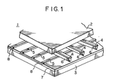
- the discharge display device is a direct current type discharge display panel 1 of a trigger discharge system.
- the discharge panel 1 comprises a front glass substrate 2, a rear glass substrate 3, and anodes 4 and cathodes 5 of XY matrix shape.
- the anodes 4 are partitioned from each other by insulative barriers 6.
- Trigger electrodes 8, formed of aluminium (Al), for example, are arranged on the rear glass substrate 3 in parallel relation with the cathodes 5, an insulative dielectric layer 7 being disposed under the cathodes 5.
- the display panel 1 is manufactured in the following manner. First, the anodes 4 and the insulative barriers 6 are formed on the front glass substrate 2 by a thick-film printing method. Similarly, the trigger electrodes 8, the insulative dielectric layer 7 and the cathodes 5 are formed sequentially on the rear glass substrate 3 by the thick-film printing method. Each of these parts is burnt atter printing. then, the glass substrates 2 and 3 are arranged in opposition to one another, with the anodes 4 and the cathodes 5 crossing at right angles, and are frit-sealed. Thereafter, heating exhaustion, gas sealing (for example, Ne-Ar gas) and final sealing are carried out to complete the display panel 1.
- gas sealing for example, Ne-Ar gas
- a driving voltage is applied selectively to the anodes 4 and the cathodes 5 to generate discharge luminescence at crossing points between the selected anodes 4 and cathodes 5, thereby effecting display in a linearly sequential manner.
- a trigger voltage is applied to the trigger electrodes 8 prior to effecting discharge between the anodes 4 and the cathodes 5 to induce a wall voltage on a portion of the insulative dielectric layer 7 corresponding to the trigger electrodes 8 and effect momentary discharge between the insulative dielectric layer 7 and the selected cathodes 5.
- a gas space along the cathodes5 is ionised, so that subsequent discharge between the selected anodes 4 and cathodes 5 may be effected easily.
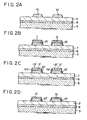
- a preferred embodiment of the present invention described below with reference to Figures 2A to 2D is directed to a method of forming the cathodes 5 in the discharge display panel by the thick-film printing method.
- an LaB 6 paste comprising only fine LaBS powder and a suitable vehicle (solvent) is prepared as a preliminary step without using a glass binder.
- sintered LaB 6 powder as roughly pulverised is further pulverised by a ball mill to prepare a fine LaB 6 powder.
- the fine LaBS powder is selected in such a manner that an average particle size thereof is not more than several micrometres, preferably 1 to 3 micrometres, and powder having an average particle size of not less than 5 micrometres is present in a proportion of not more than 5% with respect to the total amount of LaB 6 powder.
- the fine LaB 6 powder is prepared, it is washed with pure water for the purpose of removing impurities, and is then mixed with the vehicle to prepare an LaB6 paste.
- the trigger electrode 8 and the insulative dielectric layer 7 are first formed on the rear glass substrate 3, and then a conductive paste such as a Ni paste containing a glass binder is applied and printed along a cathode pattern to be formed on the insulative dielectric layer 7 to form Ni paste layers 10.
- the Ni paste layers 10 subsequently serve as base electrodes for supplying current.
- the Ni paste layers 10 are dried, and then the LaB 6 paste is applied onto the Ni paste layers 10 to form L B B 6 layers 11.
- the LaB 6 paste layers 11 are dried, and both the Ni paste layers 10 and the LaB 6 paste layers 11 are burnt simultaneously under such conditions as in air at 500°C to 600°C, for example about 560 C.
- Ni base layers 10' are formed.
- a part of the glass binder contained in the Ni paste layers 10 is wetted and migrates into LaB 6 layers 11'. Due to wetting of the glass binder, LaB 6 layers lla' as wetted by the glass binder are increased in bonding strength between the Ni base layers 10' and the LaB 6 layers 11' as well as between each of the LaB6 particles.
- LaB 6 cathodes 12 are formed on the Ni base electrodes 10'.
- the LaB 6 paste layers 11 containing no glass binder are applied and printed onto the Ni paste base layers 10 as temporarily dried, and then both the layers 10 and 11 are burnt simultaneously, thereby permitting a part of the glass binder contained in the Ni paste layers 10 to be wetted into the LaB 6 layers 11'. Accordingly, due to such wetting of the glass binder, it is possible finally to obtain LaB 6 cathodes 12 having a large adhesive strength.
- the amount of the glass binder to be contained in the LaB 6 layers 11' is small, the amount of the glass binder to be scattered upon activation by gas discharge with a large current also is small, thereby reducing negative influence due to scatter of the glass binder, resulting in improvement to the life of the discharge display device.
- a satisfactory LaB 6 cathode may be formed by the thick-film printing method.
- LaB 6 paste containing no glass binder is applied and printed onto the Ni paste base layer in the preferred embodiment, it is also possible to form an LaB 6 layer on the Ni paste layer by an electrodeposition method or the like in substitution for the LaB 6 paste.
Landscapes
- Engineering & Computer Science (AREA)
- Manufacturing & Machinery (AREA)
- Chemical & Material Sciences (AREA)
- Materials Engineering (AREA)
- Physics & Mathematics (AREA)
- Plasma & Fusion (AREA)
- Gas-Filled Discharge Tubes (AREA)
Applications Claiming Priority (2)
| Application Number | Priority Date | Filing Date | Title |
|---|---|---|---|
| JP79218/84 | 1984-04-19 | ||
| JP59079218A JPS60221928A (ja) | 1984-04-19 | 1984-04-19 | 放電表示装置の製造方法 |
Publications (3)
| Publication Number | Publication Date |
|---|---|
| EP0159199A2 true EP0159199A2 (fr) | 1985-10-23 |
| EP0159199A3 EP0159199A3 (en) | 1987-04-29 |
| EP0159199B1 EP0159199B1 (fr) | 1990-03-14 |
Family
ID=13683782
Family Applications (1)
| Application Number | Title | Priority Date | Filing Date |
|---|---|---|---|
| EP85302739A Expired - Lifetime EP0159199B1 (fr) | 1984-04-19 | 1985-04-18 | Méthodes pour fabriquer des dispositifs d'affichage à décharge |
Country Status (6)
| Country | Link |
|---|---|
| US (1) | US4600397A (fr) |
| EP (1) | EP0159199B1 (fr) |
| JP (1) | JPS60221928A (fr) |
| KR (1) | KR930001175B1 (fr) |
| CA (1) | CA1240360A (fr) |
| DE (1) | DE3576606D1 (fr) |
Cited By (3)
| Publication number | Priority date | Publication date | Assignee | Title |
|---|---|---|---|---|
| WO1998059355A3 (fr) * | 1997-06-24 | 1999-06-10 | Nikolai Nikolaevich Dzbanovsky | Cathode froide et procedes de fabrication |
| RU2158037C2 (ru) * | 1996-07-16 | 2000-10-20 | ООО "Высокие технологии" | Способ получения алмазных пленок методом газофазного синтеза |
| RU2158036C2 (ru) * | 1996-02-29 | 2000-10-20 | ООО "Высокие технологии" | Способ получения алмазных пленок методом газофазного синтеза |
Families Citing this family (10)
| Publication number | Priority date | Publication date | Assignee | Title |
|---|---|---|---|---|
| JPS61284030A (ja) * | 1985-06-10 | 1986-12-15 | Hitachi Ltd | 気体放電表示パネル用陰極 |
| JPS6445037A (en) * | 1987-08-14 | 1989-02-17 | Yoshifumi Amano | Manufacture of cathode device in discharge display element |
| JPS6489242A (en) * | 1987-09-30 | 1989-04-03 | Mitsubishi Electric Corp | Electrode for discharge light source |
| JPH0264133U (fr) * | 1988-11-01 | 1990-05-14 | ||
| US5209688A (en) * | 1988-12-19 | 1993-05-11 | Narumi China Corporation | Plasma display panel |
| US5468169A (en) * | 1991-07-18 | 1995-11-21 | Motorola | Field emission device employing a sequential emitter electrode formation method |
| TW368671B (en) * | 1995-08-30 | 1999-09-01 | Tektronix Inc | Sputter-resistant, low-work-function, conductive coatings for cathode electrodes in DC plasma addressing structure |
| US6077617A (en) * | 1998-08-26 | 2000-06-20 | Board Of Regents Of The University Of Nebraska | Rare-earth boride thin film system |
| US6025038A (en) * | 1998-08-26 | 2000-02-15 | Board Of Regents Of The University Of Nebraska | Method for depositing rare-earth boride onto a substrate |
| DE19841900A1 (de) * | 1998-09-11 | 2000-03-30 | Schott Glas | Verfahren zum Aufbringen von metallischen Leiterbahnen als Elektroden auf eine Kanalplatte für großflächige Flachbildschirme |
Family Cites Families (6)
| Publication number | Priority date | Publication date | Assignee | Title |
|---|---|---|---|---|
| US2172207A (en) * | 1936-09-19 | 1939-09-05 | Siemens Ag | Glow cathode |
| US4126809A (en) * | 1975-03-10 | 1978-11-21 | Owens-Illinois, Inc. | Gas discharge display panel with lanthanide or actinide family oxide |
| FR2445605A1 (fr) * | 1978-12-27 | 1980-07-25 | Thomson Csf | Cathode a chauffage direct et tube electronique haute frequence comportant une telle cathode |
| US4393326A (en) * | 1980-02-22 | 1983-07-12 | Okaya Electric Industries Co., Ltd. | DC Plasma display panel |
| US4317750A (en) * | 1980-08-22 | 1982-03-02 | Ferro Corporation | Thick film conductor employing nickel oxide |
| JPS57180046A (en) * | 1981-04-28 | 1982-11-05 | Okaya Denki Sangyo Kk | Panel for displaying dc gas discharge |
-
1984
- 1984-04-19 JP JP59079218A patent/JPS60221928A/ja active Pending
-
1985
- 1985-04-11 US US06/721,956 patent/US4600397A/en not_active Expired - Fee Related
- 1985-04-11 CA CA000478803A patent/CA1240360A/fr not_active Expired
- 1985-04-16 KR KR1019850002553A patent/KR930001175B1/ko not_active Expired - Fee Related
- 1985-04-18 EP EP85302739A patent/EP0159199B1/fr not_active Expired - Lifetime
- 1985-04-18 DE DE8585302739T patent/DE3576606D1/de not_active Expired - Lifetime
Cited By (5)
| Publication number | Priority date | Publication date | Assignee | Title |
|---|---|---|---|---|
| RU2158036C2 (ru) * | 1996-02-29 | 2000-10-20 | ООО "Высокие технологии" | Способ получения алмазных пленок методом газофазного синтеза |
| RU2158037C2 (ru) * | 1996-07-16 | 2000-10-20 | ООО "Высокие технологии" | Способ получения алмазных пленок методом газофазного синтеза |
| WO1998059355A3 (fr) * | 1997-06-24 | 1999-06-10 | Nikolai Nikolaevich Dzbanovsky | Cathode froide et procedes de fabrication |
| RU2161838C2 (ru) * | 1997-06-24 | 2001-01-10 | Тарис Технолоджис, Инк. | Холодноэмиссионный пленочный катод и способы его получения |
| US6593683B1 (en) | 1997-06-24 | 2003-07-15 | Obschestvo s ogranichennoy otvetstvennostyu “Vysokie Tekhnologii” | Cold cathode and methods for producing the same |
Also Published As
| Publication number | Publication date |
|---|---|
| CA1240360A (fr) | 1988-08-09 |
| JPS60221928A (ja) | 1985-11-06 |
| EP0159199A3 (en) | 1987-04-29 |
| KR850007531A (ko) | 1985-12-04 |
| KR930001175B1 (ko) | 1993-02-20 |
| EP0159199B1 (fr) | 1990-03-14 |
| US4600397A (en) | 1986-07-15 |
| DE3576606D1 (de) | 1990-04-19 |
Similar Documents
| Publication | Publication Date | Title |
|---|---|---|
| EP0160459B1 (fr) | Méthodes pour fabriquer des dispositifs d'affichage à décharge | |
| US4393326A (en) | DC Plasma display panel | |
| US5557168A (en) | Gas-discharging type display device and a method of manufacturing | |
| EP0159199B1 (fr) | Méthodes pour fabriquer des dispositifs d'affichage à décharge | |
| KR880012122A (ko) | 개선된 형성을 위한 중간층을 지닌 전기발광표시 및 그의 제조방법 | |
| US4746838A (en) | Ink for forming resistive structures and display panel containing the same | |
| KR970012899A (ko) | 스퍼터내성이 있고,일함수가 낮은 도전성 재료로 코팅된 직류 플라즈마어드레싱구조의 캐소드전극 | |
| US5914559A (en) | Resistance element and cathode ray tube | |
| US5159238A (en) | Gas discharge panel | |
| JP2525280B2 (ja) | 隔壁中の有孔金属板を電極としたプラズマディスプレイパネル | |
| JPH071673B2 (ja) | ガス放電型表示パネルの製造方法 | |
| JPH0495332A (ja) | 放電電極 | |
| US6184616B1 (en) | Resistor electron gun for cathode-ray tube using the same and method of manufacturing resistor | |
| JP2769933B2 (ja) | 直流型放電表示管およびその陰極形成用組成物 | |
| JPH0785800A (ja) | ガス放電表示パネルの陰極及びその作成方法 | |
| JP3016537B2 (ja) | 表示放電管用冷陰極の製造方法 | |
| JP3519371B2 (ja) | 蛍光表示管 | |
| DE69504572T2 (de) | Bildanzeigegerät und Verfahren zur Herstellung desselben | |
| JPH01272028A (ja) | ガス放電表示パネルの電極形成方法 | |
| JPH01225040A (ja) | 電子放出用電極及び表示装置 | |
| JPH04236269A (ja) | 導電性コーティング材料 | |
| JP3535059B2 (ja) | プラズマ表示装置用基板 | |
| JPS60221927A (ja) | 放電表示装置の製造方法 | |
| JPH0778566A (ja) | ガス放電表示パネル及びその形成方法 | |
| JP2000298261A (ja) | プラズマアドレス液晶表示装置 |
Legal Events
| Date | Code | Title | Description |
|---|---|---|---|
| PUAI | Public reference made under article 153(3) epc to a published international application that has entered the european phase |
Free format text: ORIGINAL CODE: 0009012 |
|
| AK | Designated contracting states |
Designated state(s): DE FR GB IT |
|
| PUAL | Search report despatched |
Free format text: ORIGINAL CODE: 0009013 |
|
| AK | Designated contracting states |
Kind code of ref document: A3 Designated state(s): DE FR GB IT |
|
| 17P | Request for examination filed |
Effective date: 19870925 |
|
| 17Q | First examination report despatched |
Effective date: 19881117 |
|
| GRAA | (expected) grant |
Free format text: ORIGINAL CODE: 0009210 |
|
| AK | Designated contracting states |
Kind code of ref document: B1 Designated state(s): DE FR GB IT |
|
| ITF | It: translation for a ep patent filed | ||
| REF | Corresponds to: |
Ref document number: 3576606 Country of ref document: DE Date of ref document: 19900419 |
|
| ET | Fr: translation filed | ||
| PLBE | No opposition filed within time limit |
Free format text: ORIGINAL CODE: 0009261 |
|
| STAA | Information on the status of an ep patent application or granted ep patent |
Free format text: STATUS: NO OPPOSITION FILED WITHIN TIME LIMIT |
|
| 26N | No opposition filed | ||
| ITTA | It: last paid annual fee | ||
| PGFP | Annual fee paid to national office [announced via postgrant information from national office to epo] |
Ref country code: GB Payment date: 19950410 Year of fee payment: 11 Ref country code: DE Payment date: 19950410 Year of fee payment: 11 |
|
| PGFP | Annual fee paid to national office [announced via postgrant information from national office to epo] |
Ref country code: FR Payment date: 19950411 Year of fee payment: 11 |
|
| PG25 | Lapsed in a contracting state [announced via postgrant information from national office to epo] |
Ref country code: GB Effective date: 19960418 |
|
| GBPC | Gb: european patent ceased through non-payment of renewal fee |
Effective date: 19960418 |
|
| PG25 | Lapsed in a contracting state [announced via postgrant information from national office to epo] |
Ref country code: FR Effective date: 19961227 |
|
| PG25 | Lapsed in a contracting state [announced via postgrant information from national office to epo] |
Ref country code: DE Effective date: 19970101 |
|
| REG | Reference to a national code |
Ref country code: FR Ref legal event code: ST |