EP0177864B1 - Dispositif semi-conducteur à multi-jonction - Google Patents
Dispositif semi-conducteur à multi-jonction Download PDFInfo
- Publication number
- EP0177864B1 EP0177864B1 EP85112318A EP85112318A EP0177864B1 EP 0177864 B1 EP0177864 B1 EP 0177864B1 EP 85112318 A EP85112318 A EP 85112318A EP 85112318 A EP85112318 A EP 85112318A EP 0177864 B1 EP0177864 B1 EP 0177864B1
- Authority
- EP
- European Patent Office
- Prior art keywords
- layer
- metal
- silicide
- semiconductor
- diffusion
- Prior art date
- Legal status (The legal status is an assumption and is not a legal conclusion. Google has not performed a legal analysis and makes no representation as to the accuracy of the status listed.)
- Expired - Lifetime
Links
Images

Classifications
-
- H—ELECTRICITY
- H10—SEMICONDUCTOR DEVICES; ELECTRIC SOLID-STATE DEVICES NOT OTHERWISE PROVIDED FOR
- H10F—INORGANIC SEMICONDUCTOR DEVICES SENSITIVE TO INFRARED RADIATION, LIGHT, ELECTROMAGNETIC RADIATION OF SHORTER WAVELENGTH OR CORPUSCULAR RADIATION
- H10F10/00—Individual photovoltaic cells, e.g. solar cells
- H10F10/10—Individual photovoltaic cells, e.g. solar cells having potential barriers
- H10F10/17—Photovoltaic cells having only PIN junction potential barriers
- H10F10/172—Photovoltaic cells having only PIN junction potential barriers comprising multiple PIN junctions, e.g. tandem cells
-
- H—ELECTRICITY
- H10—SEMICONDUCTOR DEVICES; ELECTRIC SOLID-STATE DEVICES NOT OTHERWISE PROVIDED FOR
- H10D—INORGANIC ELECTRIC SEMICONDUCTOR DEVICES
- H10D8/00—Diodes
- H10D8/50—PIN diodes
-
- H—ELECTRICITY
- H10—SEMICONDUCTOR DEVICES; ELECTRIC SOLID-STATE DEVICES NOT OTHERWISE PROVIDED FOR
- H10F—INORGANIC SEMICONDUCTOR DEVICES SENSITIVE TO INFRARED RADIATION, LIGHT, ELECTROMAGNETIC RADIATION OF SHORTER WAVELENGTH OR CORPUSCULAR RADIATION
- H10F71/00—Manufacture or treatment of devices covered by this subclass
- H10F71/10—Manufacture or treatment of devices covered by this subclass the devices comprising amorphous semiconductor material
- H10F71/103—Manufacture or treatment of devices covered by this subclass the devices comprising amorphous semiconductor material including only Group IV materials
-
- H—ELECTRICITY
- H10—SEMICONDUCTOR DEVICES; ELECTRIC SOLID-STATE DEVICES NOT OTHERWISE PROVIDED FOR
- H10F—INORGANIC SEMICONDUCTOR DEVICES SENSITIVE TO INFRARED RADIATION, LIGHT, ELECTROMAGNETIC RADIATION OF SHORTER WAVELENGTH OR CORPUSCULAR RADIATION
- H10F77/00—Constructional details of devices covered by this subclass
- H10F77/10—Semiconductor bodies
- H10F77/16—Material structures, e.g. crystalline structures, film structures or crystal plane orientations
- H10F77/162—Non-monocrystalline materials, e.g. semiconductor particles embedded in insulating materials
- H10F77/166—Amorphous semiconductors
-
- H—ELECTRICITY
- H10—SEMICONDUCTOR DEVICES; ELECTRIC SOLID-STATE DEVICES NOT OTHERWISE PROVIDED FOR
- H10W—GENERIC PACKAGES, INTERCONNECTIONS, CONNECTORS OR OTHER CONSTRUCTIONAL DETAILS OF DEVICES COVERED BY CLASS H10
- H10W90/00—Package configurations
-
- H—ELECTRICITY
- H10—SEMICONDUCTOR DEVICES; ELECTRIC SOLID-STATE DEVICES NOT OTHERWISE PROVIDED FOR
- H10W—GENERIC PACKAGES, INTERCONNECTIONS, CONNECTORS OR OTHER CONSTRUCTIONAL DETAILS OF DEVICES COVERED BY CLASS H10
- H10W90/00—Package configurations
- H10W90/701—Package configurations characterised by the relative positions of pads or connectors relative to package parts
- H10W90/731—Package configurations characterised by the relative positions of pads or connectors relative to package parts of die-attach connectors
- H10W90/732—Package configurations characterised by the relative positions of pads or connectors relative to package parts of die-attach connectors between stacked chips
-
- Y—GENERAL TAGGING OF NEW TECHNOLOGICAL DEVELOPMENTS; GENERAL TAGGING OF CROSS-SECTIONAL TECHNOLOGIES SPANNING OVER SEVERAL SECTIONS OF THE IPC; TECHNICAL SUBJECTS COVERED BY FORMER USPC CROSS-REFERENCE ART COLLECTIONS [XRACs] AND DIGESTS
- Y02—TECHNOLOGIES OR APPLICATIONS FOR MITIGATION OR ADAPTATION AGAINST CLIMATE CHANGE
- Y02E—REDUCTION OF GREENHOUSE GAS [GHG] EMISSIONS, RELATED TO ENERGY GENERATION, TRANSMISSION OR DISTRIBUTION
- Y02E10/00—Energy generation through renewable energy sources
- Y02E10/50—Photovoltaic [PV] energy
- Y02E10/548—Amorphous silicon PV cells
-
- Y—GENERAL TAGGING OF NEW TECHNOLOGICAL DEVELOPMENTS; GENERAL TAGGING OF CROSS-SECTIONAL TECHNOLOGIES SPANNING OVER SEVERAL SECTIONS OF THE IPC; TECHNICAL SUBJECTS COVERED BY FORMER USPC CROSS-REFERENCE ART COLLECTIONS [XRACs] AND DIGESTS
- Y02—TECHNOLOGIES OR APPLICATIONS FOR MITIGATION OR ADAPTATION AGAINST CLIMATE CHANGE
- Y02P—CLIMATE CHANGE MITIGATION TECHNOLOGIES IN THE PRODUCTION OR PROCESSING OF GOODS
- Y02P70/00—Climate change mitigation technologies in the production process for final industrial or consumer products
- Y02P70/50—Manufacturing or production processes characterised by the final manufactured product
Definitions
- a layer of metal silicide is formed by depositing a metal silicide compound by means of electron-beam-evaporation or sputtering.
- a metal silicide compound by means of electron-beam-evaporation or sputtering.
- another method can also be employed wherein a metal is deposited by the use of a sputtering target and simultaneously silicon is deposited by glow-discharge decomposition.
- Co-sputtering process can also be employed for deposition of the layer, wherein sputtering of metal and sputtering of silicon are carried out simultaneously.
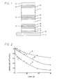
- a heat-resistant multijunction semiconductor device having a diffusion-blocking layer between p-layer and n-layer of the semiconductor device.
- the diffusion-blocking layer prevents dopant atoms in the p-layer and the n-layer, respectively, from diffusing into the other layer.
- the characteristics of the semiconductor device of the invention are not lowered even at a high temperature. Therefore, the semiconductor device of the invention is effectively applied to a solar cell which is used at a high temperature.
Landscapes
- Photovoltaic Devices (AREA)
- Bipolar Transistors (AREA)
- Junction Field-Effect Transistors (AREA)
- Semiconductor Integrated Circuits (AREA)
- Internal Circuitry In Semiconductor Integrated Circuit Devices (AREA)
- Electrodes Of Semiconductors (AREA)
Claims (11)
Priority Applications (1)
| Application Number | Priority Date | Filing Date | Title |
|---|---|---|---|
| AT85112318T ATE59116T1 (de) | 1984-10-11 | 1985-09-28 | Halbleiteranordnung mit mehreren uebergaengen. |
Applications Claiming Priority (2)
| Application Number | Priority Date | Filing Date | Title |
|---|---|---|---|
| JP59213944A JPS6191974A (ja) | 1984-10-11 | 1984-10-11 | 耐熱性マルチジヤンクシヨン型半導体素子 |
| JP213944/84 | 1984-10-11 |
Publications (3)
| Publication Number | Publication Date |
|---|---|
| EP0177864A2 EP0177864A2 (fr) | 1986-04-16 |
| EP0177864A3 EP0177864A3 (en) | 1987-03-25 |
| EP0177864B1 true EP0177864B1 (fr) | 1990-12-12 |
Family
ID=16647630
Family Applications (1)
| Application Number | Title | Priority Date | Filing Date |
|---|---|---|---|
| EP85112318A Expired - Lifetime EP0177864B1 (fr) | 1984-10-11 | 1985-09-28 | Dispositif semi-conducteur à multi-jonction |
Country Status (10)
| Country | Link |
|---|---|
| US (1) | US4907052A (fr) |
| EP (1) | EP0177864B1 (fr) |
| JP (1) | JPS6191974A (fr) |
| KR (1) | KR950001956B1 (fr) |
| CN (1) | CN1003027B (fr) |
| AT (1) | ATE59116T1 (fr) |
| AU (1) | AU589568B2 (fr) |
| CA (1) | CA1252229A (fr) |
| DE (1) | DE3580891D1 (fr) |
| RU (1) | RU2050632C1 (fr) |
Families Citing this family (42)
| Publication number | Priority date | Publication date | Assignee | Title |
|---|---|---|---|---|
| JPS63503103A (ja) * | 1985-09-30 | 1988-11-10 | 鐘淵化学工業株式会社 | マルチジャンクション型半導体デバイス |
| JPS6366976A (ja) * | 1986-09-08 | 1988-03-25 | Semiconductor Energy Lab Co Ltd | 光電変換半導体装置 |
| JPS6350149U (fr) * | 1986-09-19 | 1988-04-05 | ||
| JPS6384075A (ja) * | 1986-09-26 | 1988-04-14 | Sanyo Electric Co Ltd | 光起電力装置 |
| JPS63100858U (fr) * | 1986-12-19 | 1988-06-30 | ||
| JPS63157484A (ja) * | 1986-12-22 | 1988-06-30 | Kanegafuchi Chem Ind Co Ltd | 半導体装置 |
| JPH07114292B2 (ja) * | 1986-12-22 | 1995-12-06 | 鐘淵化学工業株式会社 | 半導体装置及びその製法 |
| JPS63157483A (ja) * | 1986-12-22 | 1988-06-30 | Kanegafuchi Chem Ind Co Ltd | 半導体装置 |
| JPH01128477A (ja) * | 1987-11-12 | 1989-05-22 | Ricoh Co Ltd | アモルファスシリコン光センサー |
| US5021849A (en) * | 1989-10-30 | 1991-06-04 | Motorola, Inc. | Compact SRAM cell with polycrystalline silicon diode load |
| US5151387A (en) | 1990-04-30 | 1992-09-29 | Sgs-Thomson Microelectronics, Inc. | Polycrystalline silicon contact structure |
| US5432129A (en) * | 1993-04-29 | 1995-07-11 | Sgs-Thomson Microelectronics, Inc. | Method of forming low resistance contacts at the junction between regions having different conductivity types |
| KR100275715B1 (ko) * | 1993-12-28 | 2000-12-15 | 윤종용 | 수소화 효과 증대를 위한 반도체 소자의 제조 방법 |
| US5624869A (en) * | 1994-04-13 | 1997-04-29 | International Business Machines Corporation | Method of forming a film for a multilayer Semiconductor device for improving thermal stability of cobalt silicide using platinum or nitrogen |
| US6197628B1 (en) * | 1998-08-27 | 2001-03-06 | Micron Technology, Inc. | Ruthenium silicide diffusion barrier layers and methods of forming same |
| DE102005013537A1 (de) * | 2004-03-24 | 2005-10-20 | Sharp Kk | Fotoelektrischer Wandler und Herstellverfahren für einen solchen |
| US10374120B2 (en) * | 2005-02-18 | 2019-08-06 | Koninklijke Philips N.V. | High efficiency solar cells utilizing wafer bonding and layer transfer to integrate non-lattice matched materials |
| US8203071B2 (en) | 2007-01-18 | 2012-06-19 | Applied Materials, Inc. | Multi-junction solar cells and methods and apparatuses for forming the same |
| TWI349371B (en) * | 2007-02-13 | 2011-09-21 | Epistar Corp | An optoelectronical semiconductor device having a bonding structure |
| CN101369582B (zh) * | 2007-08-15 | 2011-03-30 | 旺宏电子股份有限公司 | 垂直式非易失性存储器及其制造方法 |
| US20090104733A1 (en) * | 2007-10-22 | 2009-04-23 | Yong Kee Chae | Microcrystalline silicon deposition for thin film solar applications |
| US20090130827A1 (en) * | 2007-11-02 | 2009-05-21 | Soo Young Choi | Intrinsic amorphous silicon layer |
| WO2009059238A1 (fr) * | 2007-11-02 | 2009-05-07 | Applied Materials, Inc. | Traitement au plasma entre des procédés de dépôt |
| US8491718B2 (en) * | 2008-05-28 | 2013-07-23 | Karin Chaudhari | Methods of growing heteroepitaxial single crystal or large grained semiconductor films and devices thereon |
| WO2009151979A2 (fr) * | 2008-06-09 | 2009-12-17 | 4Power, Llc | Structures et procédés pour cellules solaires à haut rendement |
| WO2010035846A1 (fr) * | 2008-09-26 | 2010-04-01 | Semiconductor Energy Laboratory Co., Ltd. | Dispositif de conversion photoélectrique et son procédé de fabrication |
| DE102008054435A1 (de) * | 2008-12-09 | 2010-06-10 | Universität Zu Köln | Organische Leuchtdiode mit optischem Resonator nebst Herstellungsverfahren |
| EA201101460A1 (ru) | 2009-04-07 | 2012-05-30 | Эй-Джи-Си Флет Гласс Норт Эмерике, Инк. | Усовершенствованное тонкопленочное кремниевое покрытие для применения в фотоэлектрических устройствах |
| US20110132445A1 (en) * | 2009-05-29 | 2011-06-09 | Pitera Arthur J | High-efficiency multi-junction solar cell structures |
| KR101074290B1 (ko) * | 2009-09-04 | 2011-10-18 | 한국철강 주식회사 | 광기전력 장치 및 광기전력 장치의 제조 방법 |
| US20110088760A1 (en) * | 2009-10-20 | 2011-04-21 | Applied Materials, Inc. | Methods of forming an amorphous silicon layer for thin film solar cell application |
| TW201123481A (en) * | 2009-12-29 | 2011-07-01 | Auria Solar Co Ltd | Solar cell and manufacturing method thereof |
| CN102117860B (zh) * | 2010-01-06 | 2013-07-31 | 京东方科技集团股份有限公司 | 三结叠层太阳能薄膜电池及其制备方法 |
| KR101032270B1 (ko) * | 2010-03-17 | 2011-05-06 | 한국철강 주식회사 | 플렉서블 또는 인플렉서블 기판을 포함하는 광기전력 장치 및 광기전력 장치의 제조 방법 |
| US8293643B2 (en) | 2010-06-21 | 2012-10-23 | International Business Machines Corporation | Method and structure of forming silicide and diffusion barrier layer with direct deposited film on silicon |
| US8604330B1 (en) | 2010-12-06 | 2013-12-10 | 4Power, Llc | High-efficiency solar-cell arrays with integrated devices and methods for forming them |
| US20120048329A1 (en) * | 2011-06-02 | 2012-03-01 | Lalita Manchanda | Charge-coupled photovoltaic devices |
| US20130264214A1 (en) * | 2012-04-04 | 2013-10-10 | Rohm And Haas Electronic Materials Llc | Metal plating for ph sensitive applications |
| US10690551B2 (en) | 2016-02-12 | 2020-06-23 | Rhode Island Council On Postsecondary Education | Temperature and thermal gradient sensor for ceramic matrix composites and methods of preparation thereof |
| US10371588B2 (en) * | 2016-07-01 | 2019-08-06 | Rhode Island Council On Postsecondary Education | High resolution strain gages for ceramic matrix composites and methods of manufacture thereof |
| US10782190B1 (en) | 2017-12-14 | 2020-09-22 | University Of Rhode Island Board Of Trustees | Resistance temperature detector (RTD) for ceramic matrix composites |
| CN118946178A (zh) * | 2024-08-22 | 2024-11-12 | 滁州捷泰新能源科技有限公司 | 一种钙钛矿/晶体硅叠层电池及其制备方法 |
Citations (1)
| Publication number | Priority date | Publication date | Assignee | Title |
|---|---|---|---|---|
| US4536607A (en) * | 1984-03-01 | 1985-08-20 | Wiesmann Harold J | Photovoltaic tandem cell |
Family Cites Families (21)
| Publication number | Priority date | Publication date | Assignee | Title |
|---|---|---|---|---|
| JPS604591B2 (ja) * | 1973-11-02 | 1985-02-05 | 株式会社日立製作所 | 半導体集積回路装置 |
| US4190852A (en) * | 1978-09-14 | 1980-02-26 | Warner Raymond M Jr | Photovoltaic semiconductor device and method of making same |
| JPS6041878B2 (ja) * | 1979-02-14 | 1985-09-19 | シャープ株式会社 | 薄膜太陽電池装置 |
| JPS55111180A (en) * | 1979-02-19 | 1980-08-27 | Sharp Corp | Thin-film solar battery of high output voltage |
| US4272641A (en) * | 1979-04-19 | 1981-06-09 | Rca Corporation | Tandem junction amorphous silicon solar cells |
| US4316049A (en) * | 1979-08-28 | 1982-02-16 | Rca Corporation | High voltage series connected tandem junction solar battery |
| JPS5661173A (en) * | 1979-10-24 | 1981-05-26 | Fuji Electric Co Ltd | Amorphous semiconductor photovoltaic cell |
| US4522663A (en) * | 1980-09-09 | 1985-06-11 | Sovonics Solar Systems | Method for optimizing photoresponsive amorphous alloys and devices |
| JPS57103370A (en) * | 1980-12-19 | 1982-06-26 | Agency Of Ind Science & Technol | Amorphous semiconductor solar cell |
| US4387265A (en) * | 1981-07-17 | 1983-06-07 | University Of Delaware | Tandem junction amorphous semiconductor photovoltaic cell |
| JPS58101469A (ja) * | 1981-12-11 | 1983-06-16 | Seiko Epson Corp | 薄膜太陽電池 |
| US4379943A (en) * | 1981-12-14 | 1983-04-12 | Energy Conversion Devices, Inc. | Current enhanced photovoltaic device |
| US4415760A (en) * | 1982-04-12 | 1983-11-15 | Chevron Research Company | Amorphous silicon solar cells incorporating an insulating layer in the body of amorphous silicon and a method of suppressing the back diffusion of holes into an N-type region |
| US4479027A (en) * | 1982-09-24 | 1984-10-23 | Todorof William J | Multi-layer thin-film, flexible silicon alloy photovoltaic cell |
| DE3242831A1 (de) * | 1982-11-19 | 1984-05-24 | Siemens AG, 1000 Berlin und 8000 München | Solarzelle aus amorphem silizium und verfahren zu ihrer herstellung |
| US4604636A (en) * | 1983-05-11 | 1986-08-05 | Chronar Corp. | Microcrystalline semiconductor method and devices |
| US4598306A (en) * | 1983-07-28 | 1986-07-01 | Energy Conversion Devices, Inc. | Barrier layer for photovoltaic devices |
| US4536647A (en) * | 1983-07-15 | 1985-08-20 | Atalla Corporation | Pocket banking terminal, method and system |
| JPS60211987A (ja) * | 1984-04-06 | 1985-10-24 | Hitachi Ltd | 多層構造シリコン太陽電池 |
| AU576594B2 (en) * | 1984-06-15 | 1988-09-01 | Kanegafuchi Kagaku Kogyo Kabushiki Kaisha | Heat-resistant thin film photoelectric converter |
| JPS6249672A (ja) * | 1985-08-29 | 1987-03-04 | Sumitomo Electric Ind Ltd | アモルフアス光起電力素子 |
-
1984
- 1984-10-11 JP JP59213944A patent/JPS6191974A/ja active Pending
-
1985
- 1985-09-27 CA CA000491769A patent/CA1252229A/fr not_active Expired
- 1985-09-28 EP EP85112318A patent/EP0177864B1/fr not_active Expired - Lifetime
- 1985-09-28 AT AT85112318T patent/ATE59116T1/de not_active IP Right Cessation
- 1985-09-28 DE DE8585112318T patent/DE3580891D1/de not_active Expired - Lifetime
- 1985-09-30 CN CN85107988A patent/CN1003027B/zh not_active Expired
- 1985-09-30 AU AU48110/85A patent/AU589568B2/en not_active Ceased
- 1985-09-30 KR KR1019850007242A patent/KR950001956B1/ko not_active Expired - Lifetime
- 1985-10-11 RU SU853969540A patent/RU2050632C1/ru active
-
1989
- 1989-01-23 US US07/300,191 patent/US4907052A/en not_active Expired - Fee Related
Patent Citations (1)
| Publication number | Priority date | Publication date | Assignee | Title |
|---|---|---|---|---|
| US4536607A (en) * | 1984-03-01 | 1985-08-20 | Wiesmann Harold J | Photovoltaic tandem cell |
Also Published As
| Publication number | Publication date |
|---|---|
| KR860003675A (ko) | 1986-05-28 |
| US4907052A (en) | 1990-03-06 |
| EP0177864A2 (fr) | 1986-04-16 |
| JPS6191974A (ja) | 1986-05-10 |
| CN1003027B (zh) | 1989-01-04 |
| ATE59116T1 (de) | 1990-12-15 |
| CN85107988A (zh) | 1986-04-10 |
| EP0177864A3 (en) | 1987-03-25 |
| RU2050632C1 (ru) | 1995-12-20 |
| AU589568B2 (en) | 1989-10-19 |
| DE3580891D1 (de) | 1991-01-24 |
| CA1252229A (fr) | 1989-04-04 |
| AU4811085A (en) | 1986-04-17 |
| KR950001956B1 (ko) | 1995-03-07 |
Similar Documents
| Publication | Publication Date | Title |
|---|---|---|
| EP0177864B1 (fr) | Dispositif semi-conducteur à multi-jonction | |
| EP0165570B1 (fr) | Convertisseur photo-électrique à couche mince résistant à la chaleur | |
| US4213798A (en) | Tellurium schottky barrier contact for amorphous silicon solar cells | |
| US4064521A (en) | Semiconductor device having a body of amorphous silicon | |
| CA1113594A (fr) | Cellule solaire en silicium amorphe avec barriere de schottky et couche mince dopee, adjacente a la barriere metallique de schottky | |
| EP0534416B1 (fr) | Cellule solaire | |
| US5279679A (en) | Multi-layered photovoltaic element having at least three unit cells | |
| US4142195A (en) | Schottky barrier semiconductor device and method of making same | |
| US4459163A (en) | Amorphous semiconductor method | |
| EP0060363B1 (fr) | Procédé de fabrication d'un dispositif semiconducteur PIN en silicium amorphe | |
| GB2044529A (en) | Amorphous silicon solar cells incorporating a thin insulating layer and a thin doped layer | |
| US5352300A (en) | Solar cell | |
| GB2124826A (en) | Amorphous semiconductor materials | |
| EP0092925A1 (fr) | Cellule solaire incorporant une couche photoactive en silicium amorphe intrinsèque compensé et une couche isolante et son procédé de fabrication | |
| US4396793A (en) | Compensated amorphous silicon solar cell | |
| GB1572846A (en) | Schottky barrier semiconductor device and method of making same | |
| US4956023A (en) | Integrated solar cell device | |
| IE52209B1 (en) | Multiple cell photoresponsive amorphous alloys and devices | |
| EP0139488A1 (fr) | Procédé de pulvérisation cathodique d'un dispositif semi-conducteur amorphe de type pin ou nip avec des couches de type p et n déposées par pulvérisation cathodique à partir de cibles fortement dopées de bore et de phosphore | |
| US4665278A (en) | Heat-resistant photoelectric converter | |
| WO1987002183A1 (fr) | Dispositif semi-conducteur multi-jonction | |
| US4696702A (en) | Method of depositing wide bandgap amorphous semiconductor materials | |
| JP2908617B2 (ja) | 太陽電池 | |
| JPH0548127A (ja) | 非晶質シリコン太陽電池及びその製造方法 | |
| CA1213375A (fr) | Dispositif semiconducteur a corps en silice amorphe |
Legal Events
| Date | Code | Title | Description |
|---|---|---|---|
| PUAI | Public reference made under article 153(3) epc to a published international application that has entered the european phase |
Free format text: ORIGINAL CODE: 0009012 |
|
| AK | Designated contracting states |
Kind code of ref document: A2 Designated state(s): AT BE CH DE FR GB IT LI LU NL SE |
|
| PUAL | Search report despatched |
Free format text: ORIGINAL CODE: 0009013 |
|
| AK | Designated contracting states |
Kind code of ref document: A3 Designated state(s): AT BE CH DE FR GB IT LI LU NL SE |
|
| 16A | New documents despatched to applicant after publication of the search report | ||
| 17P | Request for examination filed |
Effective date: 19870728 |
|
| 17Q | First examination report despatched |
Effective date: 19890224 |
|
| GRAA | (expected) grant |
Free format text: ORIGINAL CODE: 0009210 |
|
| AK | Designated contracting states |
Kind code of ref document: B1 Designated state(s): AT BE CH DE FR GB IT LI LU NL SE |
|
| REF | Corresponds to: |
Ref document number: 59116 Country of ref document: AT Date of ref document: 19901215 Kind code of ref document: T |
|
| REF | Corresponds to: |
Ref document number: 3580891 Country of ref document: DE Date of ref document: 19910124 |
|
| ET | Fr: translation filed | ||
| ITF | It: translation for a ep patent filed | ||
| ITTA | It: last paid annual fee | ||
| PLBE | No opposition filed within time limit |
Free format text: ORIGINAL CODE: 0009261 |
|
| STAA | Information on the status of an ep patent application or granted ep patent |
Free format text: STATUS: NO OPPOSITION FILED WITHIN TIME LIMIT |
|
| 26N | No opposition filed | ||
| EPTA | Lu: last paid annual fee | ||
| PGFP | Annual fee paid to national office [announced via postgrant information from national office to epo] |
Ref country code: FR Payment date: 19940909 Year of fee payment: 10 |
|
| PGFP | Annual fee paid to national office [announced via postgrant information from national office to epo] |
Ref country code: AT Payment date: 19940913 Year of fee payment: 10 |
|
| PGFP | Annual fee paid to national office [announced via postgrant information from national office to epo] |
Ref country code: SE Payment date: 19940915 Year of fee payment: 10 |
|
| PGFP | Annual fee paid to national office [announced via postgrant information from national office to epo] |
Ref country code: GB Payment date: 19940920 Year of fee payment: 10 |
|
| PGFP | Annual fee paid to national office [announced via postgrant information from national office to epo] |
Ref country code: DE Payment date: 19940921 Year of fee payment: 10 |
|
| PGFP | Annual fee paid to national office [announced via postgrant information from national office to epo] |
Ref country code: CH Payment date: 19940923 Year of fee payment: 10 |
|
| PGFP | Annual fee paid to national office [announced via postgrant information from national office to epo] |
Ref country code: NL Payment date: 19940930 Year of fee payment: 10 |
|
| PGFP | Annual fee paid to national office [announced via postgrant information from national office to epo] |
Ref country code: LU Payment date: 19941001 Year of fee payment: 10 |
|
| PGFP | Annual fee paid to national office [announced via postgrant information from national office to epo] |
Ref country code: BE Payment date: 19941104 Year of fee payment: 10 |
|
| EAL | Se: european patent in force in sweden |
Ref document number: 85112318.2 |
|
| PG25 | Lapsed in a contracting state [announced via postgrant information from national office to epo] |
Ref country code: LU Free format text: LAPSE BECAUSE OF NON-PAYMENT OF DUE FEES Effective date: 19950928 Ref country code: GB Effective date: 19950928 Ref country code: AT Effective date: 19950928 |
|
| PG25 | Lapsed in a contracting state [announced via postgrant information from national office to epo] |
Ref country code: SE Effective date: 19950929 |
|
| PG25 | Lapsed in a contracting state [announced via postgrant information from national office to epo] |
Ref country code: LI Effective date: 19950930 Ref country code: CH Effective date: 19950930 Ref country code: BE Effective date: 19950930 |
|
| BERE | Be: lapsed |
Owner name: KANEGAFUCHI KAGAKU KOGYO K.K. Effective date: 19950930 |
|
| PG25 | Lapsed in a contracting state [announced via postgrant information from national office to epo] |
Ref country code: NL Effective date: 19960401 |
|
| REG | Reference to a national code |
Ref country code: CH Ref legal event code: PL |
|
| GBPC | Gb: european patent ceased through non-payment of renewal fee |
Effective date: 19950928 |
|
| PG25 | Lapsed in a contracting state [announced via postgrant information from national office to epo] |
Ref country code: FR Effective date: 19960531 |
|
| PG25 | Lapsed in a contracting state [announced via postgrant information from national office to epo] |
Ref country code: DE Effective date: 19960601 |
|
| NLV4 | Nl: lapsed or anulled due to non-payment of the annual fee |
Effective date: 19960401 |
|
| EUG | Se: european patent has lapsed |
Ref document number: 85112318.2 |
|
| REG | Reference to a national code |
Ref country code: FR Ref legal event code: ST |