EP0181059A2 - Circuit intégré à semi-conducteur pour la distribution de l'horloge - Google Patents
Circuit intégré à semi-conducteur pour la distribution de l'horloge Download PDFInfo
- Publication number
- EP0181059A2 EP0181059A2 EP85305969A EP85305969A EP0181059A2 EP 0181059 A2 EP0181059 A2 EP 0181059A2 EP 85305969 A EP85305969 A EP 85305969A EP 85305969 A EP85305969 A EP 85305969A EP 0181059 A2 EP0181059 A2 EP 0181059A2
- Authority
- EP
- European Patent Office
- Prior art keywords
- clock
- clock signal
- signal lines
- drivers
- integrated circuit
- Prior art date
- Legal status (The legal status is an assumption and is not a legal conclusion. Google has not performed a legal analysis and makes no representation as to the accuracy of the status listed.)
- Granted
Links
Images

Classifications
-
- H—ELECTRICITY
- H03—ELECTRONIC CIRCUITRY
- H03K—PULSE TECHNIQUE
- H03K5/00—Manipulating of pulses not covered by one of the other main groups of this subclass
-
- G—PHYSICS
- G06—COMPUTING OR CALCULATING; COUNTING
- G06F—ELECTRIC DIGITAL DATA PROCESSING
- G06F1/00—Details not covered by groups G06F3/00 - G06F13/00 and G06F21/00
- G06F1/04—Generating or distributing clock signals or signals derived directly therefrom
- G06F1/10—Distribution of clock signals, e.g. skew
Definitions
- This invention relates to a semiconductor integrated circuit device, and, more particularly, to the improvement of the clock driver section of a large scale integrated circuit (abbreviated as LSI).
- LSI large scale integrated circuit
- a large number of gate circuits and flip-flop circuits are operated in synchronization with a clock signal. Consequently, a clock signal line which extends all over an LSI chip is connected to numerous load circuits.
- the total capacity of all the load circuits amounts to as much as scores of hundreds of [pF] units.
- a clock driver for actuating a clock signal line connected to such a large capacity load must have a large drivability.
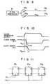
- one output signal from the clock generator 21 is supplied to two divided clock drivers 22 1 , 22 20
- These clock drivers 22 1 , 22 2 supply clock signals CL 1 , CL 2' respectively, to their corresponding clock signal lines 23 1 , 23 1 .
- the clock drivers 22 1 , 22 2 indicate different delay properties, depending on the load condition.
- Fig. 10 indicates the waveforms of the clock signals CL 1 , CL 2 .
- the characters tp l , tp 2 represent the length of time required for the clock signals CL 1 , CL 2 , respectively, to have their logic data converted from "1" to "0".
- a difference Atp between the two lengths of time denote a clock skew. This clock skew adversely affects the operation of the subject semiconductor integrated circuit device.
- Fig. 11 showing the operation of a shift register comprising a plurality of successively connected J-K flip-flop circuits.
- the flip-flop circuit 24 1 of the nth order is operated by the clock signal CL l of Fig. 10.
- the flip-flop circuit 24 2 of the n+lth order, and the flip-flop circuit 24 3 of the n+2th order are operated alike by the clock signal CL 2 of Fig. 10. If the length of time required for the negative edge trigger type flip-flop circuit of Fig.
- the object of this invention to provide a semiconductor integrated circuit device which comprises a plurality of divided clock drivers, and which has resolved the problem of the aforementioned clock skew.
- this invention provides a semiconductor integrated circuit device wherein one output signal from a clock generator is supplied to a plurality of clock signal lines, having one or more load circuits, through a plurality of divided clock drivers.
- the plural clock signal lines are connected together by a common connecting line.
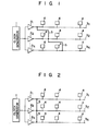
- Fig. 1 is an equivalent circuit of an LSI device according to one embodiment of this invention.
- This LSI device is formed on a semiconductor chip substrate (not shown) by the known manufacturing process.
- Reference numeral 1 denotes a clock generator.
- One output terminal of said clock generator 1 is connected to a plurality of clock drivers (2 1 , 2 2 , ... 2 N ). These clock drivers are properly distributed over the surface of the LSI chip substrate.
- Reference numerals 3 1 , ... 3N represent clock signal lines drawn out independently from the respective clock pulse driver output terminals.
- the clock signal lines 3 are connected to one or more load circuits 4, each of which has to be supplied with a clock signal.
- a common clock signal is supplied to all load circuits 4 through the independent clock signal lines 3 1 - 3 N .
- the clock signal lines 3 1 - 3 N are collectively connected by a common connecting line 5, said common connecting line 5 being metal wire in this embodiment. (For better understanding, said common connecting line 5 is shown in this and subsequent embodiments as a thick line.)
- the independent clock signal lines 3 1 - 3 N are connected together by the common connecting line 5, thus equalizing the load conditions of the plural clock drivers 2. Consequently, clock signals issue from the respective clock drivers 2 without delay, thereby substantially eliminating the occurrence of the clock skew. Since, as described above, the plural clock drivers 2 are properly distributed over the surface of the chip substrate, it is possible to resolve various problems which might arise from large local current variations, were only a single clock driver provided.
- the clock signal lines may be connected by a common connecting line at any point on said clock signal lines. If all the clock signal lines are connected together by the shortest common connecting line, no appreciable increase will result in the wire capacity. If the distributed clock drivers have a sufficient driving power in the aggregate, no consideration has to be given to any increase in the wiring capacity resulting from the provision of the common connecting line. Therefore, automatic placement and routing by computer can easily be applied.
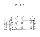
- Figs. 2 and 3 show the LSI devices embodying this invention, wherein the common connecting line for connecting the respective clock signal lines are set at different points from those indicated in Fig. 1.
- the common connecting line 5 is provided right near the output terminals of the clock drivers 2 1 - 2 N .
- the common connecting line 5 is set at a point furthest away from the respective clock drivers 2 1 - 2 N in a relationship entirely opposite to that of Fig. 2.
- the common connecting line 5 for connecting all the clock signal lines together need not be prepared from a metal, but may be formed of, for example, a polycrystalline silicon layer deposited on the chip substrate, or an impurity doped layer formed in the chip substrate.
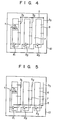
- Fig. 4 is a plan view of a CMOS gate array to which the semiconductor integrated circuit device of this invention is applied.
- a plurality of CMOS cell arrays 6 are mounted on the chip substrate 10. Interstices between the respective cell arrays 6 constitute wiring regions 7.
- a clock generator 1 is constituted by a plurality of CMOS cells involved in each cell array 6.
- Clock drivers 2 1 , 2 2 , 2 3 are constituted by one or more CMOS cells provided at one end of each cell array 6.
- First At wires extend in X direction parallel with the cell array 6.
- Second At wires extend in Y direction perpendicularly intersecting said Y direction.
- the clock signal lines 31, 3 2 , 3 3 extending from the corresponding clock drivers 2 1 , 2 2 , 2 3 are formed of the first At wire layer.
- a common connecting line 5 connecting the clock signal lines 3 1 , 3 2 , 3 3 together is prepared from a second Al layer and lies furthest from the clock drivers 2 1 , 2 2 , 2 3
- Figs. 5 to 7 indicate a CMOS gate array modified from the embodiment of Fig. 4.
- a common connecting line 5 connecting the clock signal lines 3 1 , 3 2t 3 3 together is prepared from a second Al wire layer and lies close to the output terminals of the clock drivers 2 1 , 2 2 , 2 3 .
- the clock driver 2 1 is set in the lowest position of a first cell array; the clock pulse driver 2 2 is positioned at the midpoint of a second cell array; and the clock pulse driver 2 3 lies in the uppermost position of a third cell array.
- a common connecting line connecting the clock signal lines 3 1 , 3 2 , 3 3 together is prepared from a second Al wire layer.
- a common connecting line connecting the clock signal lines 3 1 , 3 2 , 3 3 3 extends in both X and Y directions so as to substantially surround the region in which the cell arrays 6 are formed.
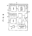
- Fig. 8 is a plan view of an LSI device, according to another embodiment of this invention, which is provided with a memory function.
- ROM read only memory
- RAM random access memory
- decoder decoder
- ALU arithmetic logic unit
- control circuit 15 A clock generator 1 which transmits a clock signal to said circuit elements is set in the corner of the chip substrate 10.
- Reference numerals 2 1 , 2 2 represent divided clock drivers.
- One clock driver 2 1 is intended to supply a clock signal to ROM 11, RAM 13 and decoder 12. This clock driver 2 1 has a relatively small drivability.
- the other clock driver 2 2 is intended to supply a clock signal to ALU 14 and control circuit 15, and has a greater drivability than the clock driver 2 1 .
- These clock drivers 2 1 , 2 2 are set in the vacant regions of the chip substrate 10.
- the clock signal line 3 1 drawn from the output terminal of the clock driver 2 1 , and the clock signal line 3 2 extending from the output terminal of the clock driver 2 2' are connected together by a common connecting line 5 formed in an elongated vacant area extending along part of the periphery of the chip substrate 10. Even the LSI device according to the embodiment of Fig. 8 can effectively eliminate the clock skew, thereby ensuring a reliable logic operation.
Landscapes
- Engineering & Computer Science (AREA)
- Theoretical Computer Science (AREA)
- Physics & Mathematics (AREA)
- General Engineering & Computer Science (AREA)
- General Physics & Mathematics (AREA)
- Nonlinear Science (AREA)
- Design And Manufacture Of Integrated Circuits (AREA)
- Semiconductor Integrated Circuits (AREA)
- Logic Circuits (AREA)
Applications Claiming Priority (2)
| Application Number | Priority Date | Filing Date | Title |
|---|---|---|---|
| JP204451/84 | 1984-09-29 | ||
| JP59204451A JPS6182525A (ja) | 1984-09-29 | 1984-09-29 | 半導体集積回路装置 |
Publications (3)
| Publication Number | Publication Date |
|---|---|
| EP0181059A2 true EP0181059A2 (fr) | 1986-05-14 |
| EP0181059A3 EP0181059A3 (en) | 1987-11-25 |
| EP0181059B1 EP0181059B1 (fr) | 1991-02-13 |
Family
ID=16490742
Family Applications (1)
| Application Number | Title | Priority Date | Filing Date |
|---|---|---|---|
| EP85305969A Expired - Lifetime EP0181059B1 (fr) | 1984-09-29 | 1985-08-22 | Circuit intégré à semi-conducteur pour la distribution de l'horloge |
Country Status (5)
| Country | Link |
|---|---|
| US (1) | US4661721A (fr) |
| EP (1) | EP0181059B1 (fr) |
| JP (1) | JPS6182525A (fr) |
| KR (1) | KR900000105B1 (fr) |
| DE (1) | DE3581754D1 (fr) |
Cited By (8)
| Publication number | Priority date | Publication date | Assignee | Title |
|---|---|---|---|---|
| EP0258975A3 (fr) * | 1986-07-09 | 1989-07-12 | Eta Systems, Inc. | Système de bus horloge pour circuit intégré |
| EP0335697A3 (en) * | 1988-03-29 | 1990-05-23 | Kabushiki Kaisha Toshiba | Integrated circuit device comprising interconnection wiring |
| EP0355769A3 (en) * | 1988-08-19 | 1990-06-06 | Kabushiki Kaisha Toshiba | Clock supply circuit clock supply circuit |
| EP0362691A3 (fr) * | 1988-10-05 | 1990-08-16 | Siemens Aktiengesellschaft | Dispositif de distribution d'horloge anti-déphasage |
| EP0418912A3 (en) * | 1989-09-22 | 1992-01-08 | Kabushiki Kaisha Toshiba | Semiconductor integrated circuit device |
| US5304826A (en) * | 1989-09-22 | 1994-04-19 | Kabushiki Kaisha Toshiba | Semiconductor integrated circuit device |
| DE4422456B4 (de) * | 1993-06-30 | 2004-07-01 | Intel Corporation, Santa Clara | Taktverteilungssystem für einen Mikroprozessor |
| DE4447848B4 (de) * | 1993-06-30 | 2005-10-27 | Intel Corporation, Santa Clara | Taktverteilungssystem für einen Mikroprozessor |
Families Citing this family (19)
| Publication number | Priority date | Publication date | Assignee | Title |
|---|---|---|---|---|
| ATE62774T1 (de) * | 1985-09-25 | 1991-05-15 | Siemens Ag | Netzwerk zur verarbeitung von daten grosser bitbreite mit einem sender und einer vielzahl von empfaengern. |
| JPS63238714A (ja) * | 1986-11-26 | 1988-10-04 | Hitachi Ltd | クロック供給システム |
| US5133064A (en) | 1987-04-27 | 1992-07-21 | Hitachi, Ltd. | Data processing system generating clock signal from an input clock, phase locked to the input clock and used for clocking logic devices |
| US5012427A (en) * | 1988-01-30 | 1991-04-30 | Kabushiki Kaisha Toshiba | Semiconductor integrated circuit and method of manufacturing the same |
| JPH02205908A (ja) * | 1989-02-03 | 1990-08-15 | Nec Corp | データ処理装置 |
| JPH0824143B2 (ja) * | 1989-02-08 | 1996-03-06 | 株式会社東芝 | 集積回路の配置配線方式 |
| JPH07101788B2 (ja) * | 1989-06-16 | 1995-11-01 | 富士通株式会社 | 電波放射抑制機能を有する二重化装置 |
| US5032743A (en) * | 1990-05-09 | 1991-07-16 | National Semiconductor Corporation | Skew clamp |
| US5396129A (en) * | 1992-05-25 | 1995-03-07 | Matsushita Electronics Corporation | Semiconductor integrated circuit apparatus comprising clock signal line formed in a ring shape |
| US5444407A (en) * | 1992-12-28 | 1995-08-22 | Advanced Micro Devices, Inc. | Microprocessor with distributed clock generators |
| US5438297A (en) * | 1992-12-30 | 1995-08-01 | Intel Corporation | Electrical trace having a closed loop configuration |
| JP3112784B2 (ja) * | 1993-09-24 | 2000-11-27 | 日本電気株式会社 | クロック信号分配回路 |
| US5570053A (en) * | 1994-09-26 | 1996-10-29 | Hitachi Micro Systems, Inc. | Method and apparatus for averaging clock skewing in clock distribution network |
| US5570054A (en) * | 1994-09-26 | 1996-10-29 | Hitachi Micro Systems, Inc. | Method and apparatus for adaptive clock deskewing |
| JPH10242396A (ja) * | 1997-03-03 | 1998-09-11 | Mitsubishi Electric Corp | クロックドライバ回路及び半導体集積回路装置 |
| KR100303533B1 (ko) * | 1998-03-30 | 2001-11-22 | 윤종용 | 전자렌지 |
| US6052012A (en) * | 1998-06-29 | 2000-04-18 | Cisco Technology, Inc. | Method and apparatus for clock uncertainly minimization |
| US6513149B1 (en) | 2000-03-31 | 2003-01-28 | International Business Machines Corporation | Routing balanced clock signals |
| DE102010048160A1 (de) * | 2010-10-11 | 2012-04-12 | Aaa Water Technologies Ag | Mehrstufige Membrandestillationsvorrichtung |
Family Cites Families (5)
| Publication number | Priority date | Publication date | Assignee | Title |
|---|---|---|---|---|
| US3104330A (en) * | 1960-02-11 | 1963-09-17 | Gen Electric | Clock pulse distribution system for synchronously driving a plurality of flip-flops |
| US3479603A (en) * | 1966-07-28 | 1969-11-18 | Bell Telephone Labor Inc | A plurality of sources connected in parallel to produce a timing pulse output while any source is operative |
| US3751591A (en) * | 1972-06-20 | 1973-08-07 | Ibm | Zero skew clock distribution system |
| JPS55136726A (en) * | 1979-04-11 | 1980-10-24 | Nec Corp | High voltage mos inverter and its drive method |
| US4504745A (en) * | 1982-06-14 | 1985-03-12 | Rockwell International Corporation | Clocked tri-state driver circuit |
-
1984
- 1984-09-29 JP JP59204451A patent/JPS6182525A/ja active Pending
-
1985
- 1985-06-12 KR KR1019850004137A patent/KR900000105B1/ko not_active Expired
- 1985-08-21 US US06/767,847 patent/US4661721A/en not_active Expired - Lifetime
- 1985-08-22 DE DE8585305969T patent/DE3581754D1/de not_active Expired - Lifetime
- 1985-08-22 EP EP85305969A patent/EP0181059B1/fr not_active Expired - Lifetime
Cited By (9)
| Publication number | Priority date | Publication date | Assignee | Title |
|---|---|---|---|---|
| EP0258975A3 (fr) * | 1986-07-09 | 1989-07-12 | Eta Systems, Inc. | Système de bus horloge pour circuit intégré |
| EP0335697A3 (en) * | 1988-03-29 | 1990-05-23 | Kabushiki Kaisha Toshiba | Integrated circuit device comprising interconnection wiring |
| EP0355769A3 (en) * | 1988-08-19 | 1990-06-06 | Kabushiki Kaisha Toshiba | Clock supply circuit clock supply circuit |
| US5013942A (en) * | 1988-08-19 | 1991-05-07 | Kabushiki Kaisha Toshiba | Clock supply circuit having adjustment capacitance |
| EP0362691A3 (fr) * | 1988-10-05 | 1990-08-16 | Siemens Aktiengesellschaft | Dispositif de distribution d'horloge anti-déphasage |
| EP0418912A3 (en) * | 1989-09-22 | 1992-01-08 | Kabushiki Kaisha Toshiba | Semiconductor integrated circuit device |
| US5304826A (en) * | 1989-09-22 | 1994-04-19 | Kabushiki Kaisha Toshiba | Semiconductor integrated circuit device |
| DE4422456B4 (de) * | 1993-06-30 | 2004-07-01 | Intel Corporation, Santa Clara | Taktverteilungssystem für einen Mikroprozessor |
| DE4447848B4 (de) * | 1993-06-30 | 2005-10-27 | Intel Corporation, Santa Clara | Taktverteilungssystem für einen Mikroprozessor |
Also Published As
| Publication number | Publication date |
|---|---|
| KR900000105B1 (ko) | 1990-01-19 |
| JPS6182525A (ja) | 1986-04-26 |
| DE3581754D1 (de) | 1991-03-21 |
| KR860002866A (ko) | 1986-04-30 |
| US4661721A (en) | 1987-04-28 |
| EP0181059B1 (fr) | 1991-02-13 |
| EP0181059A3 (en) | 1987-11-25 |
Similar Documents
| Publication | Publication Date | Title |
|---|---|---|
| US4661721A (en) | Clock driver distribution system in a semiconductor integrated circuit device | |
| US5045725A (en) | Integrated standard cell including clock lines | |
| EP1129486B1 (fr) | Cheminement de traces d'alimentation et de mise a la masse de circuit integre | |
| US4811073A (en) | Gate array arrangement | |
| EP0074825B2 (fr) | Production de circuits intégrés par des méthodes à tranche maîtresse | |
| JPS59172250A (ja) | 万能配列体 | |
| EP0612151B1 (fr) | Dispositif semi-conducteur capable de réduire un décalage d'horloge dans une pluralité de modèles de blocs de cablage | |
| US4947233A (en) | Semi-custom LSI having input/output cells | |
| JPS64821B2 (fr) | ||
| JPH01246845A (ja) | 集積回路 | |
| EP0021661B1 (fr) | Dispositif semiconducteur du type "masterslice" | |
| EP0416456B1 (fr) | Système d'alimentation pour circuit intégré du type prédiffusé | |
| JPH0571137B2 (fr) | ||
| US4746965A (en) | Integrated semiconductor circuit device | |
| EP0186769B1 (fr) | Structure de plaquette à circuit intégré avec compensation de charge capacitive du réseau d'interconnexions | |
| US5401988A (en) | Standard cell layout arrangement for an LSI circuit | |
| JPS61226943A (ja) | 自動配置配線用標準セル | |
| KR100329952B1 (ko) | 반도체 집적 회로 장치와 그 배선 배치 방법 | |
| US6855967B2 (en) | Utilization of MACRO power routing area for buffer insertion | |
| EP0278463B1 (fr) | Matrice de portes comportant un transistor enterré dans la région d'interconnexion | |
| JP2940045B2 (ja) | 半導体集積回路 | |
| JP2642377B2 (ja) | 半導体集積回路装置及びその製造方法 | |
| JP2889462B2 (ja) | 半導体集積回路 | |
| JPH01283846A (ja) | 半導体集積回路 | |
| JPH11261041A (ja) | 半導体集積回路装置およびその自動配線設計方法 |
Legal Events
| Date | Code | Title | Description |
|---|---|---|---|
| PUAI | Public reference made under article 153(3) epc to a published international application that has entered the european phase |
Free format text: ORIGINAL CODE: 0009012 |
|
| 17P | Request for examination filed |
Effective date: 19850909 |
|
| AK | Designated contracting states |
Kind code of ref document: A2 Designated state(s): DE FR GB |
|
| PUAL | Search report despatched |
Free format text: ORIGINAL CODE: 0009013 |
|
| AK | Designated contracting states |
Kind code of ref document: A3 Designated state(s): DE FR GB |
|
| 17Q | First examination report despatched |
Effective date: 19900404 |
|
| GRAA | (expected) grant |
Free format text: ORIGINAL CODE: 0009210 |
|
| AK | Designated contracting states |
Kind code of ref document: B1 Designated state(s): DE FR GB |
|
| REF | Corresponds to: |
Ref document number: 3581754 Country of ref document: DE Date of ref document: 19910321 |
|
| ET | Fr: translation filed | ||
| PLBI | Opposition filed |
Free format text: ORIGINAL CODE: 0009260 |
|
| 26 | Opposition filed |
Opponent name: TELEFUNKEN ELECTRONIC GMBH Effective date: 19911111 |
|
| PLAB | Opposition data, opponent's data or that of the opponent's representative modified |
Free format text: ORIGINAL CODE: 0009299OPPO |
|
| R26 | Opposition filed (corrected) |
Opponent name: TEMIC TELEFUNKEN MICROELECTRONIC GMBH Effective date: 19911111 |
|
| PGFP | Annual fee paid to national office [announced via postgrant information from national office to epo] |
Ref country code: FR Payment date: 19930805 Year of fee payment: 9 |
|
| PGFP | Annual fee paid to national office [announced via postgrant information from national office to epo] |
Ref country code: GB Payment date: 19930812 Year of fee payment: 9 |
|
| PGFP | Annual fee paid to national office [announced via postgrant information from national office to epo] |
Ref country code: DE Payment date: 19930823 Year of fee payment: 9 |
|
| RDAG | Patent revoked |
Free format text: ORIGINAL CODE: 0009271 |
|
| STAA | Information on the status of an ep patent application or granted ep patent |
Free format text: STATUS: PATENT REVOKED |
|
| 27W | Patent revoked |
Effective date: 19930715 |
|
| GBPR | Gb: patent revoked under art. 102 of the ep convention designating the uk as contracting state |
Free format text: 930715 |