EP0185534B1 - Ecran pour l'enregistrement d'une image obtenue par rayonnement - Google Patents
Ecran pour l'enregistrement d'une image obtenue par rayonnement Download PDFInfo
- Publication number
- EP0185534B1 EP0185534B1 EP19850309128 EP85309128A EP0185534B1 EP 0185534 B1 EP0185534 B1 EP 0185534B1 EP 19850309128 EP19850309128 EP 19850309128 EP 85309128 A EP85309128 A EP 85309128A EP 0185534 B1 EP0185534 B1 EP 0185534B1
- Authority
- EP
- European Patent Office
- Prior art keywords
- stimulable phosphor
- image storage
- radiation image
- fine
- layer
- Prior art date
- Legal status (The legal status is an assumption and is not a legal conclusion. Google has not performed a legal analysis and makes no representation as to the accuracy of the status listed.)
- Expired
Links
Images




Classifications
-
- G—PHYSICS
- G21—NUCLEAR PHYSICS; NUCLEAR ENGINEERING
- G21K—HANDLING OF PARTICLES OR IONISING RADIATION NOT OTHERWISE PROVIDED FOR; IRRADIATION DEVICES; GAMMA RAY OR X-RAY MICROSCOPES
- G21K4/00—Conversion screens for the conversion of the spatial distribution of X-rays or particle radiation into visible images, e.g. fluoroscopic screens
Definitions
- This invention relates to a radiation image storage panel comprising a stimulable phosphor, more particularly to a radiation image storage panel which provides a radiation image of high sharpness.
- a radiation image such as an X-ray image is frequently used for example in diagnosis of diseases.
- a radiation photograph is obtained by irradiating X-rays transmitted through a subject onto a phosphor layer (a fluorescent screen) to generate visible light; this visible light is then irradiated onto a film comprising a silver salt in a similar manner as in conventional photography. The film is then developed.
- a phosphor layer a fluorescent screen
- US-A-3,859,527 and JP-B-5512144 disclose a radiation image storage method employing visible light or IR-rays as the stimulating excitation light.
- This method employs a radiation image storage panel having a stimulable phosphor layer formed on a support. By irradiating the stimulable phosphor layer with radiation transmitted through a subject, a radiation image corresponding to the radiation transmission of the subject is produced.
- the stimulable phosphor layer is scanned with stimulating excitation light to radiate the accumulated radiation energy for the image, which is converted to light to provide an image according to the intensity of the light.
- the final image may be reproduced as a hard copy or reproduced on a CRT.
- the radiation image storage panel has high radiation absorption and light conversion (hereinafter referred to as "radiation sensitivity” as inclusive of both) as a matter of course, good image graininess and yet good sharpness.
- Radiation image storage panels having stimulable phosphor layers are generally made by applying and drying a dispersion containing 1 to 30 pm grains of a stimulable phopshor and an organic binder. Thus there is a low filling density of the stimulable phosphor (filling percentage 50%). Accordingly, in order to make the radiation sensitivity sufficiently high, it is necessary to use a thick phosphor layer as shown in Fig. 12(a) line (b).
- the stimulable phosphor is applied in an amount of 50 mg/cm 2 when the thickness of the stimulable phosphor layer is 200 pm.
- the radiation sensitivity increases linearly until saturated at a thickness of 450 pm or more because stimulated emission within the stimulable phosphor layer will not exit due to scattering between the phosphor grains if the layer is too thick.
- the image graininess is determined by the regional fluctuation in radiation quantum number (quantum mottle) or structural disturbance (structural mottle) of the stimulable phosphor layer
- the radiation quantum number may be reduced which increases quantum mottle or structural disturbance may occur which increases structural mottle. This lowers image quality.
- a thick stimulable phosphor layer is required.
- the radiation image storage panel of the prior art exhibits tendencies for radiation sensitivity and image graininess entirely opposite to that for image sharpness in relation to the thickness of the phosphor layer, and therefore there is a trade-off between radiation sensitivity, graininess and sharpness to some extent.
- Image sharpness in the radiation photographic method of the prior art is determined by expansion of the momentary emission (emission on irradiation of radiation) of the phosphor in the fluorescent screen, as is well known in the art.
- image sharpness in the method utilizing a stimulable phosphor as described above is not determined by the expansion of the stimulated emission of the stimulable phosphor in the radiation image storage panel, but rather is determined by the expansion of the stimulating excitation light within said panel.
- the stimulated emission by the stimulating excitation light irradiated at a certain time (ti) is desirably all collected and recorded as the output from the picture element (xi, yi) which is irradiated by the stimulating excitation light at that time. Therefore, if the stimulating excitation light is expanded, for example by scattering, within said panel and also excites the stimulable phosphor outside of the picture element (xi, yi), then output from a wider region than the picture element (xi, yi) is recorded as the output from that picture element.
- the emission stimulated by the stimulating excitation light irradiated at a time (ti) is only the emission from the picture element (xi, yi) on which the stimulating excitation light is truly irradiated at that time (ti), there is no influence on image sharpness even if the emission expands.
- a white powder may be mixed in the stimulable phosphor layer as disclosed in JP-B-55146447; and the radiation image storage panel may be coloured so that the average reflectance in the stimulating excitation wavelength region of the stimulable phosphor is less than the average reflectance in the stimulated emission wavelength region of the phosphor.
- these methods necessarily markedly lower the sensitivity if the sharpness is improved, and therefore cannot be said to be preferred methods.
- JP-B-59196365 a radiation image storage panel in which the stimulable phosphor layer contains no binder, which improves over the drawbacks of the prior art described above.
- the filling percentage of the stimulable phosphor is improved simultaneously with improvement of inclination of the stimulable excitation light and the stimulable emission, and radiation sensitivity and image graininess are improved simultaneously with improvement of image sharpness.
- the present invention seeks to provide a radiation image storage panel with improved radiation sensitivity and high image sharpness; and improved graininess and high image sharpness.
- the present invention provides a radiation image storage panel having a stimulable phosphor layer on a support, wherein said stimulable phosphor layer has a fine pillar-shaped block structure, the pillar-shaped blocks in said structure being abutted or separated from each other by gaps.
- the pillar-shaped blocks preferably extend perpendicularly to said support.
- Fig. 1 is a sectional view in the thickness direction of a radiation image storage panel (hereinafter sometimes referred to as "panel" when its meaning is distinct).
- 11 ij are each fine pillar-shaped blocks of the stimulable phosphor extending, preferably perpendicularly from the support and (11 ij) are gaps in the form of cracks, grooves or recesses.
- the stimulable phosphor layer 11 with a fine pillar-shaped block structure is formed from 11ij and (11ij).
- the blocks 11 ij preferably have a mean size of from 1 to 400 pm; the gaps may be of any size, provided that the blocks 11 ij are optically independent of each other, but are preferably from 0 to 20 pm on average.
- 13 is a protective layer which is preferably provided, and 14 is an adhesive layer which may optionally be provided to improve adhesion of the stimulable phosphor layer to the support 12.
- a reflection layer or absorption layer for stimulating excitation light and/or stimulated emission may be applied to the support surface.
- the pillar-shaped block structure may be of any desired pattern.
- Figs. 2(a), (b), (c) and (d) show examples of patterns.
- the thickness of the phosphor layer 11 in the panel of the present invention is preferably from 10 to 1000 pm, more preferably from 20 to 800 pm.
- a support having a homogeneous smooth surface or a support having a base pattern convenient for formation of a pillar-shaped block structure by attachment or deposition of a stimulable phosphor may be used.
- the mesh mask method may be used in which a metal mesh knitted with sufficiently fine metal wires (e.g. copper wires) or a perforated mesh densely perforated by means of a laser beam is pressure contacted on a support, and a stimulable phosphor is deposited by gas phase deposition, such as vacuum vapor deposition or sputtering to form pillar-shaped blocks;
- the moulding method may also be used in which a mould release agent, for example of the silicone type is applied as a surface coating for a mould having a convex pattern corresponding to the fine pillar-shaped block pattern, a stimulable phosphor is filled into the mould, a support is adhered onto the filled surface and the mould is removed to expose the pillar-shaped blocks.
- the crack method in which cracks are generated, for example by heat treatment, after uniform vapor deposition.
- a paint containing a stimulable phosphor suspended in a binder may be coated by means conventionally employed in printing methods, or pillar-shaped blocks may be grown according to the above gas phase deposition method.
- the support having a base pattern when intended to be coated by the above paint, can be obtained by forming a pattern corresponding to the fine pillar-shaped pattern based on the affinity of the paint for the support surface, similarly as in lithography printing.
- resist resins conventionally employed in photographic etching may also be used under the above conditions to provide a pattern on the support surface.
- the support may, for example, be a metal sheet having a metal oxide coat thereon.
- Techniques for formation of the metal oxide coat include coating the metal oxide on a metal surface conventionally used in these technical fields, such as a hard photomask or the preparation of transparent electroconductive films, for example, a chemical coating method, a spraying method or a CVD (Chemical Vapor Deposition) method, a RF ion plating method, a RF sputtering method or a vacuum deposition method.
- a chemical coating method such as a hard photomask or the preparation of transparent electroconductive films
- CVD Chemical Vapor Deposition
- the resist resin examples include posi-type and nega-type resist resins such as a photoresist, a vacuum UV-ray photoresist, an electron beam resist or an X-ray resist.
- the photoresist resins include those obtained by esterification of naphthoquinoneazide or benzoquinoneazide with novalac resins.
- the support is coated with the resist resin, a layer fractional pattern is printed and developed, and further etching is effected according to a wet or dry process to the depth at which the support surface is exposed, whereby a base layer 11 having a desired pattern comprising a texture of layer fractions 11 ij and gaps (11ij) is obtained.
- a layer fraction pattern can be easily prepared by sealing treatment and subsequent heat treatment of the porous aluminium oxide formed on the surface by anodic oxidation. This method is conventionally used in aluminium surface treatment.
- the anodic oxidation treatment of the aluminium support surface may be carried out, for example, on an aluminium plate having a thickness of about 0.5 mm, on the side where a stimulable phosphor is to be deposited, in a 8% oxalic acid solution, by passing a current of 1 A/cm 2 for about 2 hours, to form an anodically oxidized coating layer comprising porous aluminium oxide.
- the coating layer is washed with water and subsequently boiled in boiling water for about 1 hour.
- the porous aluminium oxide expands by incorporation of water of crystallization to form a coating layer comprising dense crystals. This operation is the so-called sealing treatment.
- heat treatment may be carried out at 250°C or higher, whereby the aluminium oxide loses the water of crystallization and shrinks to form a layer fraction pattern of fine island shapes surrounded and separated from each other by gaps formed by shrinkage.
- the aluminium oxide coating obtained preferably has a thickness of some micrometers or more.
- the layer fraction tend to become greater, it is necessary to select optimally the conditions for the anodic oxidation.
- the aluminium support may be one having impurity particles on the surface thereof.
- impurities in the support are precipitated and remain thereon without dissolving.
- impurities include Si, Fe and Cu, which are dot-like shaped with an average diameter of from 0.1 to 7 pm and black to brown in colour. Fine pillar-shaped blocks of a stimulable phosphor are formed on the surface of the support still containing impurities.
- aluminium supports generally contain, for example Si (25%), Fe (0.4%), Cu, Mn, Mg, Zn, V (each 0.05%) and Ti (0.03%), depending upon their purity.
- Fig. 14 is a sectional view in a thickness direction of a radiation image storage panel of this invention.
- the porous chromium layer known as porous chromium in plating technology, is a thin layer of chromium having many fine crevasses, which often have baggage-like shaped holes which are narrow at the opening thereof and broad at the bottom.
- the crevasses formed in the porous chromium layer are preferably present in a density of from 5000 to 50000 per cm 2.
- the depth of the crevasse d is preferably from 5 to 70% of the thickness of the porous chromium layer t; the porosity of the porous chromium layer is preferably from 10 to 45%.
- fine pillar-shaped blocks of a stimulable phosphor can be formed by vapor deposition.
- porous chromium layer and the stimulable phosphor layer may be an adhesive layer which assists the adhesion of the stimulable phosphor, or a reflective layer or an absorption layer for stimulable excitation light and/or stimulable emission, if desired.
- the support having a base pattern may be prepared according to the method in which ink silk or gravure printed, preferably with burning, to form a base pattern corresponding to the fine pillar-shaped pattern; the method in which a base pattern suitable for gas phase deposition of a stimulable phosphor physically and/or chemically is prepared by photographic etching; or the method in which a base pattern is prepared by application of a sealing treatment and heat treatment to an aluminium plate subjected to anodic oxidation.
- a base pattern in the form of fine partitioned island regions physically and/or chemically suitable for gas phase deposition is obtained, said regions being surrounded by fine streaks, grooves, convexities or cracks, in which gas phase deposition can proceed with difficulty.
- a thin pattern layer of a stimulable phosphor may be formed on the support and gas phase deposition may subsequently be applied to the base pattern.
- the radiation image storage panel of the present invention preferably comprises a support having on its surface a large number of fine concavo-convex patterns, which may be produced, for example, by the above method, and a stimulable phosphor layer comprising a fine pillar-shaped block structure having the above surface structure, provided thereon.
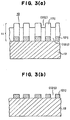
- Fig. 3(a) is a sectional view of a radiation image storage panel of the present invention.
- Fig. 3(b) is a sectional view in the thickness direction of a support having a concavo-convex pattern before provision of the stimulable phosphor layer having the above fine pillar-shaped block structure.
- the distributed pattern on the above support may be any desired pattern, such as shown in Figs. 2(a), 2(b), 2(c) or 2(d).
- Fig. 3(a) 10 is a panel
- 12ij are convexities and (12ij) concavities of the support 12 is a support
- 11 ij are each fine pillar-shaped blocks of stimulable phosphor having the above convexities
- (11 ij) are each pillar-shaped block having the above concavities (12ij).
- the stimulable phosphor layer 11 is formed from 11ij and (11ij).
- the convexities 12ij and concavities (12ij) preferably have a mean size of from 10 to 400 pm, more preferably from 15 to 100 pm.
- the concavo-convex surface of the support may be provided with an adhesive layer to aid adhesion of the stimulable phosphor layer or a reflection layer or an absorption layer for stimulating excitation light and/or stimulated emission.
- the boundary between the blocks (11ij) grown on the concavity (12ij) and the blocks 11ij grown on the convexity 12ij is discontinuous, so that the blocks (11ij) and the blocks 11 are optically independent.
- stimulating excitation light enters the stimulable phosphor layer having fine pillar-shaped block structures independent of each other, it reaches the bottom of the pillar-shaped block with repeated reflections against the inner surface of the block due to the optical induction effect of the fine pillar-shaped block structure without exiting the block, where it is absorbed or reflected, and again emits in the pillar direction while reflecting against the inner surface of the block.
- image sharpness is markedly increased while the chances of stimulating excitation are also increased.
- the radiation image storage panel of Fig. 3 has support having a surface structure in which a large number of fine tiles are separated from each other by fine gaps, and a stimulable phosphor comprising a fine pillar-shaped block structure having the above surface structure is provided thereon.
- the surface of the support has a structure in which a large number of fine tiles with sizes of from 1 to 400 ⁇ m separated from each other by gaps in the form of cracks, grooves or recesses with widths of from 0.01 to 20 Il m, and the stimulable phosphor layer is formed on the above fine tiles, thus providing fine pillar-shaped blocks separated from each other with the above gaps being reproduced as indentations in the surface of the block structure.
- the stimulating excitation light entering the stimulable phosphor layer progresses only perpendicularly to the support with total reflection through the fine pillar-shaped block with substantially no dissipation laterally. Since the gaps on the support surface remain as such, the fine pillar-shaped blocks forming the stimulable phosphor layer are optically completely independent so that lateral dissipation of the stimulating excitation light is very low.
- gas phase deposition such as vacuum vapor deposition or sputtering is preferred from the viewpoint of sensitivity and the technical aspect for formation of pillar-shaped blocks.
- an anodically oxidized aluminium plate subjected to sealing treatment and subsequently to heat treatment is preferred, and the production method using said support is useful.
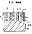
- Fig. 5(a) is a sectional view in the thickness direction of a radiation image storage panel of an embodiment of the present invention.
- Fig. 5(b) is a sectional view of a support having a surface structure in which the fine tiles are separated from each other by fine gaps before provision of the stimulable phosphor layer having the fine pillar-shaped block structure.
- the pattern of the fine tiles on the support may be any desired.
- examples of distributed patterns are shown as (a), (b), (c) and (d).
- 10 is a panel of the present invention
- 12ij are each fine tiles on the support surface and (12ij) are gaps in the form of cracks, grooves or recesses surrounding said fine tiles.
- 12' is a layer of fine tiles dispersed as islands on the support surface formed of 12ij and (12ij).
- 12 is a support.
- 11 are each fine pillar-shaped blocks of stimulable phosphor deposited by gas phase deposition on the fine tiles, and (11ij) are deep gaps between the 11 selectively deposited on 12ij.
- 14 is an optional adhesive layer and 13 is a protective layer which is preferably provided.
- the stimulable phosphor layer 11 comprising a fine pillar-shaped block structure is formed from 11 ij and (11ij).
- the gaps (11 ij) as herein mentioned include mere cracks with substantially no gap only formed on the phosphor layer surface, and therefore a fine multipyramid block structure is included within the scope of the fine pillar-shaped block structure.
- a perspective view of an aluminium support subjected to anodic oxidation treatment, sealing treatment and heat treatment is shown in Fig. 6.
- the adhesive layer 14 On the fine tiles 12ij, the adhesive layer 14, and a reflection layer or absorption layer for stimulated emission and/or stimulating excitation light may be similarly provided to give a multi-layer structure.
- the radiation image storage panel has a large number of fine tiles on a support surface, a net with five strings surrounding said fine tiles separating them from each other, and a stimulable phosphor layer with a block structure extending perpendicularly to the layer of fine tiles.
- Fig. 7(a) is a sectional view in the thickness direction of a radiation image storage panel of the present invention.
- Fig. 7(b) is a sectional view of the support bearing fine tiles and a net with five strings surrounding and separating said fine tiles provided thereon before provision of the stimulable phosphor layer having a fine pillar-shaped block structure
- Fig. 7(c) is a sectional view of the support bearing only the fine tiles without the net.
- 10 is a panel of the present invention
- 12ij are fine tiles each having a thickness d
- (12ij) are gaps in the form of cracks, grooves or recesses surrounding the fine tiles.
- 15ij are fine strings of a net with a height h which fill the (12ij) and separate respective 12ij from each other. h is preferably not smaller than d.
- the stimulable phosphor layer 11 having a fine pillar-shaped block structure according to the present invention is formed from 11 ij and (11 ij).
- 13 is a protective layer which is preferably provided, and 12 is a support.
- the gap (11ij) as herein mentioned includes a crack with no substantial gap, and therefore the fine pillar-shaped block structure includes within its scope a fine multipyramid block structure.
- the radiation image storage panel may be provided with a stimulable phosphor comprising a fine pillar-shaped block structure having crevasses developed from the gap between the fine tiles towards the layer surface by applying a shock treatment to the stimulable phosphor layer deposited perpendicularly to the surfaces of the fine tiles: It is preferred that heat treatment is combined with the shock treatment.
- Fig. 8(a) is a sectional view of a radiation image storage panel in the thickness direction.
- Fig. 8(b) is a sectional view in the thickness direction of a panel when the above stimulable phosphor layer is deposited before shock treatment, and
- Fig. 8(c) is a sectional view of a previous state in which the support bears only fine tiles without the stimulable phosphor layer.
- the fine tiles may be distributed on the support in any desired pattern.
- Fig. 8(a) 10 is a panel of the present invention
- 12ij are each fine tiles on the support surface
- (12ij) are gaps, for example in the form of cracks, grooves or recesses, surrounding the fine tiles.
- 12' is a pattern layer of fine tiles scattered in islands on the support surface, made of the above 12ij and (12ij).
- (11ij) is a cavity within the deposition layer, which is formed during deposition of the stimulable phosphor on the distributed pattern layer 11 by first depositing the stimulable phosphor on the fine tiles 12ij and gradually expanding the deposition area until at last effecting bonding of the deposited layer; this cavity may be very small or may reach the surface to become a crevasse depending on the size of the gaps (12ij).
- 11 is a stimulable phosphor deposition layer including the above mentioned cavity or crevasse (11 ij).
- 11ij are each fine pillar-shaped blocks having the stimulable phosphors deposited on the fine tiles isolated from each other by shock treatment on the deposited layer 11 to develop each cavity (11 ij) to the surface of the deposited layer to form a crevasse.
- (11 ij) are crevasses between the fine pillar-shaped blocks 11 ij.
- the stimulable phosphor layer 11 having a fine pillar-shaped block structure is formed from 11 ij and (11ij).
- 12 is a support and 13 is a protective layer which is preferably provided.
- a crevasse developed from the surface of the layer may be provided.
- the crevasse after formation of the stimulable phosphor layer by means of, for example, various vapor deposition methods, the crevasse may be formed by providing a thermal shock. That is, the crevasse can be formed by heating and cooling utilizing the thermal expansion difference between the stimulable phosphor and the support.
- a panel with a stimulable phosphor deposited thereon is heated to about 300°C in an inert gas such as nitrogen, and after reaching thermal equilibrium with the original panel, crevasses are formed in the stimulable phosphor layer when the panel is cooled by introducing a large amount of cooled nitrogen.
- an inert gas such as nitrogen
- crevasses are formed by strain due to the difference between the surface temperature of the stimulable phosphor layer and the temperature of the support based on the specific heats thereof-or speeds of cooling, almost all of crevasses occur from the surface of the stimulable phosphor layer to provide a structure as shown in Fig. 14. Further heating may be carried out for the support side and cooling on the phoshor side.
- the heating temperature may be lower, for example about 150°C when an alcohol is employed for cooling.
- the above method for forming crevasses may be interposed during vapor deposition of the stimulable phosphor layer.
- the method for forming crevasses is not limited to thermal treatment; any method may be employed so long as it can provide crevasses without imparting the function of the panel.
- a method may be employed in which, during the latter half of formation of the stimulable phosphor layer by vapor deposition, crevasses are formed by increasing a concentration of an inert gas such as argon to form gaps in the phosphor layer and providing a thermal shock from the layer surface side.
- Crevasses can also be formed, for example, by providing an ultrasonic or electrical shock to a crystalline dislocation line directed to the layer surface, which is formed during deposition.
- a stimulable phosphor layer may be formed on a protective layer which protects the panel surface by vapor deposition, and then crevasses can be introduced by a panel producing method to be adhered to the support after deposition.
- a stimulable phosphor layer can be formed by any vapor deposition method. Then, since the stimulable phosphor starts to deposit on the surface of the above protective layer film as fine prismatic crystals, gaps between these prismatic crystals form as stimulable phosphor layer crevasses extended in a direction almost perpendicular to said film surface. Thus crevasses open to the surface can be introduced by adhering them to the support.
- the above crevasses may be grown by a shock treatment such as a thermal treatment.
- the thus obtained fine pillar-shaped blocks become finer-sized pillar-shaped blocks.
- the radiation image storage panel of the present invention may have at least one pillar-shaped stimulable phosphor on the upper part of at least one fine grain layer on the support.
- Figs. 9(a) and 9(b) are sectional views in the thickness direction of a radiation image storage panel of the above embodiment.
- 11ij are each fine pillar-shaped blocks extending perpendicularly from the support surface, (11 ij) are each gaps between 1 ij in the form of cracks, grooves or recesses.
- the stimulable phosphor layer 11 having a fine pillar-shaped block structure is formed from 11ij and (11ij).
- 11a a is a layer comprising grains with a thickness of 1/2 or less of the entire film thickness, preferably 1/10 or less; the grains may be spread in at least one layer.
- the grains may have a mean grain size of 50 pm or less, preferably 15 pm or less.
- the layer 11 a can be obtained by gas phase deposition such as vacuum deposition or sputtering.
- various metals such as ZnO, Ti0 2 or A1 2 0 3 , metal sulfides such as ZnS, amorphous silicon, compounds such as SiC, SiN or Si0 2 , or alkali halide crystals and stimulable phosphors as hereinafter described may be used.
- metals metal oxides such as ZnO, Ti0 2 or A1 2 0 3 , metal sulfides such as ZnS, amorphous silicon, compounds such as SiC, SiN or Si0 2 , or alkali halide crystals and stimulable phosphors as hereinafter described may be used.
- alkali halide crystals are preferred to obtain a fine pillar-shaped pillar structure 11 ij.
- the layer 11a shown in Fig. 10 may be obtained by, for example, vapor deposition of, for example, alkali halide crystals in a vacuum of about 10- 3 Torr (0.133 Pa).
- fine pillar-shaped blocks 11ij can be grown on the grains by gas phase deposition.
- the layer 11 a also enhances adhesion to 11ij.
- the above layer constituting operation may be repeated for the necessary number of times.
- the radiation image storage panel of the present invention may also have a stimulable phosphor layer with at least two layers of a pillar-shaped block structure.
- Fig. 11 is a sectional view in the thickness direction of a radiation image storage panel of the above embodiment, in which 11 is the recording layer of the panel and 12 is a support.
- the base layer 12' is a base layer having a thickness of 1/2 or less, preferably 1/10 or less of the film thickness of the recording layer 11, said base layer 12' comprising layer fractions 12ij dispersed in islands as exemplified in Fig. 10 and gaps (12ij) shaped in concavities or cracks therearound separating the islands from each other.
- 11 is a stimulable phosphor layer on the above base layer 12'. It comprises at least two layers of pillar-shaped blocks 11ij and the gaps (11 ij) formed corresponding to the above gaps (12ij).
- pillar-shaped blocks 11Aij and 11Bij comprising stimulable phosphors A and B.
- the mean size of 11ij ij is preferably from 1 to 400 pm.
- the bonded portion may have a function such a a filter.
- the stimulable phosphors A and B may be either the same or different.
- the stage number of the block lamination is not limited, and it is possible to make a continuous constitution (infinite stage number), in which a certain characteristic of the stimulable phosphor, for example, optical reflectance, is continuously changed.
- (11ij) are crevasses or boundaries between the pillar-shaped blocks 11ij corresponding to the gaps (12ij) as described above, which are provided to make respective 11 ij blocks optically independent of each other.
- the width of (11 ij) is preferably from 0 to 20 ⁇ m.
- (11 ij) are named comprehensively as crevasses.
- 13 is a protective layer and 14 is an adhesive layer between the base layer 12' and the stimulable phosphor layer 11. These layers are provided if necessary.
- the stimulable phosphor in the radiation image storage panel of the present invention refers to a phosphor exhibiting stimulated emission corresponding to the dose of the first light or high energy radiation by optical, thermal, mechanical or electrical stimulation (stimulating excitation) after irradiation by the first light or high energy radiation. It is preferably a phosphor exhibiting stimulated emission by a stimulating excitation light of a wavelength of 500 nm or longer.
- Examples of stimulable phosphor are: BaS0 4 :Ax (where A is at least one of Dy, Tb and Tm, and 0.001 ⁇ x ⁇ 1 mol %) disclosed in JP-B-4880487; MgS0 4 :Ax (where A is either Ho or Dy and 0.001 ⁇ x ⁇ 1 mole %) disclosed in JP-B-4880488; SrSO 4 :Ax (where A is at least one of Dy, Tb and Tm and 0.001 ⁇ x ⁇ 1 mole %) disclosed in JP-B-4880489; those in which at least one of Mn, Dy and Tb is added to, for example, Na 2 S0 4 , CaS0 4 and BaS0 4 as disclosed in JP-B-51298891976; those such as BeO, Lif, MgS0 4 and CaF 2 as disclosed in Japanese Provisional Patent Publication No.
- JP-B-5230487 those such as Li 2 B 4 0 7 ,Cu,Ag as disclosed in JP-B-5339277; those such as Li 2 O ⁇ (B 2 O 2 )x:Cu where 2 ⁇ x ⁇ 3) and Li 2 O ⁇ (B 2 O 2 )x:Cu,Ag (where 2 ⁇ x ⁇ 3), as disclosed in JP-B-5447883; SrS:Ce,Sm, SrS:Eu,Sm, La 2 0 2 S:Eu,Sm and (Zn,Cd)S:Mn,X (where X is a halogen) disclosed in US-A-3,859,527; ZnS:Cu,Pb phosphors disclosed in JP-B-5512142; and barium aluminate phosphors BaO ⁇ xAl 2 O 3 :Eu (where 0.8 ⁇ x ⁇ 10) and alkaline earth metallosilicate type phosphors M"O ⁇ xSi0 2 :A (where M
- phosphors include, as disclosed in JP-B-5512143, those of the formula: (where X is at least one of Br and CI and 0 ⁇ x+y ⁇ 0.6, xy ⁇ 0 and 10 -6 ⁇ e ⁇ 10 -2 ); those disclosed in JP-B-5512144 which corresponds to US-A-4,236,078: (where Ln represents at least one of La, Y, Gd and Lu; X represents CI and/or Br; A represents Ce and/or Tb; and 0 ⁇ x ⁇ 0.1); those disclosed in JP-B-5512145: (where M" represents at least one of Mg, Ca, Sr, Zn and Cd; X represents at least one of Cl, Br and I; A represents at least one of Eu, Tb, Ce, Tm, Dy, Pr, Ho, Nd, Yb and Er; and O ⁇ x ⁇ 0.6 and 0 ⁇ y ⁇ 0.2); those discdlosed in JP-B-5584389: (where X is at least one of Cl, Br, Br
- Alkalide halide phosphors are preferred, because stimulable phosphor layers can be formed easily by methods such as vacuum vapor deposition and sputtering.
- the stimulable phosphor is not limited to those described above; any phosphor which can exhibit stimulated fluorescence when irradiated with a stimulating excitation light after irradiation by radiation may be used.
- the radiation image storage panel of the present invention may have a group of stimulable phosphor layers comprising one or more stimulable phosphor layers comprising at least one of the stimulable phosphors as mentioned above.
- the stimulable phosphors contained in respective stimulable phosphor layers may be identical or different.
- Various polymeric materials, glasses or metals may, for example, be used as the support.
- Materials which can be worked into flexible sheets or webs are preferred for information recording materials, such as plastics films such as cellulose acetate film, polyester film, polyethyleneterephthalate film, polyamide film, polyimide film, triacetate film or polycarbonate film, metal sheets, for example of aluminium, iron, copper or chromium or metal sheets having coats of the oxides of said metals.
- These supports may have thicknesses which differ depending on the material of the support.
- the thicknesses are generally from 80 ⁇ m to 1000 pm, more preferably from 80 pm to 500 pm from the standpoint of suitability of handling.
- a protective layer to protect physically and chemically the exposed surface of the stimulable phosphor layers.
- the protective layer may be formed by direct coating of a coating liquid on the stimulable phosphor layer, or alternatively a protective layer separately formed may be adhered to the stimulable phosphor layer.
- the materials for the protective layer include, for example, conventional materials such as cellulose acetate, nitrocellulose, polymethyl methacrylate, polyvinyl butyral, polycarbonate, polyester, polyethyleneterephthalate, polyethylene, polyvinylidene chloride and nylon (trade name).
- the protective layer may also be formed by laminating inorganic substances such as SiC, Si0 2 , SiN or A1 2 0 3 by, for example, vacuum deposition or sputtering.
- These protective layers preferably have a thickness of from 0.1 pm to 100 pm.
- the first method is vacuum deposition.
- a support is first set in a vacuum deposition device and the device is evacuated to about 10- 6 Torr (0.133x10 -3 Pa).
- At least one of the stimulable phosphors is evaporated by heating by, for example resistance heating or electron beams, to deposit the stimulable phosphor on the support surface.
- a stimulable phosphor layer containing no binder is formed. It is also possible to form the stimulable phosphor in a plurality of separate stages in the vapor deposition step. A plurality of resistance heaters or electron beams may be employed to effect co-deposition.
- a protective layer is preferably provided on the side opposite to the support side of the stimulable phosphor layer.
- the above vacuum vapor deposition method it is also possible to form a stimulable phosphor layer simultaneously with synthesis of the desired phosphor layer on a support by co-depositing stimulable phosphor starting materials by means of a plurality of resistance heaters or electron beams.
- the subject on which vapor deposition is effected (the support or protective layer) may be cooled or heated, if desired. After completion of vapor deposition, the stimulable phosphor layer may be subjected to heat treatment.
- the second method is a sputtering method.
- the device is internally evacuated to a vacuum degree of about 10- s Torr (0.133x10- 3 Pa), and then an inert gas such as Ar or He is introduced to adjust the pressure to about 10- 3 Torr (0.133 Pa).
- sputtering is effected to deposit the stimulable phosphor on the support surface to a desired thickness.
- the stimulable phosphor layer can be formed in a plurality of separate stages, similarly as in the vacuum vapor deposition method, or alternatively the stimulable phosphor layer can be formed using a plurality of targets comprising stimulable phosphors different from each other by sputtering at the same time or successively.
- a protective layer may be formed, if desired, on the side opposite to the support side of the stimulable phosphor layer.
- the sputter method it is also possible to use a plurality of starting materials for the stimulable phosphor as the targets, sputtering these at the same time or successively to form a stimulable phosphor layer simultaneously with synthesis of the stimulable phosphor.
- reactive sputtering may be conducted by introducing a gas such as O2 or H 2 if necessary.
- the subject to be sputtered (the support or protective layer) may be either cooled or heated.
- the stimulable phosphor layer may be subjected to heat treatment after completion of sputtering.
- the third method is a CVD method.
- An organometallic compound containing the desired stimulable phopshor or starting materials therefor is decomposed by, for example, heat or high frequency power to obtain a stimulable phosphor layer containing no binder.
- the gas phase deposition method is most preferred in view of the certainty of pillar-shaped block formation and sensitivity.
- steps (c) and (a) are conducted in the same manner as steps (b) and (a) respectively in Fig. 5 as described above.
- the material for the net with fine strings 15ij surrounding the fine tiles 12ij and filling the gaps (12ij) is preferably one having different crystallization conditions and/or physical properties such as thermal expansion. It is practically a metal.
- the net may be prepared by electric plating.
- an electroconductive layer such as a metal or indium oxide is provided on its surface by vacuum vapor deposition or other methods before step (c), and said electroconductive layer is exposed by etching.
- a metal sheet having a metal oxide coating layer is used.
- a net with fine strings 15ij comprising, for example, nickel or chromium is formed.
- the stimulable phosphor as fine pillar-shaped blocks on the fine tiles 12ij in this case, it is preferable that the height h of the fine strings 15ij of the net is, equal to or greater than the thickness d of the fine tiles on the electroconductive support surface.
- Fig. 8(c) The step of Fig. 8(c) is conducted in the same manner as the successive combinations of Fig. 5(b) and Fig. 7(b) and the step of Fig. 8(b) in the same manner as the step of Fig. 3(a).
- the shock treatment imparts a fine pillar-shaped (including polypyramid-shaped) block structure having an inner reflective surface against the stimulating excitation light incident on the stimulable phosphor layer deposited on the fine tiles 12ij having formed crevasses or cracks formed on the surface by giving shock to the deposited layer with the acting base point, thereby propagating ruptures up to the surface.
- any method may be employed, provided that ruptures in the form of crevasses or cracks can be provided without impairing the function of the panel.
- a heat treatment method may be employed in which ruptures are formed by heating or cooling using the difference in thermal expansion between the stimulable phosphor and the plastic, metal of the support or net as described above; a sonication method in which the crystal dislocation line or the structural distortion existing at the bonded point of the phosphor in the cavityi (11 ij) is vibrated to permit the cracks to grow and develop on the surface from the bonded point; or a voltage rupture method, for example simulating insulating destruction of a capacitor with an alternating current.
- the stimulable phosphor layer 11 having a fine pillar-shaped block structure preferably has effective inner reflective surfaces against stimulating excitation light in each block and a substantially continuous and smooth surface to enhance of sensitivity and sharpness, the rupture on the surface should preferably be a crack with no substantial gap.
- the heat treatment method may conveniently be used.
- the heat treatment method may be carried out by heating the panel completed in step (b) to about 300°C in an inert gas such as nitrogen and cooling the panel after it has reached thermal equilibrium with a large amount of cold nitrogen gas, to develop the crack from the tip of the cavity (11 ij) (bonded point of the phosphor) until it reaches the surface.
- the heating temperature may be lower.
- a temperature of about 150°C can be used when cold alcohol is used for cooling.
- the above gas phase vapor deposition method may be employed.
- the pressure in the device may be made to about 10-' Torr (1.33x10- 5 Pa) similarly as described above and, after treatment of the support, the vacuum degree is controlled to about 4x10-' Torr (0.532 Pa) with argon.
- a stimulable phosphor layer containing no binder is formed; it is also possible to effect co-deposition by use of a plurality of resistance heaters or electron beams in the vapor deposition step.
- the radiation image storage panel After completion of vapor deposition, the radiation image storage panel can be produced following prescribed procedures.
- sputtering is effected with the use of, for example, an alkali halide crystal Rbl as the target. Sputtering is stopped when a pattern as shown in Fig. 10 is formed. Using, for example, rubidium bromide activated with thallium as the target, sputtering is further effected on the layer 11a to deposit a stimulable phosphor with a fine pillar-shaped block structure to a desired thickness.
- a stimulable phosphor with a fine pillar-shaped block structure may be deposited to a desired thickness by vacuum vapor deposition.
- the layer can be provided thinly and uniformly, and also that deposition of the stimulable phosphor with a fine pillar-shaped block structure can be done rapidly.
- the panel of the present invention having at least two layers of pillar-shaped blocks as shown in Fig. 11, either one of the gas phase deposition methods or a successive combination of both may be used.
- the stimulable phosphor with a pillar-shaped block structure can have a variety of optical, electromagnetic or other physical characteristics such as strength, various controlling mechanisms and composite functions can be introduced into the panel.
- the light-receiving efficiency of stimulating excitation light incident obliquely on the panel can be improved.
- durability of the panel can be improved.
- the humidity resistance of the panel can be improved to enhance storability.
- Fig. 12(a) shows one example (line (a)) of the relationship of the thickness of the stimulable phosphor layer in the radiation image storage panel of the present invention obtained by gas phase deposition and the amount of the stimulable phosphor corresponding to said layer thickness versus the radiation sensitivity.
- the stimulable phosphor layer formed by gas phase deposition as used in the present invention contains no binder, and therefore the amount of the stimulable phosphor applied (filling ratio) is about twice that provided by coating in the prior art.
- the amount of the stimulable phosphor applied is about twice that provided by coating in the prior art.
- the stimulable phosphor layer produced by gas phase vapor deposition has excellent transparency and is highly transmissive of stimulating excitation light and stimulated emission. Therefore the layer can be made thicker than the stimulable phosphor layer of the prior art to further increase radiation sensitivity.
- the stimulating excitation light repeats reflection on the inner surface of the blocks with little dissipation out of the block, and therefore image sharpness is improved. Lowering of sharpness accompanied with an increase in thickness of the stimulable phosphor layer can be reduced.
- the radiation image storage panel of the present invention can given excellent sharpness, graininess and sensitivity when employed in the radiation image storage method schematically shown in Fig. 13.
- 41 is a radiation generating device
- 42 is a subject
- 43 is a radiation image storage panel of the present invention
- 44 is a stimulating excitation light source
- 45 is a photoelectric converting device for detection of the stimulated emission radiated from said radiation image storage panel
- 48 is a filter for separating the stimulating excitation light from stimulated emission to permit only the stimulated emission to pass.
- the devices of 45 et seq are not particularly limited to those as mentioned above, provided that they can reproduce the optical information from 43 as an image in some form.
- radiation from the radiation generating device 41 passes through the subject 42 and enters the radiation image storage panel 43 of the present invention.
- the incident radiation is absorbed by the stimulable phosphor layer of the radiation image storage panel 43 to form an image corresponding to the radiation transmitted image.
- the accumulated image is excited by stimulating excitation light from the stimulating excitation light source 44 and stimulated emission is released.
- the stimulable phosphor layer since the stimulable phosphor layer has a fine pillar-shaped block structure, the diffusion of the stimulating excitation light within the stimulable phosphor layer during scanning by the above stimulating excitation light is inhibited.
- the intensity of the stimulated emission radiated is proportional to the radiation energy quantity accumulated, and the optical signal can be converted photoelectrically by means of, for example, a photoelectric converting device 43, such as a photomultiplier tube, and reproduced by an image reproducing device 46 as an image, whereby the image of the subject can be observed.
- a photoelectric converting device 43 such as a photomultiplier tube
- a 500 pm thick aluminium sheet support was set in a depositing vessel.
- an alkali halide stimulable phosphor (0.9 RbBr - 0.1CsF:0.01 TI) was placed in a tungsten boat and set on electrodes for resistance heating and subsequently the deposition vessel was evacuated to a vacuum degree of 2x10- 6 Torr (0.266x10⁻³ Pa).
- sensitivity to X-rays is shown as a relative value to that of the panel A, which is 100.
- the modulation transmission function (MTF) is the value at 2 cycles mm space frequency, and graininess is represented by 0, 0 or X meaning good, common or bad respectively.
- a mesh of 50 pm diameter metal wire was pressure coated, and the composite was set in a sputtering device.
- an alkali halide stimulable phosphor (0.95 RbBr - 0.05 CsF:0.005 TI) was set in the sputtering device, followed by evacuation to a vacuum degree of 1x10 -6 Torr (0.133x10 -3 Pa).
- Sputtering was performed with Ar as the sputter gas to effect deposition until the thickness of the layer on the metal mesh was 300 pm to obtain a radiation image storage panel B of the present invention.
- the panel B was evaluated similarly as in Example 1 to obtain the results in Table 1.
- a 500 pm thick aluminium plate was coated with a photoresist resin and subjected to pattern exposure and development to form a minute concavo-convex pattern as shown in Fig. 2(d) to provide a support.
- the minute concavo-convex pattern had a size of 80 umx80 ⁇ m and a thickness of 40 um.
- the support was set in a vapor deposition vessel, an alkali halide stimulable phosphor (0.9 RbBr . 0.1 CsF:0.01 TI) was placed in a tungsten boat and set on electrodes for resistance heating and subsequently the deposition vessel was evacuated to a vacuum degree of 2x10- 6 Torr (0.266x10- 3 Pa).
- an alkali halide stimulable phosphor 9 RbBr . 0.1 CsF:0.01 TI
- sensitivity to X-rays is shown as a relative value to that of the radiation image storage panel C, which is 100.
- the modulation transmission function (MTF) and graininess are shown as in Table 1.
- a radiation image storage panel D of the present invention was prepared in the same manner as in Example 3, except for using as the support a black polyethyleneterephthalate film, the surface of which was subjected to embossing to form a fine concavo-convex pattern.
- the panel D was evaluated similarly as in Example 3 to give the results shown in Table 2.
- an alkali halide stimulable phosphor (0.9 RbBr . 0.1 CsF:0.01 TI)
- one part by weight of a polyvinyl butyral resin and five parts by weight of a solvent (cyclohexanone) were mixed and dispersed to prepare a stimulable phosphor coating liquid.
- the coating liquid was applied uniformly on a black polyethylene terephthalate film as a support placed horizontally with a thickness of 300 ⁇ m, followed by natural drying, to obtain a 300 pm thick stimulable phosphor layer.
- the comparative radiation image storage panel a thus obtained was evaluated similarly as in Example 3 to obtain the results listed in Table 2.
- a radiation image storage panel e was prepared in the same manner as in Comparative Example 1 except for making the thickness of the stimulable phosphor layer 130 pm.
- the panel b was evaluated similarly as in Example 3 to obtain the results listed in Table 2.
- the panels C and D of the present invention have about twice the sensitivity and more excellent image than graininess panels a and b. This is because the panels of the present invention contain no binder and have better X-ray absorption with a higher filling ratio of the stimulable phosphor than the Control panels.
- the panels C and D of the present invention have better sharpness than panels a and b in spite of higher X-ray sensitivity. This is because the stimulable phosphor layer of the radiation image storage panel of the present invention has a block structure in shape of fine pillars, whereby scattering of He-Ne laser stimulating excitation light within the stimulable phosphor is suppressed and reduced.
- a 500 ⁇ m thick aluminium plate was subjected to anodic oxidation treatment, sealing treatment and heat treatment to form a support with a surface structure with a large number of tiles separated from each other by fine gaps, which was set in a vapor deposition vessel.
- the tiles had an average size of 60 pm.
- an alkali halide stimulable phosphor (0.9 RbBr - 0.1 CsF:0.01 TI) was placed in a tungsten boat and set on electrodes for resistance heating; subsequently the deposition vessel was evacuated to a vacuum degree of 2x10- s Torr (0.266x10- 3 Pa).
- sensitivity to X-rays is shown as a relative value to that of the radiation image storage panel E, which is 100.
- Modulation transmission function (MTF) and image graininess are shown as a relative value to that of the radiation image storage panel E, which is 100.
- a radiation image storage panel F of the present invention was obtained in the same manner as in Example 5 except for changing the thickness of the stimulable phosphor layer to 150 pm.
- the panel F was evaluated similarly as in Example 5 to obtain the results listed in Table 3.
- a radiation image storage panel G of the present invention was obtained in the same manner as in Example 5 except for changing the average size of the tiles to 120 pm.
- the panel G was evaluated similarly as in Example 5 to obtain the results listed in Table 3.
- Example 5 after a 500 pm thick aluminium plate was subjected to anodic oxidation treatment, sealing treatment and heat treatment to form a support with a surface structure having a large number of tiles separated from each other by fine gaps, metallic aluminium was vacuum deposited to a thickness of 0.1 ⁇ m, following otherwise the same procedure as in Example 5, to obtain a radiation image storage panel H of the present invention. By vapor depositing thinly the metallic aluminium, the tile-shaped surface of the aluminium support became blackened.
- the panel H was evaluated similarly as in Example 5 to obtain the results listed in Table 3.
- Example 5 after a 500 ⁇ m thick aluminium plate was subjected to anodic oxidation treatment, sealing treatment and heat treatment to form a support with a surface structure having a large number of tiles separated from each other by fine gaps, metallic aluminium was vacuum deposited to a thickness of 1 pm, following otherwise the same procedure as in Example 5, to obtain a radiation image storage panel I of the present invention.
- metallic aluminium By vapor depositing thickly the metallic aluminium, the reflectance of the tile-shaped surface of the aluminium support was improved by about 20%.
- the panel I was evaluated similarly as in Examples 5 to obtain the results listed in Table 3.
- an alkali halide stimulable phosphor (0.9 RbBr - 0.1 CsF:0.01 TI)
- one part by weight of a polyvinyl butyral resin and five parts by weight of a solvent (cyclohexanone) were mixed and dispersed to prepare a stimulable phosphor coating liquid.
- the coating liquid was applied uniformly on a black polyethylene terephthalate film as a support placed horizontally with a thickness of 300 pm, followed by natural drying, to obtain a 300 pm thick stimulable phosphor layer.
- Comparative Example 3 was repeated except that the thickness of the stimulable phosphor layer was changed to 150 um to obtain a comparative radiation image storage panel d.
- the panel d was evaluated in the same manner as in Example 5 to obtain the results listed in Table 3.
- the radiation image storage panels E to I of the present invention have about twice the sensitivity and better image graininess than the radiation image storage panels c and d having corresponding thicknesses. This is beacuse the radiation image storage panel of the present invention contains no binder and has better X-ray absorption with a higher stimulable phosphor filling ratio than the Control panel.
- the radiation image storage panels E to I of the present invention have better sharpness than the radiation image storage panels c and d in spite of higher X-ray sensitivity.
- a 500 pm thick aluminium plate was subjected to anodic oxidation treatment, sealing treatment and heat treatment according to the methods as described above to form a support with a surface structure having a large number of tiles separated from each other by fine gaps, which was set in a vapor deposition vessel.
- the tiles had an average size of 60 ⁇ m and a thickness d of 10 pm. Subsequently, by nickel plating the aluminium plate, a net surrounding the fine tiles to partition them from each other was formed. The net had a height h of 16 pm.
- an alkali halide stimulable phosphor (0.9 RbBr - 0.1 CsF:0.01 TI) was placed in a tungsten boat and set on electrodes for resistance heating; subsequently the deposition vessel was evacuated to a vacuum degree of 2x10 -6 Torr (0.066x10⁻³ Pa).
- sensitivity to X-rays is shown as a relative value to that of the radiation image storage panel J, which is 100.
- Modulation transmission function (MTF) and image graininess are shown as in Table 1.
- a radiation image storage panel K of the present invention was obtained in the same manner as in Example 11 except for changing the thickness of the stimulable phosphor layer to 150 ⁇ m.
- the panel K was evaluated similarly as in Example 10 to obtain the results listed in Table 4.
- a radiation image storage panel L of the present invention was obtained in the same manner as in Example 10 except for changing the average size of the tiles to 115 pm.
- the panel L was evaluated similarly as in Example 10 to obtain the results listed in Table 4.
- a radiation image storage pattern M of the present invention was obtained in the same manner as in Example 10 except for changing the height h of the net to 11 pm.
- the panel M was evaluated similarly as in Example 10 to obtain the results listed in Table 4.
- Example 10 after a 500 ⁇ m thick aluminium plate was subjected to the treatment of Example 10 to form a net surrounding the fine tiles on the aluminium surface to separate them from each other, metallic aluminium was vacuum deposited to a thickness of 0.1 ⁇ m, following otherwise the same procedure as in Example 10, to obtain a radiation image storage panel N of the present invention. By vapor depositing thinly the metallic aluminum, the tile-shaped surface of the aluminium support became blackened.
- the panel N was evaluated similarly as in Example 10 to obtain the results listed in Table 4.
- Example 10 after a 500 ⁇ m thick aluminium plate was subjected to the treatment of Example 11 to form a net surrounding the fine tiles on the aluminium surface to separate them from each other, metallic aluminium was vacuum deposited to a thickness of 1 ⁇ m, following otherwise the same procedure as in Example 10, to obtain a radiation image storage panel 10 of the present invention.
- metallic aluminium was vacuum deposited to a thickness of 1 ⁇ m, following otherwise the same procedure as in Example 10, to obtain a radiation image storage panel 10 of the present invention.
- the reflectance of the tile-shaped surface of the aluminium support was improved by about 20%.
- the radiation image storage panel 10 of the present invention thus prepared was evaluated similarly as in Example 10 to obtain the results listed in Table 4.
- Example 10 Except for using as the support a 500 pm thick aluminium plate which was coated with a photoresin resin, baked with a pattern of fine tiles, developed and further dried to form fine tiles, the procedure of Example 10 was followed to obtain a radiation image storage panel P of the present invention.
- the fine tiles were square with a side length of 100 pm and a thickness d of 10 um.
- the gap width was 10 ⁇ m.
- the panel P was evaluated similarly as in Example 10 to obtain the results listed in Table 4.
- an alkali halide stimulable phosphor (0.9 RbBr - 0.1 CsF:0.01 TI)
- one part by weight of a polyvinyl butyral resin and five parts by weight of a solvent (cyclohexanone) were mixed and dispersed to prepare a stimulable phosphor coating liquid.
- the coating liquid was applied uniformly on a 300 ⁇ m thick black polyethylene terephthalate film support placed horizontally, followed by natural drying, to obtain a 300 ⁇ m thick stimulable phosphor layer.
- the comparative radiation image storage panel e thus prepared was evaluated similarly as in Example 10 to obtain the results listed in Table 4.
- Comparative Example 5 was repeated except that the thickness of the stimulable phosphor layer was changed to 150 ⁇ m to obtain a comparative radiation image storage panel f.
- the panel f was evaluated in the same manner as in Example 10 to obtain the results listed in Table 4.
- the radiation image storage panels J to P of the present invention have about twice the sensitivity and better image graininess than the radiation image storage panels e and f having corresponding stimulable phosphor thicknesses. This is because the radiation image storage panel of the present invention contains no binder and has better X-ray absorption with a higher filling ratio of the stimulable phosphor than the Control panel.
- the radiation image storage panels J to P of the present invention have better sharpness than the radiation image storage panels e and f in spite of higher X-ray sensitivity.
- a 500 pm thick aluminum plate was subjected to anodic oxidation treatment, sealing treatment and heat treatment according to the methods described above to form a support with a surface structure having a large number of tiles separated from each other by fine gaps, which was set in a vapor deposition vessel.
- the tiles had an average size of 65 pm.
- an alkali halide stimulable phosphor (0.9 RbBr - 0.1 CsF:0.01 TI) was placed in a tungsten boat and set on electrodes for resistance heating; subsequently the deposition vessel was evacuated to a vacuum degree of 2x10- 6 Torr (0.266x10- 3 Pa).
- the panel was taken out from the vapor deposition vessel, heated to 300°C in a nitrogen atmosphere, maintained in this state for 10 mins, followed by removal of the heating furnace simultaneously with quenching by increasing the nitrogen flow rate to apply shock and obtain a radiation image storage panel Q of the present invention.
- sensitivity to X-rays is shown as a relative value to that of the radiation image storage panel R which is 100.
- Modulation transmission function (MTF) and image graininess are shown as in Table 1.
- a radiation image storage panel R of the present invention was obtained in the same manner as in Example 17 except for applying the shock treatment by heating the panel to 150°C in a nitrogen atmosphere, maintaining under this state for 10 mins and then quenching the panel by dipping it in methanol.
- the panel R was evaluated similarly as in Example 9 to obtain the results listed in Table 5.
- a radiation image storage panel S of the present invention was obtained in the same manner as in Example 17 except for applying the shock treatment by adsorbing nitrogen gas onto the stimulable phosphor layer of the panel, then heating the panel in vacuum to 300°C, followed by quenching.
- the panel S was evaluated similarly as in Example 17 to obtain the results listed in Table 5.
- Example 17 after a 500 pm thick aluminium plate was subjected to anodic oxidation treatment, sealing treatment and heat treatment according to the methods described above to form a surface structure having a large number of tiles separated from each other by fine gaps, nicke plating was applied to form a net surrounding the fine tiles on the aluminium surface to separate them from each other, following otherwise the same procedure as in Example 17.
- a radiation image storage panel T of the present invention was obtained.
- the fine tiles had an average size of 62 ⁇ m and a thickness d of 10 pm, while the height of the net was 16 pm.
- the panel T was evaluated similarly as in Example 17 to obtain the results which are listed in Table 5.
- an alkali halide stimulable phosphor (0.9 RbBr - 0.1 CsF:0.01 TI)
- one part by weight of a polyvinyl butyral resin and five parts by weight of a solvent (cyclohexanone) were mixed and dispersed to prepare a stimulable phosphor coating liquid.
- the coating liquid was applied uniformly on a 300 ⁇ m thick black polyethylene terephthalate film support placed horizontally, followed by natural drying, to obtain a 300 pm thick stimulable phosphor layer.
- the comparative radiation image storage panel g thus produced was evaluated similarly as in Example 17 to obtain the results listed in Table 5.
- the radiation image storage panels Q to T of the present invention have about twice the sensitivity and better image graininess than the radiation image storage panel g having a corresponding stimulable phosphor thickness. This is because the radiation image storage panel of the present invention contains no binder and has better X-ray absorption with a higher stimulable phosphor filling ratio than the control panel.
- the radiation image storage panels Q to T of the present invention had better sharpness than the radiation image storage panel g in spite of higher X-ray sensitivity.
- the stimulable phosphor layer has a fine pillar block structure, scattering of the stimulation exciting light within the stimulable phosphor layer is markedly reduced, whereby image sharpness is improved.
- the radiation image storage panel can be produced stably at low cost.
- the present invention has great effect and is useful in industrial applications.
Landscapes
- Physics & Mathematics (AREA)
- Engineering & Computer Science (AREA)
- General Engineering & Computer Science (AREA)
- High Energy & Nuclear Physics (AREA)
- Conversion Of X-Rays Into Visible Images (AREA)
Claims (12)
Applications Claiming Priority (15)
| Application Number | Priority Date | Filing Date | Title |
|---|---|---|---|
| JP26691584A JPS61142499A (ja) | 1984-12-17 | 1984-12-17 | 放射線画像変換パネル及びその製造方法 |
| JP266912/84 | 1984-12-17 | ||
| JP266913/84 | 1984-12-17 | ||
| JP26691484A JPS61142498A (ja) | 1984-12-17 | 1984-12-17 | 放射線画像変換パネル及びその製造方法 |
| JP59266913A JPH0727079B2 (ja) | 1984-12-17 | 1984-12-17 | 放射線画像情報読取装置 |
| JP266914/84 | 1984-12-17 | ||
| JP266915/84 | 1984-12-17 | ||
| JP26691284A JPH0727078B2 (ja) | 1984-12-17 | 1984-12-17 | 放射線画像情報読取装置 |
| JP266916/84 | 1984-12-17 | ||
| JP26691684A JPS61142500A (ja) | 1984-12-17 | 1984-12-17 | 放射線画像変換パネル及びその製造方法 |
| JP8832585A JPS61245099A (ja) | 1985-04-23 | 1985-04-23 | 放射線画像変換パネル |
| JP8832685A JPS61245100A (ja) | 1985-04-23 | 1985-04-23 | 放射線画像変換パネル |
| JP18070585A JPS6239798A (ja) | 1985-08-16 | 1985-08-16 | 放射線画像変換パネル |
| JP18070685A JPS6239799A (ja) | 1985-08-16 | 1985-08-16 | 放射線画像変換パネル |
| JP18070485A JPS6239797A (ja) | 1985-08-16 | 1985-08-16 | 放射線画像変換パネル |
Publications (3)
| Publication Number | Publication Date |
|---|---|
| EP0185534A2 EP0185534A2 (fr) | 1986-06-25 |
| EP0185534A3 EP0185534A3 (en) | 1986-11-20 |
| EP0185534B1 true EP0185534B1 (fr) | 1990-06-20 |
Family
ID=27580167
Family Applications (1)
| Application Number | Title | Priority Date | Filing Date |
|---|---|---|---|
| EP19850309128 Expired EP0185534B1 (fr) | 1984-12-17 | 1985-12-16 | Ecran pour l'enregistrement d'une image obtenue par rayonnement |
Country Status (1)
| Country | Link |
|---|---|
| EP (1) | EP0185534B1 (fr) |
Families Citing this family (7)
| Publication number | Priority date | Publication date | Assignee | Title |
|---|---|---|---|---|
| DE3909450A1 (de) * | 1989-03-22 | 1990-09-27 | Kernforschungsz Karlsruhe | Verfahren zur herstellung von leuchtschirmen, verstaerkungs- oder speicherfolien fuer die roentgendiagnostik |
| DE4219347C2 (de) * | 1992-06-12 | 1996-05-02 | Siemens Ag | Verfahren zum Erzeugen einer strukturierten Alkalihalogenidschicht und damit hergestellte Leuchtstoffschicht |
| DE60044254D1 (de) | 1999-07-02 | 2010-06-02 | Agfa Healthcare Nv | Verfahren zur herstellung von einem csx photostimulierbaren phosphor und phosphor-schirmen damit |
| US7315031B2 (en) * | 2002-08-14 | 2008-01-01 | Fujifilm Corporation | Radiation image storage panel |
| EP1441019A1 (fr) * | 2002-12-25 | 2004-07-28 | Konica Minolta Holdings, Inc. | Panneau pour la conversion d'images obtenues par rayonnement |
| JP2004205460A (ja) * | 2002-12-26 | 2004-07-22 | Konica Minolta Holdings Inc | 放射線画像変換パネル及び放射線画像変換パネルの製造方法 |
| WO2008126758A1 (fr) | 2007-04-05 | 2008-10-23 | Konica Minolta Medical & Graphic, Inc. | Plaque de scintillateur |
Family Cites Families (3)
| Publication number | Priority date | Publication date | Assignee | Title |
|---|---|---|---|---|
| FR2530367A1 (fr) * | 1982-07-13 | 1984-01-20 | Thomson Csf | Ecran scintillateur convertisseur de rayonnement et procede de fabrication d'un tel ecran |
| FR2530368A1 (fr) * | 1982-07-13 | 1984-01-20 | Thomson Csf | Ecran scintillateur convertisseur de rayonnement |
| JPS59202100A (ja) * | 1983-04-30 | 1984-11-15 | コニカ株式会社 | 放射線画像変換パネル及びその製造方法 |
-
1985
- 1985-12-16 EP EP19850309128 patent/EP0185534B1/fr not_active Expired
Also Published As
| Publication number | Publication date |
|---|---|
| EP0185534A2 (fr) | 1986-06-25 |
| EP0185534A3 (en) | 1986-11-20 |
Similar Documents
| Publication | Publication Date | Title |
|---|---|---|
| US4769549A (en) | Radiation image storage panel and process for making the same | |
| EP0209358B1 (fr) | Ecran pour l'enregistrement d'une image obtenue par rayonnement | |
| JP4265139B2 (ja) | 放射線画像変換パネル及び放射線画像読み取り装置 | |
| JP2677818B2 (ja) | 放射線画像変換パネル | |
| EP0175578B1 (fr) | Enregistrement d'une image radiographique et son procédé de mise en oeuvre | |
| JPH0772300A (ja) | ピクセル化りん光体の2次加工方法 | |
| JPH06230198A (ja) | 放射線画像変換パネル | |
| EP0185534B1 (fr) | Ecran pour l'enregistrement d'une image obtenue par rayonnement | |
| US20040007676A1 (en) | Radiation image storage panel | |
| JPS61142500A (ja) | 放射線画像変換パネル及びその製造方法 | |
| JPH0727079B2 (ja) | 放射線画像情報読取装置 | |
| JPS62110200A (ja) | 放射線画像変換パネルの製造方法 | |
| EP0273219B1 (fr) | Ecran pour l'enregistrement d'une image obtenue par rayonnement muni d'un corps générateur de chaleur | |
| JPS61245100A (ja) | 放射線画像変換パネル | |
| JPS6239800A (ja) | 放射線画像変換パネル | |
| JPS61245099A (ja) | 放射線画像変換パネル | |
| US20040001953A1 (en) | Method for manufacturing a transparent binderless storage phosphor screen | |
| JP4731091B2 (ja) | 放射線画像変換パネル及びその製造方法 | |
| JP3070944B2 (ja) | 放射線画像変換パネルの製造方法 | |
| JP3070943B2 (ja) | 放射線画像変換パネルの製造方法 | |
| EP1376614A2 (fr) | Procédé pour fabriquer un écran d'enregistrement luminescent transparent sans liant | |
| JPS61142498A (ja) | 放射線画像変換パネル及びその製造方法 | |
| JP3164598B2 (ja) | 放射線画像変換パネルの製造方法 | |
| JPS61246700A (ja) | 放射線画像変換パネル及びその製造方法 | |
| JPH0827397B2 (ja) | 放射線画像変換パネル |
Legal Events
| Date | Code | Title | Description |
|---|---|---|---|
| PUAI | Public reference made under article 153(3) epc to a published international application that has entered the european phase |
Free format text: ORIGINAL CODE: 0009012 |
|
| AK | Designated contracting states |
Kind code of ref document: A2 Designated state(s): DE FR GB NL |
|
| PUAL | Search report despatched |
Free format text: ORIGINAL CODE: 0009013 |
|
| AK | Designated contracting states |
Kind code of ref document: A3 Designated state(s): DE FR GB NL |
|
| 17P | Request for examination filed |
Effective date: 19870415 |
|
| 17Q | First examination report despatched |
Effective date: 19881207 |
|
| GRAA | (expected) grant |
Free format text: ORIGINAL CODE: 0009210 |
|
| AK | Designated contracting states |
Kind code of ref document: B1 Designated state(s): DE FR GB NL |
|
| REF | Corresponds to: |
Ref document number: 3578359 Country of ref document: DE Date of ref document: 19900726 |
|
| RAP4 | Party data changed (patent owner data changed or rights of a patent transferred) |
Owner name: KONICA CORPORATION |
|
| ET | Fr: translation filed | ||
| PLBE | No opposition filed within time limit |
Free format text: ORIGINAL CODE: 0009261 |
|
| STAA | Information on the status of an ep patent application or granted ep patent |
Free format text: STATUS: NO OPPOSITION FILED WITHIN TIME LIMIT |
|
| 26N | No opposition filed | ||
| PGFP | Annual fee paid to national office [announced via postgrant information from national office to epo] |
Ref country code: FR Payment date: 19921209 Year of fee payment: 8 |
|
| PG25 | Lapsed in a contracting state [announced via postgrant information from national office to epo] |
Ref country code: FR Effective date: 19940831 |
|
| REG | Reference to a national code |
Ref country code: FR Ref legal event code: ST |
|
| REG | Reference to a national code |
Ref country code: GB Ref legal event code: IF02 |
|
| PGFP | Annual fee paid to national office [announced via postgrant information from national office to epo] |
Ref country code: NL Payment date: 20041205 Year of fee payment: 20 |
|
| PGFP | Annual fee paid to national office [announced via postgrant information from national office to epo] |
Ref country code: DE Payment date: 20041209 Year of fee payment: 20 |
|
| PGFP | Annual fee paid to national office [announced via postgrant information from national office to epo] |
Ref country code: GB Payment date: 20041215 Year of fee payment: 20 |
|
| PG25 | Lapsed in a contracting state [announced via postgrant information from national office to epo] |
Ref country code: GB Free format text: LAPSE BECAUSE OF EXPIRATION OF PROTECTION Effective date: 20051215 |
|
| PG25 | Lapsed in a contracting state [announced via postgrant information from national office to epo] |
Ref country code: NL Free format text: LAPSE BECAUSE OF EXPIRATION OF PROTECTION Effective date: 20051216 |
|
| REG | Reference to a national code |
Ref country code: GB Ref legal event code: PE20 |
|
| NLV7 | Nl: ceased due to reaching the maximum lifetime of a patent |
Effective date: 20051216 |