EP0202628A2 - Moniteur d'instruction à l'usage d'un processeur de données à programme accumulé - Google Patents
Moniteur d'instruction à l'usage d'un processeur de données à programme accumulé Download PDFInfo
- Publication number
- EP0202628A2 EP0202628A2 EP86106709A EP86106709A EP0202628A2 EP 0202628 A2 EP0202628 A2 EP 0202628A2 EP 86106709 A EP86106709 A EP 86106709A EP 86106709 A EP86106709 A EP 86106709A EP 0202628 A2 EP0202628 A2 EP 0202628A2
- Authority
- EP
- European Patent Office
- Prior art keywords
- instruction
- information
- address
- execution
- executional
- Prior art date
- Legal status (The legal status is an assumption and is not a legal conclusion. Google has not performed a legal analysis and makes no representation as to the accuracy of the status listed.)
- Withdrawn
Links
Images




Classifications
-
- G—PHYSICS
- G06—COMPUTING OR CALCULATING; COUNTING
- G06F—ELECTRIC DIGITAL DATA PROCESSING
- G06F11/00—Error detection; Error correction; Monitoring
- G06F11/30—Monitoring
- G06F11/34—Recording or statistical evaluation of computer activity, e.g. of down time, of input/output operation ; Recording or statistical evaluation of user activity, e.g. usability assessment
- G06F11/3466—Performance evaluation by tracing or monitoring
- G06F11/348—Circuit details, i.e. tracer hardware
-
- G—PHYSICS
- G06—COMPUTING OR CALCULATING; COUNTING
- G06F—ELECTRIC DIGITAL DATA PROCESSING
- G06F11/00—Error detection; Error correction; Monitoring
- G06F11/36—Prevention of errors by analysis, debugging or testing of software
-
- G—PHYSICS
- G06—COMPUTING OR CALCULATING; COUNTING
- G06F—ELECTRIC DIGITAL DATA PROCESSING
- G06F11/00—Error detection; Error correction; Monitoring
- G06F11/36—Prevention of errors by analysis, debugging or testing of software
- G06F11/362—Debugging of software
- G06F11/3636—Debugging of software by tracing the execution of the program
-
- G—PHYSICS
- G06—COMPUTING OR CALCULATING; COUNTING
- G06F—ELECTRIC DIGITAL DATA PROCESSING
- G06F11/00—Error detection; Error correction; Monitoring
- G06F11/36—Prevention of errors by analysis, debugging or testing of software
- G06F11/362—Debugging of software
- G06F11/3648—Debugging of software using additional hardware
Definitions
- This invention relates to an apparatus for monitoring and recording the progress of program execution in a stored-program data processor. This kind of apparatus is useful for program testing and debugging.
- test coverage factors which are generally evaluated by the following formulas.
- a decision-to-decision path is defined to be a path from a branch instruction to a next branch instruction including executable elements.
- Information necessary for the calculation of the above two formulas is as follows.
- the present invention is intended to overcome the foregoing prior art deficiencies, and its prime object is to provide an instruction monitor which collects sufficient instruction executional information quickly.
- the inventive instruction monitor (used for a stored-program data processor which sequentially executes instructions stored in its storage) comprises record memory means provided in correspondence to the address space of at least part of the system main storage, and recording control means for recording instruction executional information including execution of instructions and successful or unsuccessful branching of branch instructions into pertinent addresses of the record memory means in response to each instruction execution.
- the inventive instruction monitor 2000 comprises an instruction event recording controller 2100 and a fast-operating memory (will be termed simply "memory” hereinafter) 2200, and it is connected with a pipeline-controlled central processor 1000 consisting of an instruction control unit 1100, a calculation control unit 1200 and an interface unit 1300 which connects these units with the instruction monitor 2000.
- a pipeline-controlled central processor 1000 consisting of an instruction control unit 1100, a calculation control unit 1200 and an interface unit 1300 which connects these units with the instruction monitor 2000.
- Signal lines 1101 and 1201 are used to collect instruction executional information and : control information for the instruction monitor from the instruction control unit 1100 and calculation control unit 1200, a signal line 1001 is used to connect the instruction event recording controller 2100 to the interface unit 1300, and a signal line 2101 is used for transferring instruction executional information between the instruction event recording controller 2100 and memory 2200.
- Instruction executional events are defined in this embodiment to be events occurring in the central processor 1000 as follows.
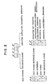
- the memory 2200 stores these events in the form of 4-bit information in correspondence to each instruction or operand address.
- the 4-bit information has the following meaning. Bit 2 0 is assigned to "instruction execution” information, bit 2 is assigned to “successful branching” information, bit 2 2 is assigned to “main storage reference” information, and bit 2 3 is assigned to "main storage change" information.
- the instruction executional information is recorded in the memory 2200 at locations corresponding to addresses of instructions and their operands.
- a new set of information is recorded on a logical-sum basis with information which is already recorded.
- An example of the instruction executional event record is shown in Fig. 3, in which a set of instruction executional information (including information on successful or unsuccessful branching of a branch instruction) is recorded at a location in the memory 2200 corresponding to the first address of that instruction word, and main storage reference/change information is recorded for each byte at a location in the memory 2200 corresponding to the address of that byte.
- a set of instruction executional information for a 4-byte instruction word beginning at address 0 is recorded at the location in the memory 2200 corresponding to address 0, with the memory contents at the locations corresponding to addresses 1, 2 and 3 being left unchanged.
- a 4-byte operand at address 20 is subjected to address reference/change in 4-byte units, but its reference/change information is recorded for each byte at corresponding location in the memory 2200.
- the recording operation for instruction executional events is controlled by the instruction event recording controller 2100.
- the controller 2100 controls the overall instruction monitor 2000 in accordance with information stored as instruction event recording control words (will be termed RCW hereinafter).
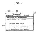
- the RCW has entries as shown in Fig. 4, and they can be set arbitrarily through the execution of the special commands (will be termed "instruction monitor control commands" hereinafter) by the central processor 1000.
- Record type 211 in Fig. 4 is an 8-bit field for specifying events to be recorded by the instruction monitor, and bit assignment is as shown in Table 1.
- bit 0 With bit 0 being “l”, execution of an instruction or successful or unsuccessful branching of a branch instruction is recorded, and with bit 1 being “1", main storage reference/change is recorded. These two bits can be "1" at the same time. With bit 2 being “1”, instruction executional events are recorded only when the central processor 1000 is in address non-translation mode, while with bit 3 being “1”, instruction executional events are recorded only when the processor is in address translation mode. In case a virtual machine system operates in the central processor with bit 4 being “1”, instruction executional events of VMCP, which is the control program of the virtual machine system, are collected, while with bit 5 being “1”, instruction executional events of OS operating in the virtual machine system are recorded. If more than one bit among bit 2 through bit 5 is "1", a logical product of specified conditions becomes the recording condition.
- Number of areas 212 in Fig. 4 is an 8-bit field for specifying the number of areas under event recording (i.e., monitor areas). The field takes values 1 through 255.
- Each of monitor areas is represented by a pair of data in monitor area list 213, and the pair of data indicate the starting and ending addresses of the monitor area.
- the memory 2200 is logically partitioned in number specified as the number of areas 212 (each memory section is called an area), and each area corresponds to a monitor area specified in the monitor area list 213.
- This command is used to commence the instruction executional event recording operation in accordance with the RCW contents which have been set.
- This command is used to halt the instruction executional event recording operation.
- This command is used to load the control information specified in the operand of this command into RCW.
- the command checks as to whether the capacity of the memory 2200 is sufficient to record instruction executional information for all specified monitor areas, and if it is found negative the command sets "1" in the condition code for the result of execution of this command.
- This command is used to read out instruction executional information recorded in the memory 2200 into the main storage at the location specified by the operand.
- Execution of this command halts the instruction executional event recording operation and clears the memory 2200 and the control registers in the event recording controller 2100.
- This command checks the connection of the instruction monitor, and if it is found disconnected the command sets "2" in the condition code for the result of execution of this command. If the monitor is found connected, the command writes the capacity of the memory 2200 and the like into the main storage.
- Fig. 5 shows in further detail the instruction event recording controller 2100.
- the controller 2100 incorporates a microprogram-based control unit 200 for controlling the recording operation of instruction executional events, an RCW 210, an instruction address register 220 for holding the instruction address, an operand address register pair 230-A and 230-B for holding the operand addresses of the instruction, an operand length register pair 240-A and 240-B for holding the lengths of the operands, an instruction execution bit register 250 for recording the completion of execution of an instruction, an operation bit register 280 indicating the consistence of the event recording condition indicated by the bits 2 through 5 of the record type 211 with the operational mode of the central processor, a memory address register 260 indicating the address of the memory 2200, and an area origination register 270 indicating the originating addresses of the partitioned areas in the memory 2200.
- a microprogram-based control unit 200 for controlling the recording operation of instruction executional events
- an RCW 210 for controlling the recording operation of instruction executional events
- the instruction address register 220, operand register pair 230-A,B and operand length register pair 240-A,B are provided in the same number as the number of instruction types under pipeline preceding control.
- the area origination register 270 is set to a value calculated using the values of the monitor area list 213 when the RCW load command is executed.
- the operation of the instruction event recording controller 2100 will be described.
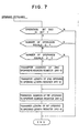
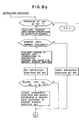
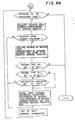
- the instruction executional event recording operation takes place in synchronism with the following three pipeline stages of the central processor as shown in the flowcharts of Figs. 6, 7 and 8, respectively.
- the instruction control unit 1100 calculates the address of the instruction word, and it is read out of the main storage.
- the instruction address and the central processor operating mode are indicated through the signal line 1101, interface unit 1300 and signal line 1001 to the event recording controller 2100, which then implements the following operations basing on the operational mode of the central processor and the address of the instruction word.
- the instruction executional information (including information on successful or unsuccessful branching of a branch instruction) and the main storage reference/change information are indicated through the signal line 1201, interface unit 1300 and signal line 1001 to the event recording controller 2100.
- the event recording: controller 2100 implements the following processings.
- Information recorded as described above is transferred to the main storage by the memory read command and outputted on the printer or the like on request so that it is used to check whether the program test has been conducted in a sufficient range and also used for the debugging of the program.
- the instruction monitor is controlled (for record starting, halting, etc.) by the command (i)-(vii) executed by the central processor
- this control may alternatively be implemented externally (e.g., by manual operation) through the console, service processor and the like, or the system may be made operative in both control modes.
- the specialty hardware arrangement of the above embodiment may be replaced with a software-based system using a fast-operating microprocessor for implementing the foregoing processings.
- the recording means (memory 2200 in the above embodiment) may be substituted by part of the main storage.
- the present invention is also applicable to a pseudo program such as an I/O channel program.
- the present invention enables collection and recording of instruction executional events including successful or unsuccessful branching of branch instructions as well as execution of instructions concurrently with the execution of these instructions without the need of modification for the program under test, whereby information necessary and sufficient for the evaluation of perfection of the program test can readily be obtained.
Landscapes
- Engineering & Computer Science (AREA)
- General Engineering & Computer Science (AREA)
- Theoretical Computer Science (AREA)
- Computer Hardware Design (AREA)
- Quality & Reliability (AREA)
- Physics & Mathematics (AREA)
- General Physics & Mathematics (AREA)
- Debugging And Monitoring (AREA)
Applications Claiming Priority (2)
| Application Number | Priority Date | Filing Date | Title |
|---|---|---|---|
| JP60106044A JPS61264447A (ja) | 1985-05-20 | 1985-05-20 | 命令実行事象記録装置 |
| JP106044/85 | 1985-05-20 |
Publications (2)
| Publication Number | Publication Date |
|---|---|
| EP0202628A2 true EP0202628A2 (fr) | 1986-11-26 |
| EP0202628A3 EP0202628A3 (fr) | 1989-06-14 |
Family
ID=14423634
Family Applications (1)
| Application Number | Title | Priority Date | Filing Date |
|---|---|---|---|
| EP86106709A Withdrawn EP0202628A3 (fr) | 1985-05-20 | 1986-05-16 | Moniteur d'instruction à l'usage d'un processeur de données à programme accumulé |
Country Status (2)
| Country | Link |
|---|---|
| EP (1) | EP0202628A3 (fr) |
| JP (1) | JPS61264447A (fr) |
Cited By (4)
| Publication number | Priority date | Publication date | Assignee | Title |
|---|---|---|---|---|
| GB2200482A (en) * | 1987-01-22 | 1988-08-03 | Nat Semiconductor Corp | Monitoring control flow in a microprocessor |
| EP0353886A3 (fr) * | 1988-08-02 | 1991-07-10 | International Business Machines Corporation | Impression des parcours d'exécution de programme dans un système à calculateur |
| US5121489A (en) * | 1988-08-02 | 1992-06-09 | International Business Machines Corporation | Tracing method for identifying program execution paths using a trace points bit map with one-to-one correspondence with embedded trace points |
| US5758061A (en) * | 1995-12-15 | 1998-05-26 | Plum; Thomas S. | Computer software testing method and apparatus |
Family Cites Families (2)
| Publication number | Priority date | Publication date | Assignee | Title |
|---|---|---|---|---|
| US3673573A (en) * | 1970-09-11 | 1972-06-27 | Rca Corp | Computer with program tracing facility |
| JPS603756A (ja) * | 1983-06-21 | 1985-01-10 | Meidensha Electric Mfg Co Ltd | プログラム試験装置 |
-
1985
- 1985-05-20 JP JP60106044A patent/JPS61264447A/ja active Pending
-
1986
- 1986-05-16 EP EP86106709A patent/EP0202628A3/fr not_active Withdrawn
Cited By (5)
| Publication number | Priority date | Publication date | Assignee | Title |
|---|---|---|---|---|
| GB2200482A (en) * | 1987-01-22 | 1988-08-03 | Nat Semiconductor Corp | Monitoring control flow in a microprocessor |
| GB2200482B (en) * | 1987-01-22 | 1991-09-04 | Nat Semiconductor Corp | Integrated-circuit microprocessor and method of monitoring control flow therein |
| EP0353886A3 (fr) * | 1988-08-02 | 1991-07-10 | International Business Machines Corporation | Impression des parcours d'exécution de programme dans un système à calculateur |
| US5121489A (en) * | 1988-08-02 | 1992-06-09 | International Business Machines Corporation | Tracing method for identifying program execution paths using a trace points bit map with one-to-one correspondence with embedded trace points |
| US5758061A (en) * | 1995-12-15 | 1998-05-26 | Plum; Thomas S. | Computer software testing method and apparatus |
Also Published As
| Publication number | Publication date |
|---|---|
| EP0202628A3 (fr) | 1989-06-14 |
| JPS61264447A (ja) | 1986-11-22 |
Similar Documents
| Publication | Publication Date | Title |
|---|---|---|
| US5134701A (en) | Test apparatus performing runtime replacement of program instructions with breakpoint instructions for processor having multiple instruction fetch capabilities | |
| US5274811A (en) | Method for quickly acquiring and using very long traces of mixed system and user memory references | |
| US4937740A (en) | Real time software analyzing system for storing selective m-bit addresses based upon correspondingly generated n-bit tags | |
| US4253183A (en) | Method and apparatus for diagnosing faults in a processor having a pipeline architecture | |
| US4485440A (en) | Central processor utilization monitor | |
| US4205370A (en) | Trace method and apparatus for use in a data processing system | |
| US20020013893A1 (en) | Real time debugger interface for embedded systems | |
| US5289587A (en) | Apparatus for and method of providing the program counter of a microprocessor external to the device | |
| EP0111952B1 (fr) | Vérification de l'architecture d'un processeur ayant un jeu d'instruction partiel | |
| EP0141744A2 (fr) | Méthode et dispositif pour l'auto-test de processeurs à accélérateur de calcul à virgule flottante | |
| US4040037A (en) | Buffer chaining | |
| US5819024A (en) | Fault analysis system | |
| JPH0749799A (ja) | 自動化装置および方法 | |
| EP0309793A2 (fr) | Méthode et appareil de test d'un circuit intégré comprenant un microprocesseur et une antémémoire d'instructions | |
| JPS61264447A (ja) | 命令実行事象記録装置 | |
| JPS6383841A (ja) | プログラムテスト可能な計算機中央処理装置 | |
| US20070226471A1 (en) | Data processing apparatus | |
| JP2868114B2 (ja) | 監視診断機能付計算機 | |
| JPH06342387A (ja) | 情報処理装置に於ける障害情報採取方式 | |
| GB1264066A (fr) | ||
| KR960003052B1 (ko) | 내장된 캐쉬 메모리 유니트를 가진 마이크로프로세서 | |
| JPS61161557A (ja) | プログラム・デバツグ方法および装置 | |
| JP2001265619A (ja) | データトレース方式 | |
| JPH03204044A (ja) | カバレージ測定方法及びマイクロコンピュータ | |
| JPS59153246A (ja) | デバツグアシスト装置 |
Legal Events
| Date | Code | Title | Description |
|---|---|---|---|
| PUAI | Public reference made under article 153(3) epc to a published international application that has entered the european phase |
Free format text: ORIGINAL CODE: 0009012 |
|
| AK | Designated contracting states |
Kind code of ref document: A2 Designated state(s): DE FR GB |
|
| PUAL | Search report despatched |
Free format text: ORIGINAL CODE: 0009013 |
|
| AK | Designated contracting states |
Kind code of ref document: A3 Designated state(s): DE FR GB |
|
| STAA | Information on the status of an ep patent application or granted ep patent |
Free format text: STATUS: THE APPLICATION IS DEEMED TO BE WITHDRAWN |
|
| 18D | Application deemed to be withdrawn |
Effective date: 19890601 |
|
| RIN1 | Information on inventor provided before grant (corrected) |
Inventor name: YOSHIZAWA, YASUFUMI Inventor name: WAKAI, KATSURO Inventor name: IMURA, JUNICHI Inventor name: SATOH, TAKAO Inventor name: KUBO, TAKASHIGE |