EP0251739A2 - Appareil à copier en couleurs - Google Patents
Appareil à copier en couleurs Download PDFInfo
- Publication number
- EP0251739A2 EP0251739A2 EP87305725A EP87305725A EP0251739A2 EP 0251739 A2 EP0251739 A2 EP 0251739A2 EP 87305725 A EP87305725 A EP 87305725A EP 87305725 A EP87305725 A EP 87305725A EP 0251739 A2 EP0251739 A2 EP 0251739A2
- Authority
- EP
- European Patent Office
- Prior art keywords
- color
- ink
- signals
- amount
- corrected
- Prior art date
- Legal status (The legal status is an assumption and is not a legal conclusion. Google has not performed a legal analysis and makes no representation as to the accuracy of the status listed.)
- Granted
Links
- 238000012937 correction Methods 0.000 claims description 14
- 239000000976 ink Substances 0.000 claims 25
- 238000004042 decolorization Methods 0.000 abstract description 12
- 239000003086 colorant Substances 0.000 abstract description 9
- 238000010586 diagram Methods 0.000 description 8
- 230000006870 function Effects 0.000 description 8
- 239000000872 buffer Substances 0.000 description 5
- 238000000034 method Methods 0.000 description 4
- 238000006243 chemical reaction Methods 0.000 description 3
- 239000007787 solid Substances 0.000 description 2
- 230000003750 conditioning effect Effects 0.000 description 1
- 238000004519 manufacturing process Methods 0.000 description 1
Images















Classifications
-
- H—ELECTRICITY
- H04—ELECTRIC COMMUNICATION TECHNIQUE
- H04N—PICTORIAL COMMUNICATION, e.g. TELEVISION
- H04N1/00—Scanning, transmission or reproduction of documents or the like, e.g. facsimile transmission; Details thereof
- H04N1/46—Colour picture communication systems
- H04N1/56—Processing of colour picture signals
- H04N1/60—Colour correction or control
- H04N1/6016—Conversion to subtractive colour signals
- H04N1/6022—Generating a fourth subtractive colour signal, e.g. under colour removal, black masking
- H04N1/6025—Generating a fourth subtractive colour signal, e.g. under colour removal, black masking using look-up tables
Definitions
- This invention is a circuit for the automatic color-correction of the output of a color raster input scanner (RIS) to allow the production of an accurate color rendition of a copy produced therefrom by a color raster output scanner (ROS) , the circuit specifically comprising a set of look-up tables for the conversion of the red, green and blue inputs from the RIS to the cyan, magenta, yellow and black output of the ROS.
- RIS color raster input scanner
- ROS color raster output scanner
- Color copiers may convert the scanned input signals into color copies, but the colors are only approximate over the total range of densities.
- Cyan is computed as a constant times red minus a constant times green minus a constant times blue.
- magenta is a function of green, red and blue, and yellow is a function of blue, red and green.
- a complicating factor is that , for the best color rendition, a process known in the industry as "under color removal" is also required. Simply stated, the process is to first find which of the three output colors is using the least ink. For a numerical example, assume that the output scanner has computed an output comprising one and a half units of cyan ink, three units of magenta and three units of yellow. Then the least ink is one and one half units. The next step is to subtract a fraction of that amount of least ink from all three colors, and substitute an equal amount of black ink. In the numerical example, assume that the amount of color removed is seven tenths of the color over an original threshold of one half a unit.
- the final amounts of ink will be 0.8 units of cyan, 2.3 units of magenta, 2.3 units of yellow and 0.7 units of black. It is only after this computation is accomplished that the amount of any color ink is known.
- a circuit comprising three color-correction tables stored in RAM is provided.
- Each look-up table is 256 words to provide a smooth conversion over the range of values.
- two summing devices are used to subtract the two negative values from the positive term.
- the under color removal is then computed by determining, in a set of comparators, which color has the least ink.
- An additional look-up table is used to determine the actual amount of ink removed, a summing circuit performs the subtraction, and the actual amount of ink to be used is finally determined.
- the circuit is arranged in the form of a pipe line so that the entire computation for each spot can take place at reasonable real-time speeds.
- the system is also implemented so that the amount of ink used during the black cycle may be more or less than the amount of color ink removed during the color cycles. Therefore, two additional RAM tables are required, one for color ink removal and one for the amount of black ink to be used.
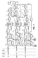
- Channel # 1 processes cyan as a function of red, green and blue
- channel #2 processes magenta as a function of green, blue and red
- channel #3 generates yellow as a function of blue, red and green.
- the three inputs are signals which are functions of red, green and blue, as shown.
- the three tables 28, 37 and 44 are loaded with constants , 256 constants in each table, each constant 8 bits in length. Since there are three color revolutions per copy, the tables are reloaded before each revolution of the printing drum to load the correct table values. There are thus a total of 27 sets of color values that are periodically loaded into the nine tables, nine at a time at the beginning of each of three color revolutions, plus two sets of black values.
- an eight-bit differential digital signal carried on sixteen lines, representing the amount of red the RIS has picked up, is coupled to a first latch/register 23 which is used as a buffer.
- the output is coupled to a 2:1 multiplexer 25 which can select either this red signal or a data test value from latch 24.
- the output of the multiplexer 25 is coupled to the next multiplexer 26 which selects the red signal from multiplexer 25.
- the RAM is loaded at the start of each color revolution the address is forced on the RAM IC through this buffer, along with the constant on the RAM data input lines to create a table in RAM. In a test mode there will be an address from a buffer 27 coupled to the RAM 28.
- the signal is applied to the RAM , a 256 by 8-bit memory that will output the red table output term.
- the next three shift registers 29, 30 and 31 are inserted in the path for timing purposes.
- the green input is applied in a similar manner to circuit elements 32 through 38, and a blue input is applied to circuit elements 39 through 45.
- the bottom two parts of the circuit are configured so that the outputs are negative values which are added in summer 46 to give a negative value. Then, this negative value is added to the positive output of shift register 31 in summer 47 to give a value of cyan, which is coupled through multiplexers 48, 49 and 50 to become the board output for cyan.
- the first multiplexer 48 is configured to prevent underflow, and the second 49 is to prevent overflow. That is to say, large negative values are prevented from becoming more negative and finally underflowing to become a large positive number, and large positive numbers are prevented from increasing to an overflow and becoming a large negative number.
- the final multiplexer 50 selects between a test value or this final cyan value. Shift registers 51, 29, 30 and 31 are provided to adjust the timing between circuit paths.
- Two identical circuit boards generate magenta and yellow signals, and all three are applied to the under color removal circuit of Fig. 2.
- the cyan signal is applied through line receiver 60 and register 61 to comparators 66 and 68.
- the magenta signal is applied through line receiver 62 and register 63 to comparators 67 and 66, and the yellow signal is applied through line receiver 64 and register 65 to comparators 68 and 67.
- the comparators will couple out an indication of which of its two inputs has the higher value, which corresponds to the least ink.
- the identity of the higher source is coupled to the selector 69 which identifies the source of the highest value,the least ink value, through register 70 to the 3:1 multiplexer 71.
- the cyan, magenta and yellow values are respectively coupled through registers 92, 93 and 94 to the same multiplexer 71.
- the identity of the least ink channel is coupled to the multiplexer 71, it selects the corresponding output of one of the three registers 92, 93 or 94.
- the highest value is coupled through the multiplexer 71, through multiplexer 72 (which is used to couple addresses to the RAM 73 during the loading of table values) to the color table contained in RAM 73.
- the multiplier 72 serves the same basic functions as the multiplexers 26, 35 and 43 for the color tables. This table has values which reflect both the threshold and factor for color removal, and therefore represents the amount of ink that should be removed.
- original color values are also applied to a 4:1 multiplexer 74.
- the color that is being printed during the current revolution of the printer drum (cyan, magenta, yellow or black) is selected.
- the current color, coupled through registers 75 and 76 and the color to be removed coupled through register 77 are applied to negative adder 78 which performs the subtraction to produce the amount of ink to be used for the current spot to be printed. This is coupled out to the printer by multiplexer 83.
- This multiplier factor is controlled by the table in the Ram 82, the output of which is selected by the multiplexer 83 during solid color printing cycles.
- the path along the bottom of the Figure through line receiver 79 and register 80 is used for black computer generated graphics only, and the RAM color tables 73 and 82 are not used.
- the output can be coupled through multiplexer 86 and converted to analog by converter 87 so that it can be viewed on an oscilloscope.
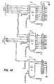
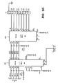
- Fig 3 is one of three identical circuits that supplies either red, green or blue signals to the three channels.
- the least-significant bit of the input is represented in this figure by the "R0" and “not R0" lines.
- These eight sets of two inputs are presented to a set of differential input gates 100 through 107, the outputs of which are coupled through buffers 108, 109 to the remainder of the circuit as either positive values or negative values, as are the corresponding outputs of the other two sets of gates and buffers that supply the green and blue signals.
- the signal lines are terminated at the end of the lines after being coupled through three boards each.
- the cabling between boards is arranged so that the red, green and blue signals are wired into the channels either as positive or negative signals depending on whether the channels require them as primary or secondary colors, as shown in the left-hand edge of Fig 1.
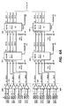
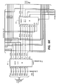
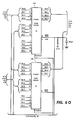
- Fig 4 is a detailed schematic diagram of that portion of Fig 1 which is beneath the dotted line, which is labelled "#2 Card” and which comprises the two color-correction tables 37 and 44.
- one input color is supplied as differential input signals C2-0 through C2-7 in both positive and negative form to line receivers 32a through 32h, which correspond to line receiver 32 of Fig 1.
- the other color is supplied at input pins C3-0 through C3-7, positive and negative, to line receivers 39a through 39h which correspond to line receiver 39 of Fig 1.
- the line receiver outputs go to multiplexers 34a, 34b, 41a and 41b, which switch between the actual color signals or test values.
- the signals are supplied to multiplexers 35a, 35b, 43a and 43b which decide between the the color signals or RAM address data, to be used when initially loading the tables.
- the output of these multiplexers is connected to the color-correction RAMs 37a, 37b, 44a and 44b, which generate the two negative color-correction terms. These terms are coupled through shift registers 38 and 45 to the summer comprising summing devices 46a and 46b, to add the two negative values.
- the final output which may be as much as a nine bit number resulting from the addition of two eight bit numbers, is coupled out of the board by multiplexers 51a, 51b and 51c which operate as a nine bit shift register.
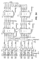
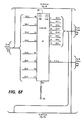
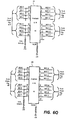
- Fig 5 is a schematic diagram of that portion of Fig 1 above the dotted line, referred to as "#1 Card".
- the primary color of the channel is received as eight sets of differential inputs C1-0 through C1-7 at the inputs of a line receiver comprising gates 23a through 23 h.
- the output then goes to multiplexer 25a, 25b, which decides between the color input and test value data.
- the data is then coupled to multiplexer 26a, 26b which switches between RAM 28a-c addresses during table loading or the color values during operation.
- the output from the RAM 28a-c is a ten-bit value to preserve accuracy. That is to say, the nine-bit negative value of board # 2 must be subtracted from the value output by the color-correction table 28 without the loss of any least-significant bits. Therefore, a ten-bit value is output from the Color-correction Table comprising RAM devices 28a, 28b and 28c, and is coupled through the three shift registers 29ab, 30ab and 31ab to the summer 47a and 47b. Unless otherwise noted, shift registers and multiplexers are provided to establish timing relationships.
- the sum of these two negative values is input to this board at line receivers 52a through 52i, and from there through shift register 52j to the summer 47a and 47b, the nine-bit output of which is coupled through multiplexer 48a, 48b which is wired to prevent underflow, and 49a 49b, which is wired to prevent overflow.
- the final device is a multiplexer 50a, 50b, which switches between the color value or a test value.
- the above-mentioned underflow can occur when there is a small amount of a primary color from which a large amount of secondary color may be subtracted. If left uncorrected, the result would be underflow which would result in a large positive value instead of a zero value.
- Multiplexer 48a 48b was included to prevent this.
- Overflow is similarly the addition of two values which would otherwise result in a number greater than 255, and is prevented by multiplexer 49a and 49b. More specifically, the overflow bit is used as the switching input to the multiplexer. If the bit is zero, the multiplexer switches in the color value. If the bit is a one, the multiplexer is forced to use as an input a hard-wired maximum positive number. Therefore, in all cases the output is positive. Underflow is similarly prevented by switching between the color value or zero.
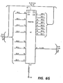
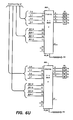
- the three sets of color-correction boards output three eight-bit digital signals representing cyan, magenta and yellow, all of which go to the under color removal board, a schematic diagram of which is shown as Fig 6.
- the cyan signal in the form of eight differential bits is input to line receivers 60a through 60h.
- the magenta signal is input to line receivers 62a-h, and the yellow is received at line receivers 64a-h.
- the fourth line receiver in the figure , 79a-h receives the solid color computer-generated graphics signal.
- the four signals are coupled through shift registers 80, 61, 63 and 65, and then the three color signals are input to the comparators 66, 67, 68, which all operate in an identical manner.
- comparator 67 in the schematic, an eight-bit magenta signal is applied to the left inputs, an eight-bit yellow signal is applied to the right inputs, and one output line, pin 8, goes high or low to indicate which is greater, the higher number indicating less ink.
- the three comparator output lines go to the multiplexer 69 which produces a two-bit output identifying the color having the least ink. This output is coupled through shift register 70, and is then used to control multiplexer 71a-c.
- the three eight-bit color values from shift registers 61, 63 and 65 are coupled through shift registers 92, 93 and 94 and are applied to the inputs of the same multiplexer 71a-c, which, under the control of the two lines from shift register 70, outputs the eight-bit signal corresponding to the amount of least ink of the three color signals.
- This signal is then coupled through multiplexer 72a, 72b which switches between this color signal or address data for loading the RAMs 73, 82, and is then used as an input to the color table RAM 73, the output of which is a number corresponding to the amount of ink that should be removed from all three color channels. This number is coupled through shift register 77, and becomes one input to the adder 78a, 78b.
- the three color signals that are coupled through shift registers 92, 93 and 94, and the computer-generated black signal which is coupled through line receivers 79a through 79h, are used as inputs to the multiplexer 74a-c, which is controlled to select the color currently being printed.
- This output is coupled through shift registers 75 and 76 and becomes the other input to adder 78a, 78b, which is actually wired to subtract the two input values.
- the result is that the amount of ink that must be removed is subtracted from the color currently being printed to result in the final amount of ink to be used to print the current dot.
- This final value, which is the output of adder 78a, 78b, is coupled out through multiplexer 83a, 83b, which can switch between this color signal from RAM 73 or the black signal from RAM 82.
- the least-ink signal output from shift register 72 is used as an input to the black table RAM 82a, 82b, the output of which is the amount of black ink to be used.
- This system is implemented so that the amount of ink removed from the three color channels may be different from the amount of black ink used during the black cycle.
- the second RAM 82a, 82b is used to hold this second set of values. These do not go through any further conditioning, but are coupled directly out through shift register 84, and the output multiplexer 83a, 83b.
- a second multiplexer 86a, 86b is used to switch the output signals to an A/D converter for the convenience of the test operator.
- This system may be used without under color removal. That is, the cyan, magenta and yellow outputs from the circuit of Figure 1 can be used directly to drive the printer.
Landscapes
- Engineering & Computer Science (AREA)
- Multimedia (AREA)
- Signal Processing (AREA)
- Color Image Communication Systems (AREA)
- Dot-Matrix Printers And Others (AREA)
- Color, Gradation (AREA)
- Color Electrophotography (AREA)
- Facsimile Image Signal Circuits (AREA)
Applications Claiming Priority (2)
| Application Number | Priority Date | Filing Date | Title |
|---|---|---|---|
| US880241 | 1986-06-30 | ||
| US06/880,241 US4763190A (en) | 1986-06-30 | 1986-06-30 | Digital color correction circuit |
Publications (3)
| Publication Number | Publication Date |
|---|---|
| EP0251739A2 true EP0251739A2 (fr) | 1988-01-07 |
| EP0251739A3 EP0251739A3 (en) | 1989-08-30 |
| EP0251739B1 EP0251739B1 (fr) | 1994-01-19 |
Family
ID=25375819
Family Applications (1)
| Application Number | Title | Priority Date | Filing Date |
|---|---|---|---|
| EP87305725A Expired - Lifetime EP0251739B1 (fr) | 1986-06-30 | 1987-06-26 | Appareil à copier en couleurs |
Country Status (4)
| Country | Link |
|---|---|
| US (1) | US4763190A (fr) |
| EP (1) | EP0251739B1 (fr) |
| JP (1) | JPS6313580A (fr) |
| DE (1) | DE3788827T2 (fr) |
Cited By (1)
| Publication number | Priority date | Publication date | Assignee | Title |
|---|---|---|---|---|
| EP0389748A3 (fr) * | 1989-03-31 | 1991-01-23 | Eastman Kodak Company | Interface flexible de mise en forme pour le transfert de données d'images |
Families Citing this family (14)
| Publication number | Priority date | Publication date | Assignee | Title |
|---|---|---|---|---|
| JP2712293B2 (ja) * | 1988-05-24 | 1998-02-10 | 富士ゼロックス株式会社 | カラー画像編集装置 |
| JPH02118680A (ja) * | 1988-10-28 | 1990-05-02 | Fuji Xerox Co Ltd | 画像形成装置の下色除去方式 |
| JP2810392B2 (ja) * | 1988-12-21 | 1998-10-15 | キヤノン株式会社 | 記録装置 |
| JPH02178656A (ja) * | 1988-12-28 | 1990-07-11 | Fuji Photo Film Co Ltd | 下色除去方法及びその装置 |
| US5657395A (en) * | 1989-03-02 | 1997-08-12 | Minolta Camera Kabushiki Kaisha | Image processing device providing improved image data processing by converting original image into a plurality of pixels and analyzing density data of each pixel |
| US5398124A (en) * | 1991-06-29 | 1995-03-14 | Minolta Camera Kabushiki Kaisha | Image processor |
| US5515479A (en) * | 1992-07-23 | 1996-05-07 | Xerox Corporation | Image processing method to reduce marking material coverage in printing processes |
| US5519815A (en) * | 1993-11-29 | 1996-05-21 | Xerox Corporation | Image processing method to reduce marking material coverage in printing processes |
| US5649071A (en) * | 1994-09-26 | 1997-07-15 | Xerox Corporation | Image processing method to reduce marking material coverage in sequential color printing processes |
| US5831748A (en) * | 1994-12-19 | 1998-11-03 | Minolta Co., Ltd. | Image processor |
| US6574010B1 (en) * | 1995-07-31 | 2003-06-03 | Canon Kabushiki Kaisha | Image processing apparatus and method |
| US6081340A (en) * | 1997-03-31 | 2000-06-27 | Xerox Corporation | Image processing method to reduce marking material coverage with non-linear specifications |
| US6198543B1 (en) * | 1998-02-05 | 2001-03-06 | Canon Kabushiki Kaisha | Color table look-up using compressed image data |
| US6973843B2 (en) * | 2002-01-08 | 2005-12-13 | Iowa State University Research Foundation, Inc. | Method of measuring flow rate of flowable material under continuous flow conditions, and an in-line continuous flow meter |
Family Cites Families (19)
| Publication number | Priority date | Publication date | Assignee | Title |
|---|---|---|---|---|
| US2231668A (en) * | 1938-06-25 | 1941-02-11 | Eastman Kodak Co | Electric circuit |
| US3555262A (en) * | 1968-05-07 | 1971-01-12 | Dainippon Screen Mfg | Apparatus for production of color separation records |
| JPS55142345A (en) * | 1979-04-23 | 1980-11-06 | Dainippon Screen Mfg Co Ltd | Masking operation method in digital color tone control |
| IL59886A (en) * | 1979-04-23 | 1983-06-15 | Dainippon Screen Mfg | Digital color control method and machine |
| WO1982000902A1 (fr) * | 1980-09-10 | 1982-03-18 | Klie J | Procede et circuit pour la correction partielle du dessin lors de la reproduction d'images en couleur |
| DE3109190C2 (de) * | 1981-03-11 | 1985-07-11 | Dr.-Ing. Rudolf Hell Gmbh, 2300 Kiel | Verfahren zur Reproduktion farbiger Vorlagen im Vierfarbendruck unter Farbrücknahme |
| IL67202A0 (en) * | 1981-12-07 | 1983-03-31 | Xerox Corp | Apparatus and method for color adjustment of digital displays |
| US4476487A (en) * | 1982-05-04 | 1984-10-09 | Dr. -Ing. Rudolf Hell Gmbh | Method and circuit arrangement for partial electronic retouch in color image reproduction |
| JPS5972869A (ja) * | 1982-10-20 | 1984-04-24 | Canon Inc | カラ−画像形成装置におけるマスキング処理方法 |
| US4631578A (en) * | 1983-03-04 | 1986-12-23 | Canon Kabushiki Kaisha | Method of and apparatus for forming a color picture using a plurality of color correction processings |
| JPS59161980A (ja) * | 1983-03-06 | 1984-09-12 | Canon Inc | 画像処理装置 |
| US4682216A (en) * | 1983-03-08 | 1987-07-21 | Canon Kabushiki Kaisha | Color image picture forming process and apparatus which improves the quality of the black portions of the picture |
| JPS6043968A (ja) * | 1983-08-22 | 1985-03-08 | Ricoh Co Ltd | 色補正回路 |
| ATE29816T1 (de) * | 1983-12-14 | 1987-10-15 | Hell Rudolf Dr Ing Gmbh | Verfahren und schaltungsanordnung zur selektiven korrektur von farbtoenen und farben. |
| JPS60132463A (ja) * | 1983-12-21 | 1985-07-15 | Canon Inc | カラ−プリンタ |
| GB2154094B (en) * | 1983-12-30 | 1988-10-12 | Dainippon Screen Mfg | A multi-colour printing process |
| JPH067664B2 (ja) * | 1984-02-29 | 1994-01-26 | キヤノン株式会社 | カラー画像信号処理装置 |
| JPS60236576A (ja) * | 1984-05-10 | 1985-11-25 | Fuji Xerox Co Ltd | 色再現マスキング方法及び装置 |
| JPS6148276A (ja) * | 1984-08-16 | 1986-03-08 | Ricoh Co Ltd | 色補正回路 |
-
1986
- 1986-06-30 US US06/880,241 patent/US4763190A/en not_active Expired - Fee Related
-
1987
- 1987-06-25 JP JP62159540A patent/JPS6313580A/ja active Pending
- 1987-06-26 DE DE3788827T patent/DE3788827T2/de not_active Expired - Fee Related
- 1987-06-26 EP EP87305725A patent/EP0251739B1/fr not_active Expired - Lifetime
Cited By (1)
| Publication number | Priority date | Publication date | Assignee | Title |
|---|---|---|---|---|
| EP0389748A3 (fr) * | 1989-03-31 | 1991-01-23 | Eastman Kodak Company | Interface flexible de mise en forme pour le transfert de données d'images |
Also Published As
| Publication number | Publication date |
|---|---|
| DE3788827T2 (de) | 1994-06-16 |
| US4763190A (en) | 1988-08-09 |
| EP0251739A3 (en) | 1989-08-30 |
| EP0251739B1 (fr) | 1994-01-19 |
| DE3788827D1 (de) | 1994-03-03 |
| JPS6313580A (ja) | 1988-01-20 |
Similar Documents
| Publication | Publication Date | Title |
|---|---|---|
| EP0251739B1 (fr) | Appareil à copier en couleurs | |
| EP0448330B1 (fr) | Procédé et appareil de traitement d'image | |
| US4739397A (en) | Image processing apparatus in which the operating mode of either a color or monochromatic image data processing means is set by command data prior to receipt of either color or monochromatic image data | |
| EP0205332B1 (fr) | Modifications de couleurs dans des systèmes de reproduction d'images | |
| US5719956A (en) | Image processing apparatus with separate color conversion for CMY signals and K signal | |
| CA1338342C (fr) | Appareil de traitement d'images | |
| US8306321B2 (en) | Image processing method of compressing image data to be suitable for data transmission | |
| JP2919174B2 (ja) | ラスター出力装置上に画像を出力するための出力データの生成方法 | |
| GB2132052A (en) | A method and system for processing image data | |
| JP2746939B2 (ja) | 色変換装置 | |
| US7411707B2 (en) | Image processing apparatus and method thereof | |
| EP0376209A2 (fr) | Procédé et appareil pour l'enlèvement de sous-couleurs | |
| EP0643528A2 (fr) | Appareil de traitement d'image capable de réaliser un marquage d'édition | |
| EP0162500B1 (fr) | Procédé et circuit pour produire des signaux d'arrière-plan en couleur | |
| EP0350919A2 (fr) | Appareil de production d'images à couleurs | |
| EP0175066B1 (fr) | Méthode pour la correction de signaux de séparation de couleur | |
| US4954888A (en) | Apparatus for reading and digital processing of color images | |
| EP0475362B1 (fr) | Appareil de traitement d'images pour déterminer la proportion d'enlèvement de la sous-couleur | |
| JP2603277B2 (ja) | カラー画像処理装置 | |
| JPH04346571A (ja) | 黒置換方法及び黒置換処理回路 | |
| JP2954257B2 (ja) | 色情報変換装置 | |
| KR0146904B1 (ko) | 영상신호 처리시스템의 색공간 변환장치 | |
| JPS621368A (ja) | カラ−画像記録における記録色情報補正方法 | |
| EP0598583A2 (fr) | Appareil et procédé de traitement d'images | |
| JPH04241570A (ja) | 印刷装置 |
Legal Events
| Date | Code | Title | Description |
|---|---|---|---|
| PUAI | Public reference made under article 153(3) epc to a published international application that has entered the european phase |
Free format text: ORIGINAL CODE: 0009012 |
|
| AK | Designated contracting states |
Kind code of ref document: A2 Designated state(s): DE FR GB |
|
| PUAL | Search report despatched |
Free format text: ORIGINAL CODE: 0009013 |
|
| AK | Designated contracting states |
Kind code of ref document: A3 Designated state(s): DE FR GB |
|
| 17P | Request for examination filed |
Effective date: 19900222 |
|
| 17Q | First examination report despatched |
Effective date: 19920217 |
|
| GRAA | (expected) grant |
Free format text: ORIGINAL CODE: 0009210 |
|
| AK | Designated contracting states |
Kind code of ref document: B1 Designated state(s): DE FR GB |
|
| REF | Corresponds to: |
Ref document number: 3788827 Country of ref document: DE Date of ref document: 19940303 |
|
| ET | Fr: translation filed | ||
| PLBE | No opposition filed within time limit |
Free format text: ORIGINAL CODE: 0009261 |
|
| STAA | Information on the status of an ep patent application or granted ep patent |
Free format text: STATUS: NO OPPOSITION FILED WITHIN TIME LIMIT |
|
| 26N | No opposition filed | ||
| PGFP | Annual fee paid to national office [announced via postgrant information from national office to epo] |
Ref country code: FR Payment date: 19950609 Year of fee payment: 9 |
|
| PGFP | Annual fee paid to national office [announced via postgrant information from national office to epo] |
Ref country code: GB Payment date: 19950615 Year of fee payment: 9 |
|
| PGFP | Annual fee paid to national office [announced via postgrant information from national office to epo] |
Ref country code: DE Payment date: 19950617 Year of fee payment: 9 |
|
| PG25 | Lapsed in a contracting state [announced via postgrant information from national office to epo] |
Ref country code: GB Effective date: 19960626 |
|
| GBPC | Gb: european patent ceased through non-payment of renewal fee |
Effective date: 19960626 |
|
| PG25 | Lapsed in a contracting state [announced via postgrant information from national office to epo] |
Ref country code: FR Effective date: 19970228 |
|
| PG25 | Lapsed in a contracting state [announced via postgrant information from national office to epo] |
Ref country code: DE Effective date: 19970301 |
|
| REG | Reference to a national code |
Ref country code: FR Ref legal event code: ST |