EP0259878A2 - Elément émetteur d'électrons - Google Patents
Elément émetteur d'électrons Download PDFInfo
- Publication number
- EP0259878A2 EP0259878A2 EP87113260A EP87113260A EP0259878A2 EP 0259878 A2 EP0259878 A2 EP 0259878A2 EP 87113260 A EP87113260 A EP 87113260A EP 87113260 A EP87113260 A EP 87113260A EP 0259878 A2 EP0259878 A2 EP 0259878A2
- Authority
- EP
- European Patent Office
- Prior art keywords
- electron emission
- area
- type semiconductor
- emission element
- electrode
- Prior art date
- Legal status (The legal status is an assumption and is not a legal conclusion. Google has not performed a legal analysis and makes no representation as to the accuracy of the status listed.)
- Granted
Links
Images


Classifications
-
- H—ELECTRICITY
- H01—ELECTRIC ELEMENTS
- H01J—ELECTRIC DISCHARGE TUBES OR DISCHARGE LAMPS
- H01J1/00—Details of electrodes, of magnetic control means, of screens, or of the mounting or spacing thereof, common to two or more basic types of discharge tubes or lamps
- H01J1/02—Main electrodes
- H01J1/30—Cold cathodes, e.g. field-emissive cathode
- H01J1/308—Semiconductor cathodes, e.g. cathodes with PN junction layers
-
- H—ELECTRICITY
- H01—ELECTRIC ELEMENTS
- H01J—ELECTRIC DISCHARGE TUBES OR DISCHARGE LAMPS
- H01J1/00—Details of electrodes, of magnetic control means, of screens, or of the mounting or spacing thereof, common to two or more basic types of discharge tubes or lamps
- H01J1/02—Main electrodes
- H01J1/34—Photo-emissive cathodes
-
- H—ELECTRICITY
- H01—ELECTRIC ELEMENTS
- H01J—ELECTRIC DISCHARGE TUBES OR DISCHARGE LAMPS
- H01J2201/00—Electrodes common to discharge tubes
- H01J2201/34—Photoemissive electrodes
- H01J2201/342—Cathodes
- H01J2201/3421—Composition of the emitting surface
- H01J2201/3423—Semiconductors, e.g. GaAs, NEA emitters
Definitions
- the photoelectric converting junction area composed of the semiconductor area of a conductive type, semiconductor area of opposite conductive type, and conductive area superposed on the transparent electrode, is unified, on the transparent substrate, with an MIM electron emission element composed of said conductive area, insulting area and metal layer.
- the electrode of the photoelectric converting junction area and the conductive area of the MIM electron emission element are used commonly, and an insulating area is provided for electric insulation, and there is thus reached a simple structure enabling integration.
- said photoelectric converting junction area is formed only under the recess of the metal layer, constituting the electron emitting portion of the MIM electron emission element, thereby achieving efficient electron emission.
- the electron emission element is provided with a transparent electrode, a P-type semiconductor area formed on said transparent electrode, and an electrode formed on said P-type semiconductor area, whereby a voltage is applied across said transparent electrode and said electrode, and light is irradiated through said transparent electrode, thereby emitting the electrons generated in said P-type semiconductor from an electron emitting face at an end of said semiconductor area. It is extremely simple in structure, consisting of the P-type semiconductor area and electrodes and allowing light irradiation through the transparent electrode, thereby enabling easy manufacture and high integration.
- the substrate 102 is transparent, and is composed, for example, of glass, ceramics, or an insulating crystal such as GaAs, GaSb, InAs, GaP or spinell (MgAl2O4).
- the conductive area 205 serves as an electrode of the photoelectric converting junction area and also as the conductive layer of the MIM electron emission element, thus simplifying the entire structure.
- the insulating area 206 serves as the insulating layer of the MIM electron emission element, and also insulates the lateral faces of the photoelectric converting junction area, thus preventing the deterioration of characteristic by current leak.
- the photoelectric converting junction area for the photoelectric conversion and the MIM electron emission element for electron emission are mutually superposed and unified to enable high integration, and said junction area is formed only under the recess for electron emission, thereby improving the efficiency thereof. Besides said efficiency is further improved by the presence of area of the work function reducing material 208 in the recess 209. It is therefore rendered possible to produce, in integrated manner, photoexcitable electron emission elements having plural electron sources such as an image sensor.
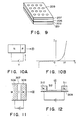
- Fig. 10A is a schematic view of an electron emission element in which a forward bias voltage is applied to a PN junction to inject electrons into the P-layer
- Fig. 10B is a schematic chart showing the current-voltage characteristic thereof.
- transparent electrodes 3011 - 3014 and electrodes 3031 - 3034 are made to cross each other to form a matrix, and a P-type semiconductor area (not shown) is formed at each crossing point.
- a voltage V can be applied to desired P-type semiconductor areas by applying said voltage to desired transparent electrodes 3011 - 3014 and desired electrodes 3031 - 3034 through the control transistors T21 - T24 and T11 - T14.
- the conductive layer 404 is composed of a metal such as Al or a semiconductor such as Si.
- the insulating layer 405 is preferably composed, also from the standpoint of manufacture, of Al2O3 if the conductive layer is composed of Al, or of SiO2 if the conductive layer is composed of Si.
- the metal layer 406 is composed of Al, Au or Pt.
Landscapes
- Cold Cathode And The Manufacture (AREA)
- Common Detailed Techniques For Electron Tubes Or Discharge Tubes (AREA)
Applications Claiming Priority (10)
| Application Number | Priority Date | Filing Date | Title |
|---|---|---|---|
| JP212821/86 | 1986-09-11 | ||
| JP61212821A JPS6369118A (ja) | 1986-09-11 | 1986-09-11 | 電子放出素子 |
| JP61234501A JPS6391926A (ja) | 1986-10-03 | 1986-10-03 | 電子放出装置 |
| JP234501/86 | 1986-10-03 | ||
| JP284240/86 | 1986-12-01 | ||
| JP28424086A JP2601462B2 (ja) | 1986-12-01 | 1986-12-01 | 光励起電子放出素子 |
| JP29768386A JP2601464B2 (ja) | 1986-12-16 | 1986-12-16 | 電子放出素子 |
| JP297683/86 | 1986-12-16 | ||
| JP18191/87 | 1987-01-30 | ||
| JP1819187A JP2603233B2 (ja) | 1987-01-30 | 1987-01-30 | 光スイツチング電子放出素子 |
Publications (3)
| Publication Number | Publication Date |
|---|---|
| EP0259878A2 true EP0259878A2 (fr) | 1988-03-16 |
| EP0259878A3 EP0259878A3 (fr) | 1990-01-24 |
| EP0259878B1 EP0259878B1 (fr) | 1997-05-14 |
Family
ID=27520000
Family Applications (1)
| Application Number | Title | Priority Date | Filing Date |
|---|---|---|---|
| EP87113260A Expired - Lifetime EP0259878B1 (fr) | 1986-09-11 | 1987-09-10 | Elément émetteur d'électrons |
Country Status (2)
| Country | Link |
|---|---|
| EP (1) | EP0259878B1 (fr) |
| DE (1) | DE3752064T2 (fr) |
Cited By (6)
| Publication number | Priority date | Publication date | Assignee | Title |
|---|---|---|---|---|
| GB2271464A (en) * | 1992-08-21 | 1994-04-13 | Sharp Kk | Photoemission apparatus. |
| EP0592731A1 (fr) * | 1992-10-05 | 1994-04-20 | Hamamatsu Photonics K.K. | Dispositif semi-conducteur émettant des photoélectrons |
| EP0627756A1 (fr) * | 1993-06-02 | 1994-12-07 | Hamamatsu Photonics K.K. | Photocathode, phototube et dispositif photodétecteur |
| EP0642147A1 (fr) * | 1993-09-01 | 1995-03-08 | Hamamatsu Photonics K.K. | Photo-émetteur, tube à électrons, et photodétecteur |
| EP0721654A4 (fr) * | 1993-09-29 | 1996-05-30 | Int Standard Electric Corp | Tube intensificateur d'images |
| EP1939917A3 (fr) * | 2006-12-28 | 2008-07-23 | Hamamatsu Photonics K.K. | Photocathode, tube photomultiplicateur et tube d'électron |
Family Cites Families (7)
| Publication number | Priority date | Publication date | Assignee | Title |
|---|---|---|---|---|
| US3119947A (en) * | 1961-02-20 | 1964-01-28 | Clevite Corp | Semiconductive electron emissive device |
| GB1023257A (en) * | 1963-08-30 | 1966-03-23 | Rauland Corp | Photoemissive device |
| GB1117759A (en) * | 1964-12-16 | 1968-06-26 | Matsushita Electric Industrial Co Ltd | Photoemissive device |
| US3624273A (en) * | 1968-11-22 | 1971-11-30 | Alfred J Gale | Flat screen display devices using an array of charged particle sources |
| US3872489A (en) * | 1973-02-22 | 1975-03-18 | Gte Laboratories Inc | Electron emission from a cold cathode |
| JPS5220222B2 (fr) * | 1973-06-28 | 1977-06-02 | ||
| US4352117A (en) * | 1980-06-02 | 1982-09-28 | International Business Machines Corporation | Electron source |
-
1987
- 1987-09-10 DE DE19873752064 patent/DE3752064T2/de not_active Expired - Fee Related
- 1987-09-10 EP EP87113260A patent/EP0259878B1/fr not_active Expired - Lifetime
Cited By (12)
| Publication number | Priority date | Publication date | Assignee | Title |
|---|---|---|---|---|
| GB2271464A (en) * | 1992-08-21 | 1994-04-13 | Sharp Kk | Photoemission apparatus. |
| US6057639A (en) * | 1992-08-21 | 2000-05-02 | Sharp Kabushiki Kaisha | Photoemission apparatus with spatial light modulator |
| EP0592731A1 (fr) * | 1992-10-05 | 1994-04-20 | Hamamatsu Photonics K.K. | Dispositif semi-conducteur émettant des photoélectrons |
| US5336902A (en) * | 1992-10-05 | 1994-08-09 | Hamamatsu Photonics K.K. | Semiconductor photo-electron-emitting device |
| EP0627756A1 (fr) * | 1993-06-02 | 1994-12-07 | Hamamatsu Photonics K.K. | Photocathode, phototube et dispositif photodétecteur |
| US5471051A (en) * | 1993-06-02 | 1995-11-28 | Hamamatsu Photonics K.K. | Photocathode capable of detecting position of incident light in one or two dimensions, phototube, and photodetecting apparatus containing same |
| EP0642147A1 (fr) * | 1993-09-01 | 1995-03-08 | Hamamatsu Photonics K.K. | Photo-émetteur, tube à électrons, et photodétecteur |
| US5591986A (en) * | 1993-09-02 | 1997-01-07 | Hamamatsu Photonics K.K. | Photoemitter electron tube and photodetector |
| US5747826A (en) * | 1993-09-02 | 1998-05-05 | Hamamatsu Photonics K.K. | Photoemitter electron tube, and photodetector |
| EP0721654A4 (fr) * | 1993-09-29 | 1996-05-30 | Int Standard Electric Corp | Tube intensificateur d'images |
| EP1939917A3 (fr) * | 2006-12-28 | 2008-07-23 | Hamamatsu Photonics K.K. | Photocathode, tube photomultiplicateur et tube d'électron |
| US8421354B2 (en) | 2006-12-28 | 2013-04-16 | Hamamatsu Photonics K.K. | Photocathode, photomultiplier and electron tube |
Also Published As
| Publication number | Publication date |
|---|---|
| EP0259878A3 (fr) | 1990-01-24 |
| DE3752064T2 (de) | 1997-11-06 |
| DE3752064D1 (de) | 1997-06-19 |
| EP0259878B1 (fr) | 1997-05-14 |
Similar Documents
| Publication | Publication Date | Title |
|---|---|---|
| US5285078A (en) | Light emitting element with employment of porous silicon and optical device utilizing light emitting element | |
| US5304815A (en) | Electron emission elements | |
| US8053783B2 (en) | Switching device | |
| US4825081A (en) | Light-activated series-connected pin diode switch | |
| WO2003028115A1 (fr) | Procede de conversion lumineuse | |
| JPS643069B2 (fr) | ||
| US4906894A (en) | Photoelectron beam converting device and method of driving the same | |
| EP0259878A2 (fr) | Elément émetteur d'électrons | |
| CA1144266A (fr) | Structure de transistor optique | |
| US4916323A (en) | Optical control circuit and a semiconductor device for realizing same | |
| US4893154A (en) | Electroluminescent device | |
| US6219170B1 (en) | Light modulation device, exposing device and display unit | |
| US4620132A (en) | Electron beam scannable LED display device | |
| GB2228826A (en) | Semiconductor photoelectric device | |
| JP4636689B2 (ja) | 透明な電極層をスタラクチャ化するための方法 | |
| JP2956107B2 (ja) | 電子放出素子 | |
| JPH06273796A (ja) | 空間光変調素子 | |
| JPH073875B2 (ja) | 光起電力装置 | |
| JPS6233757B2 (fr) | ||
| JPH09312196A (ja) | 電界発光素子 | |
| JPS6369118A (ja) | 電子放出素子 | |
| JPH0922268A (ja) | 自己走査形発光素子アレイを用いた光学装置 | |
| EP0347471A1 (fr) | Reseau de cellules solaires pour la commande de portes mosfet | |
| JP2603233B2 (ja) | 光スイツチング電子放出素子 | |
| JP2603625B2 (ja) | 駆動装置 |
Legal Events
| Date | Code | Title | Description |
|---|---|---|---|
| PUAI | Public reference made under article 153(3) epc to a published international application that has entered the european phase |
Free format text: ORIGINAL CODE: 0009012 |
|
| AK | Designated contracting states |
Kind code of ref document: A2 Designated state(s): DE FR GB |
|
| PUAL | Search report despatched |
Free format text: ORIGINAL CODE: 0009013 |
|
| AK | Designated contracting states |
Kind code of ref document: A3 Designated state(s): DE FR GB |
|
| 17P | Request for examination filed |
Effective date: 19900611 |
|
| 17Q | First examination report despatched |
Effective date: 19930211 |
|
| GRAG | Despatch of communication of intention to grant |
Free format text: ORIGINAL CODE: EPIDOS AGRA |
|
| GRAH | Despatch of communication of intention to grant a patent |
Free format text: ORIGINAL CODE: EPIDOS IGRA |
|
| GRAH | Despatch of communication of intention to grant a patent |
Free format text: ORIGINAL CODE: EPIDOS IGRA |
|
| GRAA | (expected) grant |
Free format text: ORIGINAL CODE: 0009210 |
|
| AK | Designated contracting states |
Kind code of ref document: B1 Designated state(s): DE FR GB |
|
| REF | Corresponds to: |
Ref document number: 3752064 Country of ref document: DE Date of ref document: 19970619 |
|
| PLBE | No opposition filed within time limit |
Free format text: ORIGINAL CODE: 0009261 |
|
| STAA | Information on the status of an ep patent application or granted ep patent |
Free format text: STATUS: NO OPPOSITION FILED WITHIN TIME LIMIT |
|
| 26N | No opposition filed | ||
| REG | Reference to a national code |
Ref country code: GB Ref legal event code: IF02 |
|
| PGFP | Annual fee paid to national office [announced via postgrant information from national office to epo] |
Ref country code: FR Payment date: 20030909 Year of fee payment: 17 |
|
| PGFP | Annual fee paid to national office [announced via postgrant information from national office to epo] |
Ref country code: GB Payment date: 20030910 Year of fee payment: 17 |
|
| PGFP | Annual fee paid to national office [announced via postgrant information from national office to epo] |
Ref country code: DE Payment date: 20030918 Year of fee payment: 17 |
|
| PG25 | Lapsed in a contracting state [announced via postgrant information from national office to epo] |
Ref country code: GB Free format text: LAPSE BECAUSE OF NON-PAYMENT OF DUE FEES Effective date: 20040910 |
|
| PG25 | Lapsed in a contracting state [announced via postgrant information from national office to epo] |
Ref country code: DE Free format text: LAPSE BECAUSE OF NON-PAYMENT OF DUE FEES Effective date: 20050401 |
|
| GBPC | Gb: european patent ceased through non-payment of renewal fee |
Effective date: 20040910 |
|
| PG25 | Lapsed in a contracting state [announced via postgrant information from national office to epo] |
Ref country code: FR Free format text: LAPSE BECAUSE OF NON-PAYMENT OF DUE FEES Effective date: 20050531 |
|
| REG | Reference to a national code |
Ref country code: FR Ref legal event code: ST |