EP0265958A2 - Procédé pour faire des transistors à effet de champ à porte isolée - Google Patents
Procédé pour faire des transistors à effet de champ à porte isolée Download PDFInfo
- Publication number
- EP0265958A2 EP0265958A2 EP87115933A EP87115933A EP0265958A2 EP 0265958 A2 EP0265958 A2 EP 0265958A2 EP 87115933 A EP87115933 A EP 87115933A EP 87115933 A EP87115933 A EP 87115933A EP 0265958 A2 EP0265958 A2 EP 0265958A2
- Authority
- EP
- European Patent Office
- Prior art keywords
- layer
- semiconductor material
- forming
- fixed area
- transistor
- Prior art date
- Legal status (The legal status is an assumption and is not a legal conclusion. Google has not performed a legal analysis and makes no representation as to the accuracy of the status listed.)
- Withdrawn
Links
Images


Classifications
-
- H—ELECTRICITY
- H10—SEMICONDUCTOR DEVICES; ELECTRIC SOLID-STATE DEVICES NOT OTHERWISE PROVIDED FOR
- H10D—INORGANIC ELECTRIC SEMICONDUCTOR DEVICES
- H10D84/00—Integrated devices formed in or on semiconductor substrates that comprise only semiconducting layers, e.g. on Si wafers or on GaAs-on-Si wafers
- H10D84/01—Manufacture or treatment
- H10D84/0123—Integrating together multiple components covered by H10D12/00 or H10D30/00, e.g. integrating multiple IGBTs
- H10D84/0126—Integrating together multiple components covered by H10D12/00 or H10D30/00, e.g. integrating multiple IGBTs the components including insulated gates, e.g. IGFETs
- H10D84/0165—Integrating together multiple components covered by H10D12/00 or H10D30/00, e.g. integrating multiple IGBTs the components including insulated gates, e.g. IGFETs the components including complementary IGFETs, e.g. CMOS devices
- H10D84/017—Manufacturing their source or drain regions, e.g. silicided source or drain regions
-
- H—ELECTRICITY
- H10—SEMICONDUCTOR DEVICES; ELECTRIC SOLID-STATE DEVICES NOT OTHERWISE PROVIDED FOR
- H10D—INORGANIC ELECTRIC SEMICONDUCTOR DEVICES
- H10D84/00—Integrated devices formed in or on semiconductor substrates that comprise only semiconducting layers, e.g. on Si wafers or on GaAs-on-Si wafers
- H10D84/01—Manufacture or treatment
- H10D84/02—Manufacture or treatment characterised by using material-based technologies
- H10D84/03—Manufacture or treatment characterised by using material-based technologies using Group IV technology, e.g. silicon technology or silicon-carbide [SiC] technology
- H10D84/038—Manufacture or treatment characterised by using material-based technologies using Group IV technology, e.g. silicon technology or silicon-carbide [SiC] technology using silicon technology, e.g. SiGe
-
- H—ELECTRICITY
- H10—SEMICONDUCTOR DEVICES; ELECTRIC SOLID-STATE DEVICES NOT OTHERWISE PROVIDED FOR
- H10P—GENERIC PROCESSES OR APPARATUS FOR THE MANUFACTURE OR TREATMENT OF DEVICES COVERED BY CLASS H10
- H10P32/00—Diffusion of dopants within, into or out of wafers, substrates or parts of devices
- H10P32/10—Diffusion of dopants within, into or out of semiconductor bodies or layers
- H10P32/14—Diffusion of dopants within, into or out of semiconductor bodies or layers within a single semiconductor body or layer in a solid phase; between different semiconductor bodies or layers, both in a solid phase
- H10P32/1408—Diffusion of dopants within, into or out of semiconductor bodies or layers within a single semiconductor body or layer in a solid phase; between different semiconductor bodies or layers, both in a solid phase from or through or into an external applied layer, e.g. photoresist or nitride layers
- H10P32/1414—Diffusion of dopants within, into or out of semiconductor bodies or layers within a single semiconductor body or layer in a solid phase; between different semiconductor bodies or layers, both in a solid phase from or through or into an external applied layer, e.g. photoresist or nitride layers the applied layer being silicon, silicide or SIPOS, e.g. polysilicon or porous silicon
-
- H—ELECTRICITY
- H10—SEMICONDUCTOR DEVICES; ELECTRIC SOLID-STATE DEVICES NOT OTHERWISE PROVIDED FOR
- H10P—GENERIC PROCESSES OR APPARATUS FOR THE MANUFACTURE OR TREATMENT OF DEVICES COVERED BY CLASS H10
- H10P32/00—Diffusion of dopants within, into or out of wafers, substrates or parts of devices
- H10P32/10—Diffusion of dopants within, into or out of semiconductor bodies or layers
- H10P32/17—Diffusion of dopants within, into or out of semiconductor bodies or layers characterised by the semiconductor material
- H10P32/171—Diffusion of dopants within, into or out of semiconductor bodies or layers characterised by the semiconductor material being group IV material
-
- H—ELECTRICITY
- H10—SEMICONDUCTOR DEVICES; ELECTRIC SOLID-STATE DEVICES NOT OTHERWISE PROVIDED FOR
- H10P—GENERIC PROCESSES OR APPARATUS FOR THE MANUFACTURE OR TREATMENT OF DEVICES COVERED BY CLASS H10
- H10P95/00—Generic processes or apparatus for manufacture or treatments not covered by the other groups of this subclass
Definitions
- the instant invention relates to insulated-gate field-effect transistors (IGFETs) of the MOS (Metal-Oxide Semiconductor) type and, more particularly, to a process of making IGFETs with a high speed of response in integrated circuits with a high density of integration.
- IGFETs insulated-gate field-effect transistors
- MOS Metal-Oxide Semiconductor
- P+/N junctions it is difficult to go below 400 nm of junction depth.
- P+/N junctions obtained by implanting boron to the lowest possible energy onto the implantation agents presently available have depts of approximately 400-500 nm because of the "channeling tail", which is a characteristic feature of boron implantation due to the canalizing of the ion implanted into the crystal and which produces an actual implantation depth greater than that desired.
- BF2 instead of boron.
- This enables one to obtain thinner P layers, but does not by any means eliminate the "channeling tail” problem and introduces into the substrate the kind of fluorine that may reduce the efficacy of the operations for making up for the crystallographic damage resulting from implantation.
- Another option is the implantation of boron into silicon made effectively amorphous. This eliminates the "channeling tail" problem, but poses other problems associated with the amorphous-making process.
- P+/N junctions with an extremely low depth can in reality be obtained through selective submicrometrc epitaxy, but this is a process that requires the use of extremely expensive equipment.
- the object of the present invention is to provide a process for making MOS-type insulated-gate field-effect transistors with dimensions that are smaller than those achieved with conventional methods, and which does not call for the use of equipment other than that normally employed in a process of the MOS type.
- CMOS process has been selected in which the invention is solely concerned with the production of transistors with a P channel, because in this embodiment are obtained the major advantages of the process, but the invention can also be used directly for making transistors with an N channel.
- the initial structure is achieved with operations well-known to the skilled artisan and comprises a substrate 1 consisting of a single silicon crystal doped with N-type impurities with a low concentration (of the order of 1015 atoms/cm3).
- a region 2 doped with P-type impurities, likewise of low concentration, called "P-well.”
- the substrate can be of the P type, in which has been limited an N-type region, called "N-well”.
- substrate 1 and in region 2 are limited fixed areas 3 for the active zones designed to receive complementary IGFETs.
- the substrate is covered with a silicon dioxide layer (SiO2), which forms a "field" dielectric capable of insulating any active zone from other zones.
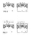
- phosphorus atoms is of the order of 1020 atoms/cm3; - diffusion of the doping impurities into polycrystalline silicon layer 6 and growth of a thin silicon dioxide layer 7, several tens nm thick by exposure in an oxidizing environment at a temperature of ca. 1 000° C (this silicon dioxide layer grown on polycrystalline silicon facilitates the subsequent operation); - formation, by photolitographic operations known from the prior art, of a photoresist mask 8, which protects a portion 9 of silicon dioxide layer 7. This mask limits a fixed gate area of the IGFET on region 30 of the substrate intended for the channel function of the transistor.
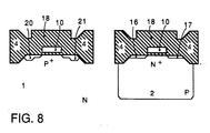
- This etching does not uncover portion 10 of polycrystalline silicon, since it is covered with a much thicker oxide; portion 10 of polycrystalline silicon which forms the gate electrode of the IGFET is thus completely surrounded by silicon dioxide ( Figure 5); the thickness of field oxide 4 does not undergo a significant reduction; - ion implantation of N-type doping impurities, e.g., arsenic (As) in regions 16 and 17 underlying the areas of the substrate uncovered by the previous etching: this operation results in the formation of the n+ source and drain regions of the transistor with an N channel.
- N-type doping impurities e.g., arsenic (As)
- the energy of implantation must be low in order to have a modest penetration of the doping agent into silicon; the dose of implanted doping impurities is very high, around 5 ⁇ 1015/cm2, in order to achieve high conductivity; - removal of the residual photoresist; - thermal treatment (annealing) at a moderate temperature in order to cause the substrate to recrystallize in the zone of implantation.
- the dose of implanted doping impurities is very high, around 5 ⁇ 1015 atoms/cm2, in order to achieve high conductivity; - removal of the residual photoresist; - exposure in an oxidising environment at low temperature (700-900° C), long enough to fully convert the non-monocrystalline silicon into an oxide.
- a part of the doping agent implanted in the preceding phase will be transferred into the underlying silicon, forming the source and drain regions 20 and 21 of the transistor; however, a part will remain trapped in the oxide. This must be taken into account when defining the implantation dose.
- the oxidation must be such as not to cause an excessive amount of the doping agent to diffuse into the substrate.
- precisely the presence of the polycrystalline silicon prevents an undesirable effect of increasing the diffusivity due to this oxidation.
- the polycrystalline silicon has the object of eliminating the channeling phenomenon, which is encountered when implanting boron into a monocrystalline substrate. In this way, the depth of the P+/N junction can be drastically reduced, giving rise to an increase of the length of the channel. The depth of the P+/N junction will be smaller where the implanted ions must traverse a greater thickness of polycrystalline silicon, i.e., at the edges of the gate region ( Figure 7).
- this causes the polycrystalline silicon layer to behave like a spacer between the gate region and the source and drain regions: in this way, the superposition between the gate region and the P+ regions can be reduced at will, thereby reducing the gate-source and gate-drain coupling capacities; this enables one to obtain high speeds of response of the transistor. Because the P+ regions extend very little below the gate, the effective length of the transistor increases and reduces the punch-through risk.
Landscapes
- Metal-Oxide And Bipolar Metal-Oxide Semiconductor Integrated Circuits (AREA)
- Insulated Gate Type Field-Effect Transistor (AREA)
- Thin Film Transistor (AREA)
Applications Claiming Priority (2)
| Application Number | Priority Date | Filing Date | Title |
|---|---|---|---|
| IT22182/86A IT1197523B (it) | 1986-10-30 | 1986-10-30 | Processo per la fabbricazione di transistori ad effetto di campo a "gate" isolata con giunzioni aventi profondita' estremamente ridotta |
| IT2218286 | 1986-10-30 |
Publications (2)
| Publication Number | Publication Date |
|---|---|
| EP0265958A2 true EP0265958A2 (fr) | 1988-05-04 |
| EP0265958A3 EP0265958A3 (fr) | 1989-09-27 |
Family
ID=11192707
Family Applications (1)
| Application Number | Title | Priority Date | Filing Date |
|---|---|---|---|
| EP87115933A Withdrawn EP0265958A3 (fr) | 1986-10-30 | 1987-10-29 | Procédé pour faire des transistors à effet de champ à porte isolée |
Country Status (3)
| Country | Link |
|---|---|
| EP (1) | EP0265958A3 (fr) |
| JP (1) | JPS63117459A (fr) |
| IT (1) | IT1197523B (fr) |
Cited By (1)
| Publication number | Priority date | Publication date | Assignee | Title |
|---|---|---|---|---|
| EP0631306A1 (fr) * | 1993-06-23 | 1994-12-28 | Siemens Aktiengesellschaft | Procédé de fabrication d'une région d'isolation dans un substrat pour la technologie de puissance intélligente |
Families Citing this family (2)
| Publication number | Priority date | Publication date | Assignee | Title |
|---|---|---|---|---|
| JP2002368012A (ja) * | 2001-06-06 | 2002-12-20 | Rohm Co Ltd | 不純物拡散層の形成方法 |
| JP4933957B2 (ja) * | 2007-05-18 | 2012-05-16 | 住友ゴム工業株式会社 | スポンジたわし |
Family Cites Families (5)
| Publication number | Priority date | Publication date | Assignee | Title |
|---|---|---|---|---|
| JPS56160034A (en) * | 1980-05-14 | 1981-12-09 | Fujitsu Ltd | Impurity diffusion |
| CA1198226A (fr) * | 1982-06-01 | 1985-12-17 | Eliezer Kinsbron | Methode de fabrication d'un dispositif semiconducteur |
| JPS6063961A (ja) * | 1983-08-30 | 1985-04-12 | Fujitsu Ltd | 半導体装置の製造方法 |
| IT1213192B (it) * | 1984-07-19 | 1989-12-14 | Ates Componenti Elettron | Processo per la fabbricazione di transistori ad effetto di campo agate isolato (igfet) ad elevata velocita' di risposta in circuiti integrati ad alta densita'. |
| IT1213234B (it) * | 1984-10-25 | 1989-12-14 | Sgs Thomson Microelectronics | Procedimento perfezionato per la fabbricazione di dispositivi a semiconduttore dmos. |
-
1986
- 1986-10-30 IT IT22182/86A patent/IT1197523B/it active
-
1987
- 1987-10-29 EP EP87115933A patent/EP0265958A3/fr not_active Withdrawn
- 1987-10-30 JP JP62273600A patent/JPS63117459A/ja active Pending
Cited By (2)
| Publication number | Priority date | Publication date | Assignee | Title |
|---|---|---|---|---|
| EP0631306A1 (fr) * | 1993-06-23 | 1994-12-28 | Siemens Aktiengesellschaft | Procédé de fabrication d'une région d'isolation dans un substrat pour la technologie de puissance intélligente |
| US5700712A (en) * | 1993-06-23 | 1997-12-23 | Siemens Aktiengesellschaft | Method for manufacturing an insulating trench in an SOI substrate for smartpower technologies |
Also Published As
| Publication number | Publication date |
|---|---|
| EP0265958A3 (fr) | 1989-09-27 |
| IT8622182A0 (it) | 1986-10-30 |
| IT1197523B (it) | 1988-11-30 |
| JPS63117459A (ja) | 1988-05-21 |
Similar Documents
| Publication | Publication Date | Title |
|---|---|---|
| JP2663402B2 (ja) | Cmos集積回路デバイスの製造方法 | |
| US5766991A (en) | CMOS process utilizing disposable silicon nitride spacers for making lightly doped drain | |
| KR970000535B1 (ko) | Mos 전계효과 트랜지스터 및 그 회로 제조방법 | |
| EP0465045B1 (fr) | Procédé pour fabriquer des transistors à effet de champ pour circuits intégrés | |
| KR20010110769A (ko) | 반도체 디바이스 및 그 제조 방법 | |
| US5872049A (en) | Nitrogenated gate structure for improved transistor performance and method for making same | |
| EP0459398B1 (fr) | Méthode de fabrication du canal d'un dispositif semi-conducteur MOS | |
| US5106768A (en) | Method for the manufacture of CMOS FET by P+ maskless technique | |
| JP3492973B2 (ja) | 半導体装置の製造方法 | |
| EP0265958A2 (fr) | Procédé pour faire des transistors à effet de champ à porte isolée | |
| EP0809286B1 (fr) | Procédé de manufacture de dispositifs semi-conducteurs ayant des régions profondes variées | |
| KR0146525B1 (ko) | 반도체 소자의 트랜지스터 제조방법 | |
| JPH08255903A (ja) | 半導体装置及びその製造方法 | |
| US20040132240A1 (en) | Method of manufacturing CMOS semiconductor device | |
| JPS63283155A (ja) | 半導体装置およびその製造方法 | |
| JPH03297148A (ja) | 半導体装置の製造方法 | |
| JPH0629315A (ja) | 半導体装置及び半導体装置の製造方法 | |
| KR0137549B1 (ko) | 모스 트랜지스터 접합 형성 방법 | |
| JPH09232444A (ja) | 半導体集積回路装置およびその製造方法 | |
| KR940001398B1 (ko) | Mosfet 제조방법 | |
| JPH0590574A (ja) | 半導体装置 | |
| JPH04346263A (ja) | Bi−CMOS半導体装置の製造方法 | |
| JPS63217655A (ja) | 半導体装置の製造方法 | |
| JPH04276655A (ja) | Cmos半導体装置の製造方法 | |
| JPH05226595A (ja) | 相補型misトランジスタ装置 |
Legal Events
| Date | Code | Title | Description |
|---|---|---|---|
| PUAI | Public reference made under article 153(3) epc to a published international application that has entered the european phase |
Free format text: ORIGINAL CODE: 0009012 |
|
| AK | Designated contracting states |
Kind code of ref document: A2 Designated state(s): DE FR GB NL SE |
|
| PUAL | Search report despatched |
Free format text: ORIGINAL CODE: 0009013 |
|
| AK | Designated contracting states |
Kind code of ref document: A3 Designated state(s): DE FR GB NL SE |
|
| STAA | Information on the status of an ep patent application or granted ep patent |
Free format text: STATUS: THE APPLICATION IS DEEMED TO BE WITHDRAWN |
|
| 18D | Application deemed to be withdrawn |
Effective date: 19900328 |
|
| RIN1 | Information on inventor provided before grant (corrected) |
Inventor name: MEDA, LAURA, DR. Inventor name: POLIGNANO, MARIA LUISA, DR. |