EP0301603B1 - Ausgangsschaltung einer integrierten Halbleiterschaltungsanordnung - Google Patents
Ausgangsschaltung einer integrierten Halbleiterschaltungsanordnung Download PDFInfo
- Publication number
- EP0301603B1 EP0301603B1 EP88112482A EP88112482A EP0301603B1 EP 0301603 B1 EP0301603 B1 EP 0301603B1 EP 88112482 A EP88112482 A EP 88112482A EP 88112482 A EP88112482 A EP 88112482A EP 0301603 B1 EP0301603 B1 EP 0301603B1
- Authority
- EP
- European Patent Office
- Prior art keywords
- output
- voltage
- transistor
- semiconductor integrated
- output transistor
- Prior art date
- Legal status (The legal status is an assumption and is not a legal conclusion. Google has not performed a legal analysis and makes no representation as to the accuracy of the status listed.)
- Expired - Lifetime
Links
- 239000004065 semiconductor Substances 0.000 title claims description 33
- 238000007599 discharging Methods 0.000 claims description 26
- 239000008186 active pharmaceutical agent Substances 0.000 claims description 12
- 230000004044 response Effects 0.000 claims description 11
- 230000008859 change Effects 0.000 claims description 8
- 230000009467 reduction Effects 0.000 claims description 7
- 230000006870 function Effects 0.000 claims description 6
- 230000004913 activation Effects 0.000 claims 2
- 238000001514 detection method Methods 0.000 description 17
- 238000010276 construction Methods 0.000 description 16
- 238000010586 diagram Methods 0.000 description 13
- 239000003990 capacitor Substances 0.000 description 4
- 238000000034 method Methods 0.000 description 4
- 230000000694 effects Effects 0.000 description 3
- 230000008569 process Effects 0.000 description 3
- 230000003111 delayed effect Effects 0.000 description 2
- 230000000630 rising effect Effects 0.000 description 2
- 230000001629 suppression Effects 0.000 description 2
- 230000003213 activating effect Effects 0.000 description 1
- 230000005540 biological transmission Effects 0.000 description 1
- 238000007796 conventional method Methods 0.000 description 1
- 238000012886 linear function Methods 0.000 description 1
- 230000003071 parasitic effect Effects 0.000 description 1
- 230000002035 prolonged effect Effects 0.000 description 1
Images


Classifications
-
- G—PHYSICS
- G11—INFORMATION STORAGE
- G11C—STATIC STORES
- G11C7/00—Arrangements for writing information into, or reading information out from, a digital store
- G11C7/10—Input/output [I/O] data interface arrangements, e.g. I/O data control circuits, I/O data buffers
- G11C7/1051—Data output circuits, e.g. read-out amplifiers, data output buffers, data output registers, data output level conversion circuits
- G11C7/1057—Data output buffers, e.g. comprising level conversion circuits, circuits for adapting load
-
- G—PHYSICS
- G11—INFORMATION STORAGE
- G11C—STATIC STORES
- G11C7/00—Arrangements for writing information into, or reading information out from, a digital store
-
- G—PHYSICS
- G11—INFORMATION STORAGE
- G11C—STATIC STORES
- G11C7/00—Arrangements for writing information into, or reading information out from, a digital store
- G11C7/10—Input/output [I/O] data interface arrangements, e.g. I/O data control circuits, I/O data buffers
- G11C7/1051—Data output circuits, e.g. read-out amplifiers, data output buffers, data output registers, data output level conversion circuits
-
- G—PHYSICS
- G11—INFORMATION STORAGE
- G11C—STATIC STORES
- G11C7/00—Arrangements for writing information into, or reading information out from, a digital store
- G11C7/22—Read-write [R-W] timing or clocking circuits; Read-write [R-W] control signal generators or management
-
- H—ELECTRICITY
- H03—ELECTRONIC CIRCUITRY
- H03K—PULSE TECHNIQUE
- H03K19/00—Logic circuits, i.e. having at least two inputs acting on one output; Inverting circuits
- H03K19/003—Modifications for increasing the reliability for protection
- H03K19/00346—Modifications for eliminating interference or parasitic voltages or currents
- H03K19/00361—Modifications for eliminating interference or parasitic voltages or currents in field effect transistor circuits
Definitions
- This invention relates to a semiconductor integrated circuit with an output circuit for externally outputting a signal or data, and more particularly to a semiconductor integrated circuit in which a signal or data output speed can be controlled in accordance with a control signal.
- a signal or data is externally supplied via an output circuit which is generally called an output buffer circuit.
- a semiconductor memory device is designed to meet the application thereof and at the same time to attain a preset readout speed in a condition that a load capacitance of approx. 100 pF is connected to the data output terminal.
- address access time t ACC from a time that the address signal starts to vary to a time that data is read out is set to 150 ns at maximum.
- time t OE from a time that output enable signal OE is activated to a time that output data is determined is set to approx. 70 ns at maximum.
- the output circuit includes a buffer amplifier section for directly driving the load, and a pre-amplifier section for driving the buffer amplifier section.
- transistors constituting the pre-amplifier section or transistors constituting the buffer amplifier section are each formed to have a small channel width in the prior art.
- the channel width of the transistor of the pre-amplifier section is set to be small, the current driving ability of the transistor becomes small, thereby causing the potential of a signal supplied to the gate of the transistor of the buffer amplifier section to rise or fall slowly. Therefore, current flowing in the buffer amplifier section will not vary abruptly, suppressing the noise generation due to the fluctuation in the power source voltage. Also, when the transistor of the buffer amplifier section has a small channel width, a small amount of current flows in the buffer amplifier section. This suppresses the generation of noise due to the fluctuation in the power source voltage, thereby preventing an erroneous circuit operation of the IC. However, with these methods, the operation speed or the data readout speed will be lowered.
- Prior art document EP-A-0 164 615 discloses a circuit for adjusting the rise and fall times of an output signal of a driver circuit to correspond to reference rise and fall times by using a feedback circuit acting on the gates of output MOS transistors.
- the present invention provides a semiconductor integrated circuit as specified in claim 1 or 2.
- control circuit is operated to charge or discharge the preset node of the data output circuit for a preset period of time after the control signal has changed in level. Therefore, the preset node can be rapidly charged or discharged, permitting data to be read out at a high speed.
- the address input signal is supplied to the row decoder and column decoder via the address buffer.
- the row decoder functions to select a memory cell, and the readout data from the selected memory cell is supplied to the column line.
- the readout data supplied to the column line is further supplied to the data sensing circuit via the column gate which is selectively controlled by means of the column decoder. Data sensed by the data sensing circuit is supplied to the exterior by means of the output circuit.
- address access time t ACC is the sum of delay time in such circuit blocks, so data transmission time in the output circuit section occupies only a small portion of address access time t ACC . Therefore, address access time t ACC will not be influenced even if the charging and discharging speeds in the output buffer section of the output circuit are low.
- output buffer enable signal OE is supplied to the output circuit only via the OE buffer circuit, substantially all portion of time t OE is occupied by the delay time in the output circuit. Thus, the charging and discharging speeds in the output circuit become one of the most important factors for determining time t OE .
- Fig. 1 is a block diagram showing the entire construction of a semiconductor memory device (programmable read only memory) according to one embodiment of this invention.
- Chip enable control circuit 11 generates internal chip enable signals CE* and CE* in response to chip enable signal CE .
- Output enable/program control circuit 12 generates internal output enable signals OE* and OE* and internal program signal PGM* in response to externally supplied output enable signal OE and program signal PGM .
- External address signal Add and internal chip enable signals CE* and CE* are input to address buffer 13 which outputs internal address signal Add* when signals CE* and CE* are activated.
- An internal address signal Add* output from address buffer 13 is supplied to row decoder 14 and column decoder 15. Internal chip enable signals CE* and CE* are also supplied to row decoder 14 and column decoder 15. Row decoder 14 is operated when chip enable signals CE* and CE* are activated, and selectively drives row line 17 in memory cell array 16 in response to internal address Add*.
- data is read out from a plurality of memory cells (not shown) connected to row line 17. Data thus read out is input to column gate circuit 19 via column line 18.
- Column decoder 15 is operated when chip enable signals CE* and CE* are activated, and controls the operation of column gate circuit 19 in response to internal address Add*. As a result of the control operation, column gate circuit 19 will select n bits out of m-bit data (m > n) read out from memory cell array 16. Then, n-bit data selected by column gate circuit 19 is input to data detection circuit 20.
- Data detection circuit 20 is connected to chip enable signals CE* and CE* and reference voltage Vref generated from reference potential generating circuit 21. Data detection circuit 20 is operated when signals CE* and CE* are activated, and determines data by comparing the data from column gate circuit 19 with reference voltage Vref. Data thus determined is input to output circuit 22.
- Internal output enable signals OE* and OE* and internal program signal PGM* from output enable/program control circuit 12 and signals CE* and CE* from chip enable control circuit 11 are supplied to output control circuit 23.
- Output control circuit 23 detects variation in level of external output enable signal OE based on internal output enable signals OE* and OE* , and produces pulses P and P with a preset pulse width. Pulse signals P and P are supplied together with internal output enable signals OE* and OE* to output circuit 22.
- Output circuit 22 is operated in response to pulse signals P and P and internal output enable signals OE* and OE* to supply data Dout of plural bits corresponding to detection data from data detection circuit 20 to the outside of the chip.
- the memory device in this embodiment is similar to the conventional memory device except that output control circuit 23 is used and output circuit 22 is controlled by pulse signals P and P generated from output control circuit 23 in addition to internal output enable signals OE* and OE* .
- Fig. 2 is a circuit diagram showing the construction of part of output circuit 22 included in the memory device shown in Fig. 1 which processes one-bit data.
- One-bit data DS detected by data detection circuit 20 is supplied to CMOS inverter 33 which is constituted by P-channel MOS transistor 31 and N-channel MOS transistor 32 having current paths connected in series between power source terminals Vcc and Vss (or ground).
- An output of inverter 33 is supplied to CMOS inverter 36 which is constituted by P-channel MOS transistor 34 and N-channel MOS transistor 35 having current paths connected in series between power source terminals Vcc and Vss.
- the current paths of P-channel MOS transistor 37 and two N-channel MOS transistors 38 and 39 are connected in series between power source terminals Vcc and Vss.
- the gates of P-channel MOS transistor 37 and N-channel MOS transistor 38 are connected to receive an output of inverter 36, and the gate of N-channel MOS transistor 39 is connected to receive internal output enable signal OE*.
- the current paths of two N-channel MOS transistors 41 and 42 are connected in series between power source terminal Vss and connection node 40 between P-channel MOS transistor 37 and N-channel MOS transistor 38.
- the gates of N-channel MOS transistors 41 and 42 are connected to receive an output of inverter 36 and pulse signal P, respectively.
- the current path of P-channel MOS transistor 43 whose gate is connected to receive internal output enable signal OE* is connected between node 40 and power source terminal Vcc.
- the current paths of two P-channel MOS transistors 44 and 45 and N-channel MOS transistor 46 are connected in series between power source terminals Vcc and Vss.
- the gates of P-channel MOS transistor 45 and N-channel MOS transistor 46 are connected to receive an output of inverter 36, and the gate of P-channel MOS transistor 44 is connected to receive internal output enable signal OE* .
- the current paths of two P-channel MOS transistors 48 and 49 are connected in series between power source terminal Vcc and connection node 47 between P-channel MOS transistor 45 and N-channel MOS transistor 46.
- the gates of P-channel MOS transistors 48 and 49 are connected to receive pulse signal P and an output of inverter 36, respectively.
- the current path of N-channel MOS transistor 50 whose gate is connected to receive internal output enable signal OE* is connected between node 47 and power source terminal Vss.
- P-channel MOS transistor 51 and N-channel MOS transistor 52 are connected in series between power source terminals Vcc and Vss.
- the gates of P-channel MOS transistor 51 and N-channel MOS transistor 52 are connected to nodes 40 and 47, respectively.
- data output terminal (or pad) 54 is connected to connection node 53 between transistors 51 and 52, and data Dout is supplied from terminal 54 to the exterior.
- Two inverters 33 and 36, and transistors 37 to 50 constitute pre-amplifier section PB, and other transistors 51 and 52 constitute buffer amplifier section BA.
- P-channel MOS transistor 51 and N-channel MOS transistor 52 provided at the buffer amplifier BA are formed to have a conductance larger than that of the other transistors.
- the operation mode of the PROM includes a programming mode in which data is programmed and a readout mode in which data is read out.
- the readout mode includes three modes: an output disable mode in which data is read out from a memory cell array in response to an address signal but is not supplied to the exterior, a standby mode in which data is not read out and an active mode in which readout data is supplied to the exterior.
- an output of inverter 36 is supplied to the gate of P-channel MOS transistor 51 via a CMOS inverter constituted by P-channel MOS transistor 37 and N-channel MOS transistor 38, and to the gate of N-channel MOS transistor 52 via CMOS inverter constituted by P-channel MOS transistor 45 and N-channel MOS transistor 46.
- nodes 40 and 47 are set to "1" level.
- N-channel MOS transistor 52 is turned on and data Dout of node 53 is inverted to "0" level.
- node 47 is charged via the current paths of P-channel MOS transistors 44 and 45 at a relatively low charging speed, and therefore data Dout falls slowly to "0" level.
- N-channel MOS transistor 39 is turned on and P-channel MOS transistor 43 is turned off, causing node 40 to be discharged via the serial current paths of N-channel MOS transistors 38 and 39.
- pulse signals P and P from control circuit 23 are respectively set at "1" and "0" levels for a preset period of time.
- signal P is at "1" level
- N-channel MOS transistor 42 is turned on. Since, at this time, N-channel MOS transistor 41 is set in the conductive state, node 40 will be discharged via the current paths of N-channel MOS transistors 41 and 42 in addition to those of N-channel MOS transistors 38 and 39. Therefore, the discharging speed at which node 40 is discharged to "0" level is enhanced in comparison with the case of the active mode. As a result, P-channel MOS transistor 51 is rapidly turned on, causing data Dout to rise rapidly to "1" level.
- P-channel MOS transistor 48 is turned on. Since, in this case, P-channel MOS transistor 49 is set in the conductive state, node 47 is charged via the current paths of P-channel MOS transistors 48 and 49 in addition to the case of P-channel MOS transistors 44 and 45. Therefore, the charging speed at which node 47 is charged to "1" level is enhanced in comparison with the case of the active mode. As a result, N-channel MOS transistor 52 is rapidly turned on, causing data Dout to fall rapidly to "0" level.
- data can be rapidly read out in the output disable mode in which high operation speed is required.
- address signal Add has been set and then a certain period of time has passed before signal OE is activated to supply data Dout to the exterior. Therefore, even if the power source voltage has varied due to noise generation, there is no possibility of the memory device being erroneously operated.
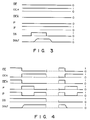
- Figs. 5 and 6 show the voltage waveforms at respective points in the memory device according to the above embodiment, Fig. 5 showing the case of the active mode and Fig. 6 showing the case of the output disable mode. Da shown in Figs. 5 and 6 is output data of column gate circuit 19. As is clearly understood from Figs. 5 and 6, output data Dout is rapidly rises to "1" level in the output disable mode than in the active mode.
- Fig. 7 shows the waveforms of the signals which are generated in the circuit when the potential of node 40 and the potential of output signal Dout are rapidly lowered and raised, respectively.
- Data detection circuit 20 compares the data Da read from the memory cells, with the reference potential Vref, thus determining whether the data DS is at the "H" or "L” level.
- the output circuit operates at high speed, the potential of node 40 starts falling, and the output node 53 is therefore charged, before the potential of the data Da deviates from the reference voltage Vref.
- a large current flows from the output buffer to the output terminal, and both the power source potential and the ground potential fluctuate. Consequently, noise is generated.
- the noise inverts the relationship in level between the reference potential Vref and the potential of data Da, which are not sufficiently different from each other.
- the data Da becomes erroneous. More specifically, the potential of this data rises above the reference potential Vref since the noise is superposed on the data Da when ⁇ VD is small immediately the potential of the data Da falls below potential Vref during the discharging of data Da.
- the sense amplifier detects this potential rise of data Da. Nonetheless, the difference ⁇ VD between potential Vref and the potential of data Da remains sufficiently great since both the reference potential Vref and that of data Da are fixed during period t OE or period t PGM , as is illustrated in Fig. 6.
- Fig. 8 is a circuit diagram showing the detail construction of output enable/program control circuit 12 and output control circuit 23 in the memory device of the above embodiment.
- Pad or terminal 61 is connected to receive signal OE .
- P-channel MOS transistor 62 is turned on, N-channel MOS transistor 63 is turned off, N-channel MOS transistor 64 is turned on and P-channel MOS transistor 65 is turned off in output enable/program control circuit 12. Therefore, signal OE supplied to terminal 61 is supplied as output enable OE* via CMOS inverters 66 and 67, and output as internal output enable signal OE* via CMOS inverter 69.
- an output signal of inverter 68 in circuit 12 is supplied to CMOS NAND circuit 80 including P- and N-channel MOS transistors via CMOS NAND circuit 79 which functions as an inverter. Further, an output signal of NAND circuit 79 is supplied to CMOS NAND circuit 80 via CMOS inverter 81, signal delay circuit 82 including P- and N-channel MOS transistors, CMOS inverter 83, signal delay circuit 84 with the same construction as signal delay circuit 82 and three CMOS inverters 85 to 87. A signal on output node 88 of NAND circuit 79 and that on output node 89 of inverter 87 are generated with a certain time delay from each other and are set in the inverted logic states.
- a pulse signal which is set to "0" level only when signals on nodes 88 and 89 are both set at "1" level is generated from output node 90 of NAND circuit 80.
- the pulse signal is supplied as pulse signal P via CMOS inverter 91 and as pulse signal P via CMOS inverters 91 and 92.
- Fig. 9 is a circuit diagram showing the construction of part of output circuit 22 which is provided in the memory device shown in Fig. 1 and which processes one bit of data.
- This output circuit has two output sections PB1 and PB2, both corresponding to pre-amplifier section PB shown in Fig. 2.
- the output signal of the PBO which is equivalent to the input of pre-amplifier section PB, is supplied to output sections PB1 and PB2.
- the outputs of these sections PB1 and PB2 are input to two buffer amplifier sections BA1 and BA2, respectively.
- Pre-amplifier sections PB1 and PB2 are formed to have the construction obtained by omitting N-channel MOS transistors 41 and 42 and P-channel MOS transistors 48 and 49 from pre-amplifier section BA shown in Fig. 2.
- One of pre-amplifier section BA1 is connected to receive signals OE*1 and OE*1 instead of internal output enable signals OE* and OE*
- the other pre-amplifier section PB2 is connected to receive signals OE*2 and OE*2 instead of internal output enable signals OE* and OE* .
- Output nodes 53 of buffer amplifier sections BA1 and BA2 are connected to terminal 54. Two sets of signals OE*1 and OE*1 and signals OE*2 and OE*2 are generated at different timings from output control circuit 23.
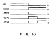
- Internal output enable signals OE*2 and OE*2 are set at "1" and "0" levels respectively for a preset period of time after signal OE has been activated.
- buffer amplifier section BA2 is operated for a preset period of time after signal OE has been activated.
- signals OE*2 and OE*2 are set to "1" and "0" levels, respectively.
- the operation speed of charging or discharging node 54 is enhanced and data can be read out at a higher speed in a period of time in which buffer amplifier section BA2 than in a case in which only buffer amplifier section BA1 is operated.
- the number of stages of the buffer amplifier sections is increased and therefore the output circuit becomes easily influenced by power source noise in comparison with the output circuit shown in Fig. 2.
- output section PB1 and buffer amplifier section BA1 have a response speed different from that of output section PB2 and buffer amplifier section BA2.
- Output section PB1 and buffer amplifier section BA1 have the same response speed when transistors 42 and 48 (both shown in Fig. 2) are off. Therefore, nodes 40 and 47 of buffer amplifier section BA1 are slowly discharged and charged, respectively, whereas nodes 40 and 47 of buffer amplifier section BA2 are quickly discharged.
- the output terminal which has been charged to the power source potential is discharged.
- the output terminal is discharged. Therefore, di/dt is influenced by the current-voltage characteristic of the transistor.
- the output buffer transistor is operated in the saturation region until the drain voltage becomes lower than the gate voltage by the threshold voltage.
- gate voltage VG starts to rise.
- gate voltage VG rises linearly with respect to time.
- the rate of change in current with time can be obtained by differentiating equation (4) with respect to time t, and dID/dt can be obtained as follows:
- the rate of change in current dID/dt varies in proportion to the square of ⁇ X which is the rising inclination of the gate voltage and varies in proportion to channel width W of the transistor.
- the rate of change in current di/dt at the data output time can be more effectively reduced by making gentle the rising inclination of the gate voltage of the transistor to be turned on as shown in Fig. 2 than by reducing the channel width of the transistor to be turned on.
- the potential of the output terminal is gradually discharged, the drain voltage of the output buffer transistor is gradually lowered and the transistor is operated in the triode operation mode.
- the voltage-current characteristic of the MOS transistor operation in the triode operation mode can be approximately expressed in the form of linear function which is attained by resistance R.
- the power source voltage will fluctuate in a negative direction.
- the resistance of the MOS transistor becomes larger as the channel width thereof is set to be smaller. That is, in the discharging operation in the triode operation mode after the gate voltage has been raised to the power source voltage, fluctuation in the power source voltage can be suppressed to a small value if the channel width is set to be small. Further, as described above, the effects can be obtained in proportion to the square of the channel width.
- the conduction resistance of the MOS transistor is determined by the channel width, and at the same time, depends on the gate voltage thereof. That is, the conduction resistance becomes smaller as the gate voltage becomes higher.
- Fig. 11 is a circuit diagram showing the circuit which is constituted by taking the above effect into consideration so as to improve the circuit of Fig. 2.
- voltage V1 is used to obtain a voltage lower than power source voltage Vcc by a preset voltage and voltage V2 is used to obtain a voltage higher than power source voltage Vss by a preset voltage.
- the rate of change in the gate voltage of the output buffer MOS transistor is reduced to improve di/dt.
- the gate voltage of the output buffer MOS transistor is set to be lower than Vcc or higher than Vss so as to increase the conduction resistance of the MOS transistor, thus improving di/dt.
- transistors 44 and 39 it is possible to provide V1 and V2 only in transistors 44 and 39. This is because transistors 42 and 48 are set in the nonconductive state in a period in which it is necessary to reduce di/dt and which ranges from the change of address in the state in which signal OE is set at "0" level to the data output time.
- Fig. 12 is a circuit diagram showing the circuit of Fig. 11 for generating voltages V1 and V2.
- Voltage V1 is generated by means of P-channel MOS transistor 101 and 102 whose gate and drain are connected together respectively
- voltage V2 is generated by means of N-channel MOS transistor 103 and 104 whose gate and drain are connected together respectively.
- a voltage which is lower than power source voltage Vcc by the threshold of the P-channel MOS transistor is supplied to MOS transistors 44 and 48, and a voltage which is higher than ground voltage Vss by the threshold voltage of the N-channel MOS transistor is supplied to MOS transistors 39 and 42.
- the output voltage is set to have a potential difference equal to the threshold voltage of the MOS transistor, but it is possible to adjust the potential difference according to required di/dt.
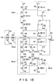
- Fig. 13 is a circuit diagram showing another construction of part of output circuit 22 which is provided in the memory device shown in Fig. 1 and which processes one bit of data.
- This output circuit has two output sections PB11 and PB12, both corresponding to pre-amplifier section PB shown in Fig. 2.
- the output signal of the PB10 which is equivalent to the input of pre-amplifier section PB, is supplied to output sections PB11 and PB12.
- the outputs of these sections PB11 and PB12 are input to two buffer amplifier sections BA11 and BA12, respectively.
- Each of buffer amplifier sections BA11 and BA12 is similar to buffer amplifier section BA of Fig.
- N-channel MOS transistor 52 of buffer amplifier section BA11 is connected to ground terminal Vss1 and N-channel MOS transistor 52 of buffer amplifier section BA12 is connected to ground terminal Vss2.
- Ground terminal Vss1 or Vss2 can also be used as another ground terminal Vss.
- data can be output at a high speed by operating BA11 and BA12 when signal OE is set at "0" level to derive out data.
- BA12 When address is changed to output new data with signal OE kept at “0" level, BA12 is operated.
- signals OE*2 and OE*2 are respectively set at "0" and “1" levels, and therefore variation in the gate voltage of output transistors 51 and 52 becomes gentle as in the case of the circuit shown in Fig. 2. That is, in the circuit of Fig. 13, in the saturation operation effected before data is output, the rate of change in the gate voltage is set small to suppress di/dt to a small value.
- the resistance thereof in the charging and discharging operations may be set to be large, suppressing di/dt to a small value. If, for example, data out put speeds attained when signal OE is set to "0" level are equal to each other in the circuits of Figs. 2 and 13, di/dt obtained in the triode operation mode when the address is changed with signal OE kept at "0" level will be more improved in the circuit of Fig. 13.
- two different power source terminals Vss are used to distribute the total amount of current flowing into the power source terminals Vss, and therefore, variation in the power source voltage can be suppressed to a smaller value in comparison with the case where only one power source terminal Vss is used, and erroneous operation can be effectively prevented. Further, if the power source for the circuit section in which noise may be generated is separated from the power source for the circuit section which may be easily influenced by noise, influence by noise can be reduced. Two or more power sources Vcc can be provided, as well as two or more power sources Vss.
- EPROMs erasable PROM
- a 1M-bit EPROM with 40 pins which is a sort of PROM includes two ground terminals.
- ground terminals of the buffer amplifier sections in the output circuit may be divided as shown in Fig. 13 so as to suppress noise.
- One of previously prepared two ground lines is connected to terminals Vss1 and Vss2 which are respectively connected to transistor 52 of buffer amplifier section BA11 and transistor 52 of buffer amplifier section BA12, and the other ground line is connected to terminal Vss of Fig. 13 terminal Vss outside the buffer amplifier section.
- output data can be supplied at a high speed when the high operation speed is required and the output data can be supplied at a low speed when it is required to suppress the noise occurrence.
- the first-type transistor which raises the potential of the output node toward power source Vcc level when it is turned on, or the second-type transistor which lowers the potential of the output node toward power source Vss level when it is turned on.
- the first-type transistor is used when the semiconductor integrated circuit includes a circuit which is more likely to make errors when power source voltage Vss changes than when power source voltage Vss changes.
- the second-type transistor is used when the semiconductor integrated circuit includes a circuit which is more likely to make errors when power source voltage Vss changes than when power source voltage Vcc changes.
- this invention is applied to the semiconductor memory device, but this invention can be applied to any semiconductor integrated circuit having an output circuit. With the use of this invention, it becomes possible to hold the high operation speed in selected circuit sections even if the average operation speed is lowered, and to enhance the reliability by selectively lowering the operation speed of circuit sections which are easily influenced by noise.
- the operation reliability of the circuit section which may be easily influenced by noise can be enhanced.
- This invention is not limited to the embodiment described above, and can be variously modified.
- a semiconductor integrated circuit can be provided in which the high operation speed and noise reduction in the output circuit can be attained at the same time.
Landscapes
- Physics & Mathematics (AREA)
- Engineering & Computer Science (AREA)
- Computer Hardware Design (AREA)
- Computing Systems (AREA)
- General Engineering & Computer Science (AREA)
- Mathematical Physics (AREA)
- Dram (AREA)
- Logic Circuits (AREA)
- Read Only Memory (AREA)
- Static Random-Access Memory (AREA)
- Electronic Switches (AREA)
Claims (13)
- Integrierte Halbleiterschaltung, die folgendes umfaßt:- eine Ausgangsschaltung (22), die einen Ausgangstransistor (51) enthält, wobei der Strompfad des Ausgangstransistors zwischen einer Versorgungsspannung (Vcc oder Vss) und einem Ausgangsknoten (53) liegt;- Vorlade-Einrichtungen (43 oder 50) zum Vorladen (auf Vcc) oder Entladen (auf Vss) der Steuerelektrode des Ausgangstransistors (51 oder 52) bevor Daten ausgegeben werden, so daß der Ausgangstransistor nichtleitend ist;- Einrichtungen (38, 39, oder 44, 45) zum bedingungsweisen Entladen oder Laden der Steuerelektrode des Ausgangstransistors (51 oder 52) gemäß einem internen Signal (DS) und als Antwort auf die Aktivierung eines Ausgabe-Freigabe-Signals (
OE ), so daß der Ausgangstransistor (51 oder 52) leitend gemacht wird, und- Steuereinrichtungen (41, 42, oder 48, 49), die die genannten Einrichtungen zum bedingungsweisen Vorladen oder Entladen beim Vorladen oder Entladen der Steuerelektrode des Ausgangstransistors (51 oder 52) für einen voreingestellten Zeitraum nach der Aktivierung des Ausgabe-Freigabe-Signals unterstützen und dadurch das Verringerungsmaß des Leitungswiderstandes des Ausgangstransistors (51 oder 52) für den voreingestellten Zeitraum erhöhen. - Integrierte Kalbleiterschaltung, die folgendes umfaßt:- eine Ausgangsschaltung (22), die einen ersten (51 oder 52) und einen zweiten (51' oder 52') Ausgangstransistor enthält, wobei die Strompfade der ersten und zweiten Transistoren zwischen einer Versorgungsspannung (Vcc oder Vss) und einem Ausgangsknoten (54) parallel geschaltet sind;- Vorlade-Einrichtungen (43 und 43' oder 50 und 50') zum Vorladen (auf Vcc) oder Entladen (auf Vss) der Steuerelektroden der ersten und zweiten Ausgangstransistoren bevor Daten ausgegeben werden, so daß die ersten und zweiten Ausgangstransistoren nichtleitend sind;- Einrichtungen (38, 39, oder 44, 45) zum bedingungsweisen Entladen oder Laden der Steuerelektrode des ersten Ausgangstransistors gemäß einem internen Signal (DS) und als Antwort auf die Aktivierung eines Ausgabe-Freigabe-Signals (
OE ), so daß der Ausgangstransistor bedingungsweise leitend gemacht wird; und- Einrichtungen (38', 39', oder 44', 45') zum bedingungsweisen Entladen oder Laden der Steuerelektrode des zweiten Ausgangstransistors gemäß dem internen Signal und für einen voreingestellten Zeitraum nach der Aktivierung des Ausgabe-Freigabe-Signals, so daß der zweite Ausgangstransistor für den voreingestellten Zeitraum leitend gemacht wird und dadurch den ersten Ausgangstransistor während des voreingestellten Zeitraums beim Schalten der Spannung am Ausgangsknoten unterstützt. - Integrierte Halbleiterschaltung gemäß Anspruch 1, dadurch gekennzeichnet, daß die Einrichtung zum Entladen oder Laden (38, 39) durch Anlegen einer Spannung (V2), die um einen vorbestimmten Wert höher als die Versorgungsspannung (Vss) ist, an die Steuerelektrode des genannten Ausgangstransistors (51) entlädt und die Einrichtung zum bedingungsweisen Entladen oder Laden (44, 45) durch Anlegen einer Spannung (V1), die um einen vorbestimmten Wert niedriger als die Versorgungsspannung (Vcc) ist, an die Steuerelektrode des Ausgangstransistors (52), lädt.
- Integrierte Halbleiterschaltung gemäß Anspruch 3, dadurch gekennzeichnet, daß die Steuereinrichtung (41, 42) durch Anlegen der Spannung (V2) an die Steuerelektrode des Ausgangstransistors (51) entlädt und die Steuereinrichtung (48, 49) durch Anlegen der Spannung (V1) an die Steuerelektrode des Ausgangstransistors (52) lädt.
- Integrierte Kalbleiterschaltung gemäß Anspruch 3, dadurch gekennzeichnet, daß die Spannung (V2) unter Verwendung einer Schwellenspannung des MOS-Transistors (103), der zwischen der bedingungsweisen Entlade- oder Ladeeinrichtung (38, 39) und der Versorgungsspannung (Vss) liegt und so angeschlossen ist, daß er als Diode arbeitet, erzeugt wird und die Spannung (V1) unter Verwendung einer Schwellenspannung des MOS-Transistors (101), der zwischen der bedingungsweisen Entlade- oder Ladeeinrichtung (44, 45) und der Versorgungsspannung (Vcc) liegt und so angeschlossen ist, daß er als Diode arbeitet, erzeugt wird.
- Integrierte Halbleiterschaltung gemäß Anspruch 4, dadurch gekennzeichnet, daß die Spannung (V2) unter Verwendung der Schwellenspannung eines MOS-Transistors (104), der zwischen der Steuereinrichtung (41, 42) und der Versorgungsspannung (Vss) liegt und so angeschlossen ist, daß er als Diode arbeitet, erzeugt wird und die Spannung (V1) unter Verwendung der Schwellenspannung des MOS-Transistors (102), der zwischen der Steuereinrichtung (48, 49) und der Versorgungsspannung (Vcc) liegt und so angeschlossen ist, daß er als Diode arbeitet, erzeugt wird.
- Integrierte Halbleiterschaltung gemäß Anspruch 2, gekennzeichnet durch Steuereinrichtungen (41, 42 oder 48, 49), die die bedingungsweise Entlade- oder Ladeeinrichtung beim Entladen oder Laden der Steuerelektrode des zweiten Ausgangstransistors (51' oder 52') für einen vorbestimmten Zeitraum nach der Aktivierung des Ausgabe-Freigabe-Signals unterstützen und dadurch das Verringerungsmaß des Bedingungs-widerstandes des zweiten Ausgangstransistors (51' oder 52') für den vorbestimmten Zeitraum erhöhen, wobei die ersten (52) und zweiten (52') Ausgangstransistoren mit verschiedenen Versorgungsspannungen (Vss1 und Vss2) verbunden sind.
- Integrierte Halbleiterschaltung gemäß Anspruch 1 oder 2, gekennzeichnet durch ein Feld von Speicherzellen (16), einen Reihen-Dekodierer (14) und einen Spalten-Dekodierer (15), die bei der Auswahl der Speicherzellen zusammenwirken, und eine Daten-Detektierschaltung (20), die die, in einer beliebigen Speicherzelle abgelegten, von den Reihen- und Spalten-Dekodierern (14 und 15) ausgewählten Daten (DS) ermittelt.
- Integrierte Halbleiterschaltung gemäß Anspruch 8, dadurch gekennzeichnet, daß das Steuersignal aus einem Ausgabe-Freigabesignal (
OE ) erzeugt wird, das von außen in die integrierte Halbleiterschaltung eingegeben wird. - Integrierte Halbleiterschaltung gemäß Anspruch 1, dadurch gekennzeichnet, daß die Steuereinrichtung einen Schalt-Transistor zum Laden oder Entladen der Gates der Ausgangstransistoren (51 und 52) enthält und das Verringerungsmaß durch Ändern der effektiven Kanalbreite des Schalt-Transistors verändert wird.
- Integrierte Halbleiterschaltung gemäß Anspruch 10, dadurch gekennzeichnet, daß der genannte Schalt-Transistor durch mehrere Schalt-Transistoren ersetzt wird und daß die Anzahl der Schalt-Transistoren, die gleichzeitig zum Laden oder Entladen des Gates des Ausgangstransistors (51 oder 52) benutzt werden, verändert wird, um so die effektive Kanalbreite zu verändern.
- Integrierte Halbleiterschaltung gemäß Anspruch 10 oder 11, dadurch gekennzeichnet, daß die Steuereinrichtung eine Vorrichtung zur Erzeugung von Impulssignalen einschließt, die ein Impulssignal (P und
P ) erzeugt, wenn ein Steuersignal zu einem hohen Pegel oder einem niedrigen Pegel wechselt und daß das Impulssignal (P undP ) zum Verändern der effektiven Kanalbreite benutzt wird. - Integrierte Halbleiterschaltung gemäß Anspruch 12, dadurch gekennzeichnet, daß die Steuereinrichtung den Ausgangstransistor (51 oder 52) ausschaltet, wenn das Steuersignal auf einem ersten logischen Pegel liegt, und den Ausgangstransistor (51 oder 52) einschaltet, wenn das Steuersignal vom ersten logischen Pegel aus ansteigt oder abfällt.
Applications Claiming Priority (2)
| Application Number | Priority Date | Filing Date | Title |
|---|---|---|---|
| JP19160287 | 1987-07-31 | ||
| JP191602/87 | 1987-07-31 |
Publications (3)
| Publication Number | Publication Date |
|---|---|
| EP0301603A2 EP0301603A2 (de) | 1989-02-01 |
| EP0301603A3 EP0301603A3 (de) | 1991-04-03 |
| EP0301603B1 true EP0301603B1 (de) | 1993-12-01 |
Family
ID=16277369
Family Applications (1)
| Application Number | Title | Priority Date | Filing Date |
|---|---|---|---|
| EP88112482A Expired - Lifetime EP0301603B1 (de) | 1987-07-31 | 1988-08-01 | Ausgangsschaltung einer integrierten Halbleiterschaltungsanordnung |
Country Status (5)
| Country | Link |
|---|---|
| US (1) | US4882507B1 (de) |
| EP (1) | EP0301603B1 (de) |
| JP (1) | JPH0799639B2 (de) |
| KR (1) | KR910009589B1 (de) |
| DE (1) | DE3885963T2 (de) |
Cited By (3)
| Publication number | Priority date | Publication date | Assignee | Title |
|---|---|---|---|---|
| FR2647581A1 (fr) * | 1989-05-26 | 1990-11-30 | Samsung Electronics Co Ltd | Circuit pour l'ajustement d'un niveau de tension de sortie de donnees dans un dispositif de memoire a semiconducteurs |
| EP0408032A3 (en) * | 1989-07-12 | 1992-08-05 | Kabushiki Kaisha Toshiba | Data output control circuit for semiconductor storage device |
| US5621342A (en) * | 1995-10-27 | 1997-04-15 | Philips Electronics North America Corporation | Low-power CMOS driver circuit capable of operating at high frequencies |
Families Citing this family (24)
| Publication number | Priority date | Publication date | Assignee | Title |
|---|---|---|---|---|
| JPH0777345B2 (ja) * | 1988-11-04 | 1995-08-16 | 三菱電機株式会社 | 半導体装置 |
| US5327392A (en) * | 1989-01-13 | 1994-07-05 | Kabushiki Kaisha Toshiba | Semiconductor integrated circuit capable of preventing occurrence of erroneous operation due to noise |
| JP2561167B2 (ja) * | 1989-04-18 | 1996-12-04 | 三菱電機株式会社 | バス回路 |
| JPH03185921A (ja) * | 1989-12-14 | 1991-08-13 | Toshiba Corp | 半導体集積回路 |
| US5019720A (en) * | 1990-03-12 | 1991-05-28 | Ncr Corporation | Integrated circuit driver for serial bus having output overvoltage protection |
| WO1991018394A1 (en) * | 1990-05-17 | 1991-11-28 | International Business Machines Corporation | Read/write/restore circuit for memory arrays |
| US5303191A (en) * | 1992-01-23 | 1994-04-12 | Motorola, Inc. | Memory with compensation for voltage, temperature, and processing variations |
| US5367645A (en) * | 1992-06-12 | 1994-11-22 | National Semiconductor Corporation | Modified interface for parallel access EPROM |
| US5430387A (en) * | 1992-09-16 | 1995-07-04 | International Business Machines Corporation | Transition-controlled off-chip driver |
| US5331220A (en) * | 1993-02-12 | 1994-07-19 | Xilinx, Inc. | Soft wakeup output buffer |
| US5557229A (en) * | 1994-05-16 | 1996-09-17 | Waferscale Integration, Inc. | Apparatus and method for producing an output signal from a memory array |
| GB2289808A (en) * | 1994-05-19 | 1995-11-29 | Motorola Gmbh | CMOS driver with programmable switching speed |
| JP3202481B2 (ja) * | 1994-05-30 | 2001-08-27 | 株式会社東芝 | 半導体集積回路 |
| KR0179859B1 (ko) * | 1995-11-24 | 1999-04-15 | 문정환 | 반도체 메모리의 출력 제어 회로 |
| EP0805453B1 (de) * | 1996-04-29 | 2004-01-02 | STMicroelectronics S.r.l. | Speicherarchitektur für flexibele Leseverwaltung, insbesondere für nichtflüchtige Speicher, mit Rauschunempfindlichkeitsmerkmalen, mit Anlageleistungsanpassung und mit optimiertem Durchfluss |
| US5917768A (en) * | 1997-04-24 | 1999-06-29 | Sgs-Thomson Microelectronics S.R.L. | Memory architecture for flexible reading management, particularly for non-volatile memories, having noise-immunity features, matching device performance, and having optimized throughout |
| JP3350411B2 (ja) * | 1997-09-24 | 2002-11-25 | 沖電気工業株式会社 | 半導体記憶装置の出力回路 |
| DE19949144C1 (de) * | 1999-10-12 | 2001-02-01 | Texas Instruments Deutschland | Digitale Treiberschaltung |
| US6166966A (en) * | 2000-01-07 | 2000-12-26 | Mitsubihsi Denki Kabushiki Kaisha | Semiconductor memory device including data output circuit capable of high speed data output |
| US6707715B2 (en) * | 2001-08-02 | 2004-03-16 | Stmicroelectronics, Inc. | Reference generator circuit and method for nonvolatile memory devices |
| ITVA20050002A1 (it) * | 2005-01-20 | 2006-07-21 | St Microelectronics Srl | Circuito di generazione di un segnale interno di abilitazione di un buffer di uscita di una memoria |
| KR100665905B1 (ko) * | 2005-09-29 | 2007-01-11 | 주식회사 하이닉스반도체 | 데이터 입력/출력 라인을 충전 또는 방전하는 래치를구비하는 메모리 장치 |
| US7656717B2 (en) * | 2005-09-29 | 2010-02-02 | Hynix Semiconductor, Inc. | Memory device having latch for charging or discharging data input/output line |
| JP4747023B2 (ja) * | 2006-04-27 | 2011-08-10 | Okiセミコンダクタ株式会社 | 半導体記憶装置 |
Citations (1)
| Publication number | Priority date | Publication date | Assignee | Title |
|---|---|---|---|---|
| US4061999A (en) * | 1975-12-29 | 1977-12-06 | Mostek Corporation | Dynamic random access memory system |
Family Cites Families (10)
| Publication number | Priority date | Publication date | Assignee | Title |
|---|---|---|---|---|
| JPS58161198A (ja) * | 1982-03-19 | 1983-09-24 | Ricoh Co Ltd | 半導体メモリ |
| JPS59181829A (ja) * | 1983-03-31 | 1984-10-16 | Toshiba Corp | 半導体素子の出力バツフア回路 |
| US4567378A (en) * | 1984-06-13 | 1986-01-28 | International Business Machines Corporation | Driver circuit for controlling signal rise and fall in field effect transistor processors |
| JPS61117785A (ja) * | 1984-11-14 | 1986-06-05 | Hitachi Ltd | 半導体集積回路装置 |
| JPS6231095A (ja) * | 1985-08-02 | 1987-02-10 | Nec Corp | 出力回路 |
| US4638187A (en) * | 1985-10-01 | 1987-01-20 | Vtc Incorporated | CMOS output buffer providing high drive current with minimum output signal distortion |
| JPS62150585A (ja) * | 1985-12-25 | 1987-07-04 | Nec Corp | Cmosメモリ回路 |
| JPS62220026A (ja) * | 1986-03-20 | 1987-09-28 | Toshiba Corp | 出力バツフア回路 |
| US4798979A (en) * | 1986-09-23 | 1989-01-17 | Honeywell Inc. | Schottky diode logic for E-mode FET/D-mode FET VLSI circuits |
| JPH06195792A (ja) * | 1992-12-22 | 1994-07-15 | Mitsubishi Electric Corp | 光磁気ディスク装置 |
-
1988
- 1988-07-29 US US07226307 patent/US4882507B1/en not_active Expired - Lifetime
- 1988-07-29 JP JP63190254A patent/JPH0799639B2/ja not_active Expired - Lifetime
- 1988-07-30 KR KR1019880009745A patent/KR910009589B1/ko not_active Expired
- 1988-08-01 EP EP88112482A patent/EP0301603B1/de not_active Expired - Lifetime
- 1988-08-01 DE DE88112482T patent/DE3885963T2/de not_active Expired - Lifetime
Patent Citations (1)
| Publication number | Priority date | Publication date | Assignee | Title |
|---|---|---|---|---|
| US4061999A (en) * | 1975-12-29 | 1977-12-06 | Mostek Corporation | Dynamic random access memory system |
Non-Patent Citations (1)
| Title |
|---|
| Electronics, 5 April 1984, pages 125-128, BATEMAN et al.: "C-MOS challenges bipolars in static-RAM race" * |
Cited By (3)
| Publication number | Priority date | Publication date | Assignee | Title |
|---|---|---|---|---|
| FR2647581A1 (fr) * | 1989-05-26 | 1990-11-30 | Samsung Electronics Co Ltd | Circuit pour l'ajustement d'un niveau de tension de sortie de donnees dans un dispositif de memoire a semiconducteurs |
| EP0408032A3 (en) * | 1989-07-12 | 1992-08-05 | Kabushiki Kaisha Toshiba | Data output control circuit for semiconductor storage device |
| US5621342A (en) * | 1995-10-27 | 1997-04-15 | Philips Electronics North America Corporation | Low-power CMOS driver circuit capable of operating at high frequencies |
Also Published As
| Publication number | Publication date |
|---|---|
| DE3885963D1 (de) | 1994-01-13 |
| EP0301603A3 (de) | 1991-04-03 |
| US4882507A (en) | 1989-11-21 |
| JPH0799639B2 (ja) | 1995-10-25 |
| DE3885963T2 (de) | 1994-05-05 |
| JPH01138814A (ja) | 1989-05-31 |
| KR910009589B1 (ko) | 1991-11-21 |
| EP0301603A2 (de) | 1989-02-01 |
| KR890002967A (ko) | 1989-04-12 |
| US4882507B1 (en) | 1993-03-16 |
Similar Documents
| Publication | Publication Date | Title |
|---|---|---|
| EP0301603B1 (de) | Ausgangsschaltung einer integrierten Halbleiterschaltungsanordnung | |
| US4918339A (en) | Data output circuit | |
| US5297104A (en) | Word line drive circuit of semiconductor memory device | |
| EP0301588A2 (de) | Halbleiterspeicheranordnung | |
| GB2184622A (en) | Output buffer having limited rate-of-change of output current | |
| US4985646A (en) | Output buffer circuit of semiconductor integrated circuit | |
| EP0347935B1 (de) | Halbleiterspeicheranordnung | |
| US5382847A (en) | Output buffer circuits including voltage compensation | |
| EP0186907A2 (de) | Nichtflüchtige Halbleiterspeicheranordnung mit Schreibeschaltung | |
| EP0573965B1 (de) | Halbleiteranordnung mit anschlusswählender Schaltung | |
| US5018107A (en) | Semiconductor memory device | |
| EP0280883B1 (de) | Halbleiter-Festwertspeichereinrichtung | |
| US20010043104A1 (en) | Delay circuit applied to semiconductor memory device having auto power-down function | |
| US4791614A (en) | Semiconductor memory device having erroneous write operation preventing function | |
| EP0194091B1 (de) | Programmierbare logische Schaltung mit begrenzten Leserströmen | |
| JPH0456400B2 (de) | ||
| US4019068A (en) | Low power output disable circuit for random access memory | |
| CA1115843A (en) | Dynamic precharge circuitry | |
| KR100267424B1 (ko) | 집적회로 | |
| US4926379A (en) | Data read circuit for use in semiconductor memory device | |
| JP3708561B2 (ja) | 出力回路 | |
| JPS6027118B2 (ja) | 半導体メモリ装置 | |
| JPH0512862A (ja) | 半導体集積回路装置 | |
| KR100317101B1 (ko) | 전원전압보다더높은전압을공급하는회로를구비한반도체회로 | |
| KR0150632B1 (ko) | 글리치 억제 회로 |
Legal Events
| Date | Code | Title | Description |
|---|---|---|---|
| PUAI | Public reference made under article 153(3) epc to a published international application that has entered the european phase |
Free format text: ORIGINAL CODE: 0009012 |
|
| 17P | Request for examination filed |
Effective date: 19880829 |
|
| AK | Designated contracting states |
Kind code of ref document: A2 Designated state(s): DE FR GB |
|
| PUAL | Search report despatched |
Free format text: ORIGINAL CODE: 0009013 |
|
| AK | Designated contracting states |
Kind code of ref document: A3 Designated state(s): DE FR GB |
|
| 16A | New documents despatched to applicant after publication of the search report | ||
| 17Q | First examination report despatched |
Effective date: 19920505 |
|
| GRAA | (expected) grant |
Free format text: ORIGINAL CODE: 0009210 |
|
| AK | Designated contracting states |
Kind code of ref document: B1 Designated state(s): DE FR GB |
|
| REF | Corresponds to: |
Ref document number: 3885963 Country of ref document: DE Date of ref document: 19940113 |
|
| ET | Fr: translation filed | ||
| PLBE | No opposition filed within time limit |
Free format text: ORIGINAL CODE: 0009261 |
|
| STAA | Information on the status of an ep patent application or granted ep patent |
Free format text: STATUS: NO OPPOSITION FILED WITHIN TIME LIMIT |
|
| 26N | No opposition filed | ||
| REG | Reference to a national code |
Ref country code: GB Ref legal event code: IF02 |
|
| PGFP | Annual fee paid to national office [announced via postgrant information from national office to epo] |
Ref country code: DE Payment date: 20070726 Year of fee payment: 20 |
|
| PGFP | Annual fee paid to national office [announced via postgrant information from national office to epo] |
Ref country code: GB Payment date: 20070801 Year of fee payment: 20 |
|
| PGFP | Annual fee paid to national office [announced via postgrant information from national office to epo] |
Ref country code: FR Payment date: 20070808 Year of fee payment: 20 |
|
| REG | Reference to a national code |
Ref country code: GB Ref legal event code: PE20 Expiry date: 20080731 |
|
| PG25 | Lapsed in a contracting state [announced via postgrant information from national office to epo] |
Ref country code: GB Free format text: LAPSE BECAUSE OF EXPIRATION OF PROTECTION Effective date: 20080731 |