EP0330176A2 - Couvercle de boîtier pour dispositifs à semiconducteur - Google Patents
Couvercle de boîtier pour dispositifs à semiconducteur Download PDFInfo
- Publication number
- EP0330176A2 EP0330176A2 EP89103085A EP89103085A EP0330176A2 EP 0330176 A2 EP0330176 A2 EP 0330176A2 EP 89103085 A EP89103085 A EP 89103085A EP 89103085 A EP89103085 A EP 89103085A EP 0330176 A2 EP0330176 A2 EP 0330176A2
- Authority
- EP
- European Patent Office
- Prior art keywords
- cover plate
- central portion
- package base
- portions
- set forth
- Prior art date
- Legal status (The legal status is an assumption and is not a legal conclusion. Google has not performed a legal analysis and makes no representation as to the accuracy of the status listed.)
- Granted
Links
Images

Classifications
-
- H—ELECTRICITY
- H10—SEMICONDUCTOR DEVICES; ELECTRIC SOLID-STATE DEVICES NOT OTHERWISE PROVIDED FOR
- H10W—GENERIC PACKAGES, INTERCONNECTIONS, CONNECTORS OR OTHER CONSTRUCTIONAL DETAILS OF DEVICES COVERED BY CLASS H10
- H10W76/00—Containers; Fillings or auxiliary members therefor; Seals
- H10W76/10—Containers or parts thereof
- H10W76/12—Containers or parts thereof characterised by their shape
-
- H—ELECTRICITY
- H10—SEMICONDUCTOR DEVICES; ELECTRIC SOLID-STATE DEVICES NOT OTHERWISE PROVIDED FOR
- H10W—GENERIC PACKAGES, INTERCONNECTIONS, CONNECTORS OR OTHER CONSTRUCTIONAL DETAILS OF DEVICES COVERED BY CLASS H10
- H10W76/00—Containers; Fillings or auxiliary members therefor; Seals
- H10W76/10—Containers or parts thereof
- H10W76/17—Containers or parts thereof characterised by their materials
Definitions
- the present invention relates to cover plates for semiconductor devices and more particularly to air tight cover plates especially adapted for use as peripheral casings of packages for semiconductor devices with a high data-packaging density such as LSIs.
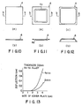
- FIG. 8 illustrates a conventional cover plate of this type.
- a semiconductor chip 2 is mounted in a center recess of a package base 1 and is electrically connected through bonding wires 3 to wiring leads.
- the upper portion of the semiconductor chip 2 is hermetically sealed by a cover plate 4 which is in the form of a flat plate as shown in FIG. 10 or is a flat plate which is locally formed with a furrow-shaped reinforcing rib 4a as shown in FIG. 11.
- the cover plate 4 is not in the form of one flat plate, but its whole peripheral portion is bent at a right angle so as to define a cap-shaped cover plate 4.
- an object of the present invention is to provide cover plates for semiconductor devices whose top portion is locally reinforced so that deflection resulting from the application of external force over the cover plate can be reduced to a minimum.
- the cover plate which covers a semiconductor chip mounted on a package base, according to the present invention, consists of a top wall portion in the form of a rectangle and side wall portions bent along the entire periphery of the rectangular top wall portion. Reinforcing portions are defined along the diagonal lines of the top wall portion.
- the reinforcing projected and recessed portions are defined along the diagonal lines of the metal cover plate, so that the bending strength at such reinforcing portions is increased, so that the deflection due to the application of the external force to the metal cover plate can be reduced to a minimum.
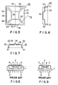
- FIGS. 1 to 7 a first and a second preferred embodiment of a cover plate for semiconductor devices in accordance with the present invention will be described in detail hereinbelow.
- a cover plate 10 is made of an Fe-Ni alloy and consists of an outermost flange portion 11, a side wall portion 12 extended substantially perpendicularly from the flange portion 11 and a center top portion 13 formed integrally with the side wall portion 12.
- the cover plate 10 covers the upper portion of the semiconductor chip 2 air-tightly, and the center top portion 13 is extended substantially in parallel with the upper surface of the semiconductor chip 2.
- the center top portion 13 consists of an outer region 14, an intermediate region 15 and an inner region 16.
- the outer region 14 is upwardly inclined at a relatively small gradient toward the center of the cover plate 10 while the intermediate region 15 is downwardly inclined inwardly, and the inner region 16 is a flat surface substantially in parallel with the package base.
- both the surfaces extended in the opposite directions from the diagonal line 17 intersect each other at an angle of intersection ⁇ 1 and define a roof-ridge-like portion and as best shown in FIG. 4, both of the surfaces 15 extended from the diagonal line 17 in opposite directions, respectively, interset each other at an angle of intersection ⁇ 2 and define a valley portion.
- the total of four roof-ridge-like portions and valley-like portions are defined along the diagonal line of the center top portion 13, so that the bending strength or the rigidity against bending force can be increased by the roof-ridge-like portions and the valley-like portions.
- the deflection of the metal cover plate 10 due to an external force applied thereto can be reduced to a minimum.
- a cover plate 20 made of an Fe-Ni alloy consists of an outermost peripheral flange portion 21, a side wall portion 22 extended substantially perpendicularly from the flange portion 21, and a central top portion 23 formed integrally with the upright side wall portion 22.
- the metal cover plate covers and hermetically seals the upper portion of a semiconductor chip 2.
- the top portion 23 consists of an outer region 24 and an inner region 25, and reinforcing ribs 28 are defined along the diagonal lines of the outer region 24. As best shown in FIG. 7, each rib 28 is semicircular in cross section and is extended upwardly so that level land portions 29 which are lower than the ribs 28 are defined between the adjacent ribs 28.
- the ribs 28 have been described as being extended upwardly, but it is understood that they may be extended downwardly or inwardly.
Landscapes
- Structures Or Materials For Encapsulating Or Coating Semiconductor Devices Or Solid State Devices (AREA)
Applications Claiming Priority (2)
| Application Number | Priority Date | Filing Date | Title |
|---|---|---|---|
| JP39035/88 | 1988-02-22 | ||
| JP63039035A JPH0793393B2 (ja) | 1988-02-22 | 1988-02-22 | 半導体装置の金属製シェル |
Publications (3)
| Publication Number | Publication Date |
|---|---|
| EP0330176A2 true EP0330176A2 (fr) | 1989-08-30 |
| EP0330176A3 EP0330176A3 (en) | 1990-10-31 |
| EP0330176B1 EP0330176B1 (fr) | 1993-08-04 |
Family
ID=12541856
Family Applications (1)
| Application Number | Title | Priority Date | Filing Date |
|---|---|---|---|
| EP89103085A Expired - Lifetime EP0330176B1 (fr) | 1988-02-22 | 1989-02-22 | Couvercle de boîtier pour dispositifs à semiconducteur |
Country Status (5)
| Country | Link |
|---|---|
| US (1) | US5096081A (fr) |
| EP (1) | EP0330176B1 (fr) |
| JP (1) | JPH0793393B2 (fr) |
| KR (1) | KR920006735B1 (fr) |
| DE (1) | DE68907943T2 (fr) |
Families Citing this family (2)
| Publication number | Priority date | Publication date | Assignee | Title |
|---|---|---|---|---|
| JP3462979B2 (ja) * | 1997-12-01 | 2003-11-05 | 株式会社東芝 | 半導体装置 |
| US9837333B1 (en) * | 2016-09-21 | 2017-12-05 | International Business Machines Corporation | Electronic package cover having underside rib |
Family Cites Families (14)
| Publication number | Priority date | Publication date | Assignee | Title |
|---|---|---|---|---|
| US3211503A (en) * | 1963-01-09 | 1965-10-12 | United Carr Inc | Container |
| US3327896A (en) * | 1965-06-04 | 1967-06-27 | Shell Oil Co | Stackable container |
| US4126758A (en) * | 1973-12-03 | 1978-11-21 | Raychem Corporation | Method for sealing integrated circuit components with heat recoverable cap and resulting package |
| CA1042116A (fr) * | 1973-12-03 | 1978-11-07 | John F. Krumme | Couvercle reformable a la chaleur |
| US4109818A (en) * | 1975-06-03 | 1978-08-29 | Semi-Alloys, Inc. | Hermetic sealing cover for a container for semiconductor devices |
| US4291815B1 (en) * | 1980-02-19 | 1998-09-29 | Semiconductor Packaging Materi | Ceramic lid assembly for hermetic sealing of a semiconductor chip |
| JPS5748250A (en) * | 1980-09-05 | 1982-03-19 | Nec Corp | Metal cap for semiconductor device |
| DE3040959A1 (de) * | 1980-10-30 | 1982-05-27 | Siemens AG, 1000 Berlin und 8000 München | Verpackung fuer elektrische bauelemente |
| JPS59201446A (ja) * | 1983-04-30 | 1984-11-15 | Toshiba Corp | 半導体装置及びその製造方法 |
| JPS60133741A (ja) * | 1983-12-21 | 1985-07-16 | Fujitsu Ltd | 半導体装置及びその製造方法 |
| JPS61204953A (ja) * | 1985-03-08 | 1986-09-11 | Sumitomo Metal Mining Co Ltd | ハ−メチツクシ−ルカバ−及びその製造方法 |
| JPS6226846A (ja) * | 1985-07-26 | 1987-02-04 | Nec Corp | 半導体装置封止用キヤツプ |
| US4640438A (en) * | 1986-03-17 | 1987-02-03 | Comienco Limited | Cover for semiconductor device packages |
| US4746583A (en) * | 1986-11-21 | 1988-05-24 | Indium Corporation | Ceramic combined cover |
-
1988
- 1988-02-22 JP JP63039035A patent/JPH0793393B2/ja not_active Expired - Lifetime
-
1989
- 1989-02-22 EP EP89103085A patent/EP0330176B1/fr not_active Expired - Lifetime
- 1989-02-22 US US07/313,555 patent/US5096081A/en not_active Expired - Lifetime
- 1989-02-22 DE DE89103085T patent/DE68907943T2/de not_active Expired - Fee Related
- 1989-02-22 KR KR1019890002087A patent/KR920006735B1/ko not_active Expired
Also Published As
| Publication number | Publication date |
|---|---|
| EP0330176A3 (en) | 1990-10-31 |
| EP0330176B1 (fr) | 1993-08-04 |
| JPH01214050A (ja) | 1989-08-28 |
| DE68907943D1 (de) | 1993-09-09 |
| KR890013752A (ko) | 1989-09-25 |
| JPH0793393B2 (ja) | 1995-10-09 |
| US5096081A (en) | 1992-03-17 |
| DE68907943T2 (de) | 1993-12-16 |
| KR920006735B1 (ko) | 1992-08-17 |
Similar Documents
| Publication | Publication Date | Title |
|---|---|---|
| EP0568781B1 (fr) | Structure d'empaquetage pour un ensemble détecteur de pression à semi-conducteurs | |
| US5072280A (en) | Resin sealed semiconductor device | |
| US6483181B2 (en) | Multi-chip package | |
| US6072700A (en) | Ball grid array package | |
| US7211883B2 (en) | Semiconductor chip package | |
| JPH0352255A (ja) | 回路基板及び半導体素子の実装方法 | |
| EP0330176A2 (fr) | Couvercle de boîtier pour dispositifs à semiconducteur | |
| JPS6348183B2 (fr) | ||
| US4661653A (en) | Package assembly for semiconductor device | |
| JP3290869B2 (ja) | 半導体装置 | |
| US6005293A (en) | Wire-bonded semiconductor device | |
| JP2530111B2 (ja) | 半導体装置の金属製シェル | |
| KR0124547Y1 (ko) | 멀티형 리드프레임을 이용한 반도체 장치 | |
| KR940008336B1 (ko) | 반도체 패키지 | |
| JP2584084B2 (ja) | 半導体装置用リードフレーム | |
| JPH05206307A (ja) | 半導体装置 | |
| JPS6234445Y2 (fr) | ||
| JPH03116767A (ja) | Icのパッケージ | |
| JPH01181450A (ja) | 樹脂封止型半導体装置 | |
| US4918512A (en) | Semiconductor package having an outwardly arced die cavity | |
| JPH03273667A (ja) | 樹脂封止型混成集積回路 | |
| JPS63104452A (ja) | 半導体装置の製造方法 | |
| JPH0254567A (ja) | 樹脂封止型半導体装置 | |
| JPS63211652A (ja) | 集積回路パツケ−ジ | |
| JPH0644106Y2 (ja) | リ−ドフレ−ム |
Legal Events
| Date | Code | Title | Description |
|---|---|---|---|
| PUAI | Public reference made under article 153(3) epc to a published international application that has entered the european phase |
Free format text: ORIGINAL CODE: 0009012 |
|
| 17P | Request for examination filed |
Effective date: 19890222 |
|
| AK | Designated contracting states |
Kind code of ref document: A2 Designated state(s): DE FR GB IT |
|
| RIN1 | Information on inventor provided before grant (corrected) |
Inventor name: SAKURAI, TOSHIHARU Inventor name: SHINDO, MASAMICHI Inventor name: IZAWA, NOBU Inventor name: TAGUCHI, HIDEO |
|
| PUAL | Search report despatched |
Free format text: ORIGINAL CODE: 0009013 |
|
| AK | Designated contracting states |
Kind code of ref document: A3 Designated state(s): DE FR GB IT |
|
| 17Q | First examination report despatched |
Effective date: 19911220 |
|
| GRAA | (expected) grant |
Free format text: ORIGINAL CODE: 0009210 |
|
| AK | Designated contracting states |
Kind code of ref document: B1 Designated state(s): DE FR GB IT |
|
| REF | Corresponds to: |
Ref document number: 68907943 Country of ref document: DE Date of ref document: 19930909 |
|
| ET | Fr: translation filed | ||
| ITF | It: translation for a ep patent filed | ||
| PLBE | No opposition filed within time limit |
Free format text: ORIGINAL CODE: 0009261 |
|
| STAA | Information on the status of an ep patent application or granted ep patent |
Free format text: STATUS: NO OPPOSITION FILED WITHIN TIME LIMIT |
|
| 26N | No opposition filed | ||
| PGFP | Annual fee paid to national office [announced via postgrant information from national office to epo] |
Ref country code: FR Payment date: 19970211 Year of fee payment: 9 |
|
| PGFP | Annual fee paid to national office [announced via postgrant information from national office to epo] |
Ref country code: GB Payment date: 19970213 Year of fee payment: 9 |
|
| PGFP | Annual fee paid to national office [announced via postgrant information from national office to epo] |
Ref country code: DE Payment date: 19970228 Year of fee payment: 9 |
|
| PG25 | Lapsed in a contracting state [announced via postgrant information from national office to epo] |
Ref country code: GB Free format text: LAPSE BECAUSE OF NON-PAYMENT OF DUE FEES Effective date: 19980222 |
|
| PG25 | Lapsed in a contracting state [announced via postgrant information from national office to epo] |
Ref country code: FR Free format text: THE PATENT HAS BEEN ANNULLED BY A DECISION OF A NATIONAL AUTHORITY Effective date: 19980228 |
|
| GBPC | Gb: european patent ceased through non-payment of renewal fee |
Effective date: 19980222 |
|
| PG25 | Lapsed in a contracting state [announced via postgrant information from national office to epo] |
Ref country code: DE Free format text: LAPSE BECAUSE OF NON-PAYMENT OF DUE FEES Effective date: 19981103 |
|
| REG | Reference to a national code |
Ref country code: FR Ref legal event code: ST |
|
| PGFP | Annual fee paid to national office [announced via postgrant information from national office to epo] |
Ref country code: IT Payment date: 20070625 Year of fee payment: 19 |
|
| PG25 | Lapsed in a contracting state [announced via postgrant information from national office to epo] |
Ref country code: IT Free format text: LAPSE BECAUSE OF NON-PAYMENT OF DUE FEES Effective date: 20080222 |