EP0330226A2 - Vorrichtung und Verfahren zur Ausführung eines Unterprogramms in einem Datenverarbeitungssystem mit Blockumschaltung - Google Patents
Vorrichtung und Verfahren zur Ausführung eines Unterprogramms in einem Datenverarbeitungssystem mit Blockumschaltung Download PDFInfo
- Publication number
- EP0330226A2 EP0330226A2 EP89103296A EP89103296A EP0330226A2 EP 0330226 A2 EP0330226 A2 EP 0330226A2 EP 89103296 A EP89103296 A EP 89103296A EP 89103296 A EP89103296 A EP 89103296A EP 0330226 A2 EP0330226 A2 EP 0330226A2
- Authority
- EP
- European Patent Office
- Prior art keywords
- bank
- memory
- memory bank
- control program
- switching control
- Prior art date
- Legal status (The legal status is an assumption and is not a legal conclusion. Google has not performed a legal analysis and makes no representation as to the accuracy of the status listed.)
- Granted
Links
Images


Classifications
-
- G—PHYSICS
- G06—COMPUTING OR CALCULATING; COUNTING
- G06F—ELECTRIC DIGITAL DATA PROCESSING
- G06F9/00—Arrangements for program control, e.g. control units
- G06F9/06—Arrangements for program control, e.g. control units using stored programs, i.e. using an internal store of processing equipment to receive or retain programs
-
- G—PHYSICS
- G06—COMPUTING OR CALCULATING; COUNTING
- G06F—ELECTRIC DIGITAL DATA PROCESSING
- G06F12/00—Accessing, addressing or allocating within memory systems or architectures
- G06F12/02—Addressing or allocation; Relocation
- G06F12/06—Addressing a physical block of locations, e.g. base addressing, module addressing, memory dedication
- G06F12/0615—Address space extension
- G06F12/0623—Address space extension for memory modules
-
- G—PHYSICS
- G06—COMPUTING OR CALCULATING; COUNTING
- G06F—ELECTRIC DIGITAL DATA PROCESSING
- G06F9/00—Arrangements for program control, e.g. control units
- G06F9/06—Arrangements for program control, e.g. control units using stored programs, i.e. using an internal store of processing equipment to receive or retain programs
- G06F9/44—Arrangements for executing specific programs
- G06F9/448—Execution paradigms, e.g. implementations of programming paradigms
- G06F9/4482—Procedural
- G06F9/4484—Executing subprograms
- G06F9/4486—Formation of subprogram jump address
Definitions
- the present invention relates generally to an apparatus of and a method for executing a subprogram, and more particularly, to an apparatus of and a method for executing a subroutine and an interrupt processing program in a system having a program memory comprising two or more memory banks.
- an ordinary data processing system comprises, as its most simplified manner, a main memory for storing various data, a user program applied from an external apparatus, or the like, a program memory for fixedly storing a program inherent in this processing system, or the like, and a central processing unit (CPU) for performing data processing in accordance with the programs.
- a main memory for storing various data
- a user program applied from an external apparatus or the like
- a program memory for fixedly storing a program inherent in this processing system, or the like
- CPU central processing unit
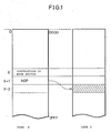
- each of banks A and B has addresses 0000H to FFFFH, and a memory area having addresses 0000H to 1FFFH is assigned for programs.
- this data processing system is a system of a pre-fetch scheme of fetching the next instruction during the execution of an instruction.
- the bank A is accessed by the CPU, so that steps (instructions) of the programs stored therein are sequentially read out and executed.
- a memory bank to be accessed is switched from the bank A to the bank B.
- This bank switching is performed by an additional bit to an address. More specifically, a combination of this additional bit and a counted value of an address counter (program counter) for addressing becomes a bank address. For example, an additional bit for the bank A is "0", and an additional bit for the bank B is "1".
- the bank A is accessed in the case of addresses 00000 to 0FFFF, while the bank B is accessed in the case of addresses 10000 to 1FFFF.
- a processing program similar to a subroutine includes an interrupt processing routine.
- This interrupt processing routine is similar to the subroutine in that it is an independent program stored in a memory area other than an area for the main routine, while being entirely different from the subroutine in that it is not related to the content of processing of the main routine.
- the subroutine and the interrupt processing routine are generically referred to as a subprogram in the sense that they are a separate program from the main routine.
- An interrupt control method in the memory bank switching scheme is disclosed in, for example, Japanese Patent Laying-Open Gazette No. 30050/1982.
- an interrupt processing program or a bank control program for interruption for designating a particular memory bank storing the interrupt processing program, a bank address or the like are stored in a common memory area provided separately from a plurality of memory banks. Interrupt processing is performed in accordance with a processing program stored in this common memory area and/or a particular memory bank.
- This prior art scheme cannot be applied to a system in which a region for storing a program associated with interrupt processing cannot be provided in a common memory area provided separately from memory banks, on a designing view of a system or depending on memory capacity of the system.
- the same interrupt processing program is forced to be stored in each of the memory banks. This causes the interrupt processing program to unnecessarily occupy a memory area extended by the memory bank switching scheme, so that a memory area for storing a desired processing program becomes narrow.
- the above described Japanese Patent Laying-Open Gazette No. 120543/1987 has proposed a method for designating a jump address using an instruction JMP (jump) in place of an instruction NOP subsequent to an instruction of bank switching to eliminate the necessity of address matching in the memory bank switching scheme.
- the jump address is designated only using the instruction JMP after bank switching step, and designation of a return address or the like is not considered at all.
- this method makes it difficult to perform a reliable operation.
- this prior art method cannot be applied to a subroutine executing method and an interrupt processing method in a system of a memory bank switching scheme.
- An object of the present invention is to provide a data processing apparatus of a memory bank switching scheme in which a program including switching of memory banks can be stored without consideration of address matching of the memory banks.
- Another object of the present invention is to provide a data processing apparatus of a bank switching scheme in which a program including switching steps of memory banks can be efficiently stored in a restricted memory area.
- Still another object of the present invention is to provide a data processing apparatus of a bank switching scheme in which a subroutine and an interrupt handling subroutine requiring switching of memory banks can be arranged in an arbitrary memory bank.
- Still another object of the present invention is to provide a subroutine executing apparatus of a bank switching scheme in which a subroutine in an arbitrary memory bank can be called from an arbitrary memory bank and the return to the original memory bank can be made.
- Still another object of the preset invention is to provide an interrupt processing executing apparatus of a bank switching scheme in which a program area can be efficiently utilized.
- Still another object of the present invention is to provide a subprogram executing method in a data processing apparatus of a bank switching scheme by which a subprogram can be called and the return can be made between arbitrary memory banks.
- Still another object of the present invention is to provide a method for executing a subroutine and an interrupt processing program in a data processing apparatus of a memory bank switching scheme by which a memory area can be efficiently utilized.
- Still another object of the present invention is to provide a subroutine executing method by which the execution time of a program requiring a subroutine requiring switching of memory banks can be shortened.
- a further object of the present invention is to provide a subprogram executing method including bank switching by which the same bank switching control program can be used commonly to a plurality of subprograms.
- a still further object of the present invention is to provide a subprogram executing method including bank switching by which memory banks can be switched in a few processing steps.
- the data processing apparatus of a bank switching scheme has a plurality of memory banks, a bank switching control program being stored in a memory area with the same addresses in each of the plurality of memory banks.
- the subprogram executing method comprises the steps of switching memory banks and reading out a bank switching control program in a second memory bank in accordance with a bank switching control program in a first memory bank when the execution of a subprogram in the second memory bank is required during the execution of a processing program in the first memory bank, calling a required subprogram in accordance with the read-out bank switching control program in the second memory bank, returning to the bank switching control program in the second memory bank after the execution of this required subprogram is completed, switching the memory banks from the second memory bank to the first memory bank and reading out the bank switching control program in the first memory bank in accordance with the returned bank switching control program in the second memory bank, and returning to the original processing program in accordance with the read-out bank switching control program in the first memory bank.
- a bank switching control program is stored only in the same address space in each of the memory banks, and switching of the memory banks, calling of the subprogram and the return to the original processing program are achieved in accordance with this bank switching control program.
- address matching of the main program and the subprogram need not be considered, so that the subprogram can be arranged in arbitrary address positions of the memory bank.
- the memory area can be efficiently utilized and the program development time can be shortened.
- the memory area can be utilized more efficiently.
- the memory banks can be switched in a few processing steps, i.e., at high speed.
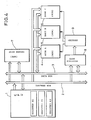
- Fig. 2 shows a schematic configuration of a main portion of a data processing system of a memory bank switching scheme according to a first embodiment of the present invention.
- a data processing system comprises a CPU 1 for performing data processing, a control operation or the like in accordance with an applied program, memory banks A4 and B5 for respectively storing a predetermined processing program, and a main memory 7 for storing various data, a user program loaded from an external apparatus (not shown), or the like.
- the memory bank A4 comprises a read only memory (ROM), which fixedly stores a predetermined first processing program inherent in the system.
- the memory bank B5 comprises a ROM, which fixedly stores a second processing program inherent to the system.
- the main memory 7 comprises a random access memory (RAM) such that the content thereof can be updated.
- RAM random access memory
- a bank register 8 for storing bank designation data for specifying a bank to be accessed, and a decoder 9 for selecting any one of the memory banks A4 and B5 depending on the content of the bank register 8 to bring the selected bank to an enable state.
- the decoder 9 has a general configuration, i.e., comprises a decoder of a NOR type or a NAND type. Although in the above described system configuration the memory banks A and B respectively comprise ROMs 4 and 5, the memory banks A and B may be provided on a single ROM chip.
- Each of the memory banks A4 and B5 comprises an area 90 for storing a bank switching control program (referred to as a bank switching manager hereinafter), and an area 100 for storing a predetermined processing program.
- the same address area (addresses 0 to 5 in Fig. 3) in each of the memory banks A4 and B5 is assigned to the area 90.
- the processing program storing areas 100 in the memory banks A4 and B5 store different processing programs.
- Figs. 2 and 3 description is made on an operation in which a subroutine in the memory bank B5 is called from a main routine in the memory bank A4 and executed.
- the operation flow is represented by arrows.
- a plurality of subroutines SUB 1, SUB 2, ... are stored in address positions independent of an address at which a subroutine call instruction CALL of the main routine in the memory bank A4 is stored.
- an instruction MOV BX, Y for transferring the content of a start address Y of a subroutine SUB 1 to the register BX (provided in the CPU 1 or the RAM 7, in Fig. 2 it is included in the CPU 1) is stored at an address X, and an instruction CALL 0 for calling a bank switching manager starting at the address 0 is stored at the next address X+1.
- an instruction for switching the memory banks from the bank A to the bank B is stored at the address 0
- an instruction JMP $ for jumping to the next address by eternal looping is stored at the address 1
- an instruction NOP is stored at the respective addresses 2 to 4
- an instruction RET for returning to the main routine after the completion of the subroutine is stored at the address 5.
- an instruction NOP is stored at the respective addresses 0, 1 and 5
- an instruction CALL BX for calling the content of the register BX is stored at the address 2
- an instruction of bank switching for switching the memory banks from the bank A to the bank B is stored at the address 3
- an instruction JMP $ is stored at the address 4.
- a subroutine starting at an address set in the register BX is called by the instruction CALL BX at the address 2.
- an instruction to be next executed after switching of the memory banks is the content of the address 1 in the memory bank A4.
- the CPU 1 sets bank designation data of the memory bank B5 by the bank switching instruction and writes the same in the bank register 7, and the decoder 8 decodes the data set in this bank register 7 to disable the memory bank A4 and enable the memory bank B5, so that bank switching is achieved.
- this substantial bank switching is completed during the execution of the instruction JMP $ at the address 1 in the memory bank A4.
- the instruction CALL BX at the address 2 in the memory bank B4 is executed after the instruction JMP $.
- the address Y which has been already stored in the register BX is read out by this CALL instruction, so that the subroutine SUB 1 starting at this address Y is executed.
- the bank switching instruction at the address (address 3) subsequent to the CALL instruction in the memory bank B5 is executed, so that bank switching is performed from the memory bank B5 to the memory bank A4 under the control of the CPU 1.
- the instruction RET at the address 5 in the memory bank A4 is then executed by the instruction JMP $ at the address 4 in the memory bank B5.
- the content of the next address (address X+2) subsequent to the CALL instruction in the memory bank A4 is read out and executed. Consequently, the return to the main routine in the memory bank A4 is completed, so that the program of this main routine are sequentially executed.
- an area for a bank switching manager is extended by two times of that shown in Fig. 3, to store the same switching manager as the bank switching manager (addresses 0 to 5) of the memory bank A4 in this extended area of the memory bank B5 and store the same switching manager as the bank switching manager shown in Fig. 3 of the memory bank B5 in the extended area of the memory bank A4.
- an instruction MOV for calling a subroutine and an instruction CALL for calling the bank switching manager stored in the extended area are stored in the main routine in the memory bank B5, as in the main routine in the memory bank A4.
- Fig. 4 shows, as an example, a schematic configuration with a system of a bank switching scheme comprising three memory banks.
- a memory bank C6 constituting a third memory bank, in addition to the configuration shown in Fig. 2.
- the memory bank C6 comprises a ROM.
- the memory banks A4, B5 and C6 store different processing programs.
- a resistor AH for storing return bank designation data
- a resistor AL for storing data for designating a memory bank which is the destination to be switched
- a register BX for storing a start address of a subroutine.
- the registers AH, AL and BX are provided in the CPU 1 as shown, or provided in a predetermined region in the main memory (RAM) 7.
- resistors A, B, C, D and the like for temporarily storing data to be processed are provided in the CPU 1.
- the registers A to D are suitably used as the registers AL, AH and BX.
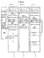
- Figs. 5 shows an example of the contents respectively stored in memory banks.
- Each of the memory banks A4, B5 and C6 comprises a bank switching manager storing area 90 and a processing program area 100 for storing a predetermined program.
- the same particular area in each of the memory banks A4, B5 and C6, i.e., an area at addresses 0 to (S-1) is assigned to the bank switching manager storing area 90.
- An area in the remaining addresses in each of the memory banks A4, B5 and C6 is assigned to the processing program area 100.
- the memory banks A4, B5 and C6 respectively store different processing programs.
- a bank switching manager roughly comprises first to fourth programs, which are respectively stored at addresses 0 to (P-1), addresses P to (Q-1), addresses Q to (R-1), and addresses R to (S-1).
- the first program stored at the addresses 0 to (P-1) comprises an instruction for saving its own bank designation data in a predetermined register which is, for example, the register AH as return bank designation data, and an instruction for decoding jump designation data saved in the predetermined register such as the register AL and jumping to a corresponding address in the second program (as described below).
- the second program stored in the addresses P to (Q-1) in each of the memory banks A4, B5 and C6 is used for actually switching to a jump bank.
- the second program comprises a combination of an NOP instruction and a JMP Q instruction and two bank switching instructions for switching the banks from its own bank to either one of the remaining two memory banks.
- an instruction for switching to the bank A, an instruction for switching to the bank B and an instruction for switching to the bank C are respectively stored at the same addresses in the memory banks A, B and C.
- the NOP instruction is stored at the same addresses in the banks which are the destinations to be switched by the bank switching instructions.
- the third programs at the addresses Q to (R-1) in the three memory banks are the same, each comprising an instruction for calling a subroutine starting at a jump address saved in the register BX and an instruction for decoding return bank designation data saved in the register AH to jump to a corresponding address in the fourth program (as described below).
- the fourth program at the addresses R to (S-1) is a return program for actual switching to a return bank.
- the fourth program has almost the same scheme as that of the second program, but differs from the second program in that an RET instruction is stored in place of the JMP instruction.
- An MOV instruction for saving jump bank designation data (specifying the bank C6) indicating a memory bank storing the subroutine SUB 1 is stored in an address X in the memory bank A4.
- An MOV instruction for saving a start address of the subroutine SUB 1 in the register BX as a jump address is stored at an address X+1.
- a CALL instruction for calling a bank switching manager (a first program) starting at the address 0 is stored at an address X+2. It should be noted that the address X for calling a subroutine in the main routine and the start address of the subroutine SUB 1 are entirely independent of each other. Description is now made on the operation. Arrows in Fig. 5 represent the operation flow.
- jump bank (memory bank C6) designation data is stored in the register AL by the MOV instruction at the address X.
- the start address Y of the subroutine SUB 1 is saved in the register BX.
- the content of the address 0 in the memory bank A4 is called, so that the bank switching manager in the memory bank A4 is executed.
- this bank switching manager its own memory bank number A is saved in the register AH as return bank designation data.
- a jumping bank number (in this case, the bank C) which has been already saved in the register AL is decoded, and then a jump takes place to a corresponding address in the second program in the memory bank A4. Since a jumping bank is the bank C6, a jump takes place to an address for executing the switching to the bank C in the second program, so that bank switching to the memory bank C6 is performed.
- a JMP Q instruction is stored subsequent to the NOP instruction.
- an address pointer (not shown) for outputting an address to be executed is not changed in its content at all at the time of bank switching.
- an instruction to be executed after completion of bank switching is the JMP Q instruction in the memory bank C6. Consequently, the content of the start address Y of the subroutine SUB1 saved in the register BX is read out in accordance with the instruction CALL BX at the address Q, so that the subroutine SUB 1 is executed.
- a return bank determining operation of the third program in the memory bank C6 is performed by an RET instruction at an address Y′ after the execution of the subroutine SUB 1 is completed.
- return bank determining operation return bank designation data saved in the register AH is first decoded, and a jump to a corresponding address of the fourth program in the memory bank C6 takes place in accordance with the result of the decoding.
- the return bank is the memory bank A4
- a jump to an instruction for switching to the bank A in the fourth program in the memory bank C6 takes place, so that switching is performed from the bank C6 to the bank A4.
- the return to the main routine in the memory bank A4 is made by the RET instruction of the fourth program in the memory bank A4.
- the content of the bank register 8 is changed by the bank switching instruction under the control of the CPU 1 and the decoder 9 enables a corresponding memory bank in accordance with this changed content of the bank register 8, so that bank switching is achieved.
- a subroutine in an arbitrary memory banks can be called from a main routine in any memory bank and executed.
- troublesome address matching of the main routine and the subroutine is not required.
- the subroutine can be arranged at an arbitrary address, so that working efficiency in developing a program can be significantly improved.
- bank switching can be accomplished in accordance with only a program stored in a particular address area, a program area for bank switching can be reduced.
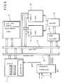
- Fig. 6 shows a main portion of a configuration associated with interrupt processing in a system with a memory bank switching scheme having two memory banks provided therein.
- an interrupt controller 20 is provided, in addition to the configuration shown in Fig. 2.
- the interrupt controller 20 monitors various interrupt signals, generates a signal INT for indicating occurrence of an interruption to apply the same to the CPU 1 at the time of occurrence of an interruption, and sends out to an address bus 2 a vector address corresponding to the type of the occurring interruption.
- An interrupt vector table storing a start address of each interrupt handler to be executed developed in a table form with respect to each vector address is stored in a predetermined area in the main memory 7.
- the CPU 1 interrupts a processing program in execution and reads out a start address corresponding to the vector address from this table, to execute a subprogram starting at the address read out from this table.
- Fig. 7 shows an example of a program stored in memory banks A and B.
- Fig. 7 shows only a program concerning a particular interruption out of a plurality of interruptions.
- an address X is designated to be executed in accordance with an interrupt vector table on the main memory 7 at the time of occurrence of this interruption.
- Each of the memory banks A4 and B5 comprises an area 90 for storing a bank switching control program (bank switching manager) and an area 100 for storing a predetermined processing program.
- the same address area (addresses 0 to 5 in Fig. 7) in each of the memory banks A4 and B5 is assigned to the bank switching manager storing area 90.
- the processing program area 100 in the memory bank A4 comprises an area (an area of addresses X to W) for storing an interrupt processing program 12 concerning a particular interruption and an area for storing a predetermined processing program. More specifically, an interrupt handling subroutine indicating the actual content of interrupt processing is stored in the area of the addresses Y to W in the memory bank A4, and a CALL instruction for calling this interrupt handling subroutine and an IRET instruction indicating the return from a subroutine to a main routine are respectively stored in the addresses X and X+1. A start address of the interrupt handling subroutine is the address Y. In addition, an RET instruction indicating the termination of a subroutine and the return to the main routine is stored at the address W.
- an interrupt control program 13 is stored at addresses X to Z.
- This interrupt control program 13 comprises a PUSH instruction for storing the content of the resistor BX in a stack (provided in the CPU 1), an MOV instruction for transferring to the register BX the start address Y of the interrupt handling routine, a CALL instruction for calling the bank switching manager starting at the address 0, a POP instruction for loading in the register BX the content stored in the stack, and an IRET instruction for returning from the interrupt handling subroutine to the main routine.
- an instruction for switching the banks from the bank B to the banks A a JMP $ instruction, an NOP instruction, and an RET instruction are respectively stored at the address 0, the address 1, the addresses 2 to 4, the address 5.
- a signal INT for indicating occurrence of an instruction is applied to the CPU 1 from the interrupt controller 20, and a vector address is sent out onto the address bus 2.
- the address X stored in the interrupt vector table in the main memory 7 is read out in accordance with this vector address, the content of the register BX is pushed into the stack, and an interrupt control program starting at the address X is executed by the CPU 1. More specifically, the start address Y of the interrupt subroutine is then transferred from the table to the register BX. Thereafter, the address 0 in the memory bank B5 is called so that the instruction at the address 0 is executed and then, the JMP $ instruction is executed.
- the memory banks are switched from the bank B5 to the bank A4, and the CALL instruction at the address 2 in the memory bank A4 is executed.
- the address Y stored in the register BX is accessed by this CALL instruction, so that an interrupt handling subroutine starting at the address Y is executed.
- the return to an address subsequent to the address of the CALL instruction of the bank switching manager in the memory bank A4 is made by the RET instruction at the address W.
- the content of the address 3 which is the destination of the return is a bank switching instruction.
- the memory banks are switched from the bank A4 to the bank B5 by the bank switching instruction together with the JMP $ instruction at the address 4 and then, the RET instruction at the address 5 in the bank B5 is executed.
- a POP instruction stored at an address subsequent to the address of the CALL instruction in the program 13 in the memory bank B5 is executed by this RET instruction. Consequently, the content set in the stack is loaded in the register BX.
- the IRET instruction is executed after this loading, and the execution of an interrupted main routine in the memory bank B4 is resumed.
- an MOV instruction for transferring to the register BX a start address of an interrupt processing program to be executed is stored at a particular address (i.e., an address in a table corresponding to a vector address) designated by the interruption, processing of the interruption can be performed using the bank switching manager in the area 90.
- the transition to the address 0 may be made using the JMP instruction in place of the CALL instruction.
- the POP instruction and the IRET instruction are executed in the bank switching manager of the memory bank A4 and the return to the interrupted processing program in the memory bank B5 is made without through the interrupt control program 13 after bank switching is performed by the bank switching manager in the memory bank B5 so that the interrupt handling subroutine is executed.
- the POP BX instruction, the bank switching instruction and the IRET instruction are stored at the addresses 3 to 5 in the area 90 in the bank A4.
- FIG. 8 differs greatly from the method shown in Fig. 7 in two respects.
- the first respect is that an interrupt control program (13 in Fig. 7) for transferring to a predetermined register a start address of an interrupt handling subroutine to be executed is not stored in the method shown in Fig. 8. More specifically, in the method shown in Fig. 8, a bank switching manager in the memory bank B5 is immediately executed by a JMP instruction at an address X.
- the second respect is to directly designate the address in calling the interrupt handling subroutine in the bank switching manager of the memory bank A4 in the method shown in Fig. 8. More specifically, the method shown in Fig. 8 differs from the method shown in Fig. 7 in that a predetermined register BX is not used and a CALL Y instruction is used in place of the CALL BX instruction.
- the schemes (or program structure) shown in Figs. 7 and 8 are substantially the same except for the foregoing.
- Figs. 7 and 8 can be naturally used in combination depending on the type of an interruption.
- the return to an interrupted processing program is made by an IRET instruction in a bank switching manager the memory bank B5
- a scheme may be used in which a CALL O instruction is stored at an address X in the memory bank B4, as shown in a parentheses in Fig. 8, in place of the JMP O instruction, and the return to an interrupted processing program is further made using an RET instruction in place of the IRET instruction in the bank switching manager.
- Fig. 9 shows a schematic configuration of the system.
- a memory bank C6 comprising a ROM, in addition to the configuration shown in Fig. 6.
- the bank register 8 stores bank designation data for designating any one of memory banks A4, B5 and C6.
- the decoder 9 decodes the bank designation data in the bank resistor 8, to enable only the corresponding designated memory bank.
- the other configuration is substantially the same as that shown in Fig. 6.
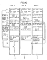
- Fig. 10 is a diagram showing an example of the contents respectively stored in the memory banks A4, B5 and C6.
- Fig. 10 shows a scheme in which particular interrupt processing out of a plurality of interrupt processing is performed.
- a start address X of a subroutine for this particular interrupt processing is designated by an interrupt vector table developed in a predetermined region on the main memory 7. Since the main memory 7 is an RAM, this interrupt vector table is stored in a predetermined region of the main memory 7 in accordance with a bootstrap program when the system is powered on.
- each of the memory banks A4, B5 and C6 comprises a bank switching manager storing area 90 and a processing program area 100 for storing a predetermined processing program.
- the same address area in each of the memory banks A4, B5 and C6, i.e., an area at addresses 0 to (S-1) is assigned to the area 90.
- a bank switching manager has the same scheme as that for executing the subroutine shown in Fig. 5. More specifically, the bank switching manager, the details of which are not repeated, comprises a first program stored in addresses 0 to (P-1) for setting a return bank and a jumping bank, a second program stored in addresses P to (Q-1) for actual bank switching to the jumping bank, a third program stored in addresses Q to (R-1) for setting a start address of an interrupt handling subroutine and determining the return bank, and a fourth program stored in addresses R to (S-1) for actual bank switching to the return bank.
- An interrupt processing program 33 concerning a particular interruption is stored in an area at addresses X to W in the memory bank C.
- the interrupt processing program 33 has a CALL Y instruction stored at an address X, an IRET instruction stored at an address X+1, and an interrupt handling subroutine stored in addresses Y to W and indicating the content of actual interrupt processing. Description is now made on a processing operation to occur when an interruption occurs during the execution of a processing program in either one of the main banks A4 and B5. In Fig. 10, an example of the operation flow is represented by arrows.
- the address X is read out from the table in the main memory 7 in response to a vector address from the interrupt controller 20, so that the content of this address X is executed by the CPU 1.
- An area at addresses X to Z in each of the memory banks A4 and B5 stores an interrupt control program comprising an MOV instruction for saving in the register AL bank designating data BANK No. A having a corresponding interrupt processing program, an MOV instruction for saving in the register BX the first address Y of the interrupt handling subroutine, a CALL instruction for calling a bank switching manager, and an IRET instruction indicating the return to the interrupted address.
- a JMP Q instruction is stored following to an NOP instruction.
- an interrupt handling subroutine starting at the address Y stored in the register BX is called and executed.
- a return address saved in the register AH is decoded in accordance with the RET instruction at the address W.
- a return bank is the memory bank A4
- a jump to an address for returning to the memory bank A takes place, so that bank switching to the memory bank A4 is performed.
- the return to the interrupt control program (IRET instruction) in the memory bank A is made by an RET instruction in the memory bank A4, so that the return to a processing program which is executed before the interruption is made through this control program.
- bank switching can be performed from an arbitrary bank to an other arbitrary bank in accordance with bank switching managers stored in the same address area of the banks.
- an interrupt control program for saving jumping bank designation data and/or a jumping address for an interrupt handling program to be executed in the register AL and/or the register BX is stored at a particular address designated by the interruption, interrupt control can be performed utilizing in common the bank switching manager stored in the area 90.
- Fig. 11 shows a scheme in which the scheme shown in Fig. 8 is applied to a system having three memory banks.
- a bank switching manager is provided for a particular interruption only, as in the scheme shown in Fig. 8. More specifically, jump bank designation data and a jumping address (a first address of an interrupt handling subroutine) for bank switching are respectively fixedly stored in a memory bank C6 and an address Y in a bank switching manager of each of the memory banks.
- jump bank designation data and a jumping address (a first address of an interrupt handling subroutine) for bank switching are respectively fixedly stored in a memory bank C6 and an address Y in a bank switching manager of each of the memory banks.
- the first address of the interrupt handling subroutine is stored in a register BX before the transition to the bank switching manager after generation of an interruption, and the content of the register BX is called to execute the interrupt handling subroutine after bank switching by the bank switching manager.
- interrupt processing can be performed without increasing the number of bank switching managers.
- a plurality of control programs begining at the address X in each of the memory banks A4 and B5 are provided corresponding to the plurality of interrupt processings.
- the number of the above described bank destination data is only increased.
- the system can be easily extended to a system having four or more memory banks therein.
- a bank switching manager is stored in the same address area in each of memory banks and bank switching is performed in accordance with this bank switching manager, so that required interrupt processing can be performed.
- interrupt processing can be performed utilizing an interrupt handling program stored in a particular memory bank and an interrupted processing program can be resumed. Consequently, a large memory area can be used as a program area for storing a main processing program, so that the memory area can be efficiently utilized.
- long processing programs and desired and required processing programs are all stored in the memory bank.
Landscapes
- Engineering & Computer Science (AREA)
- Software Systems (AREA)
- Theoretical Computer Science (AREA)
- Physics & Mathematics (AREA)
- General Engineering & Computer Science (AREA)
- General Physics & Mathematics (AREA)
- Executing Machine-Instructions (AREA)
Applications Claiming Priority (8)
| Application Number | Priority Date | Filing Date | Title |
|---|---|---|---|
| JP63041535A JPH01216428A (ja) | 1988-02-24 | 1988-02-24 | メモリバンクのサブルーチン実行方式 |
| JP41535/88 | 1988-02-24 | ||
| JP41536/88 | 1988-02-24 | ||
| JP63041536A JPH01216433A (ja) | 1988-02-24 | 1988-02-24 | 割込制御方式 |
| JP122313/88 | 1988-05-19 | ||
| JP63122313A JPH01292432A (ja) | 1988-05-19 | 1988-05-19 | メモリバンクのサブルーチン実行方式 |
| JP129052/88 | 1988-05-26 | ||
| JP63129052A JPH01297732A (ja) | 1988-05-26 | 1988-05-26 | 割込制御方式 |
Publications (3)
| Publication Number | Publication Date |
|---|---|
| EP0330226A2 true EP0330226A2 (de) | 1989-08-30 |
| EP0330226A3 EP0330226A3 (de) | 1991-10-09 |
| EP0330226B1 EP0330226B1 (de) | 1995-11-08 |
Family
ID=27461073
Family Applications (1)
| Application Number | Title | Priority Date | Filing Date |
|---|---|---|---|
| EP89103296A Expired - Lifetime EP0330226B1 (de) | 1988-02-24 | 1989-02-24 | Vorrichtung und Verfahren zur Ausführung eines Unterprogramms in einem Datenverarbeitungssystem mit Blockumschaltung |
Country Status (4)
| Country | Link |
|---|---|
| US (1) | US5146581A (de) |
| EP (1) | EP0330226B1 (de) |
| KR (1) | KR920006614B1 (de) |
| DE (1) | DE68924719T2 (de) |
Cited By (5)
| Publication number | Priority date | Publication date | Assignee | Title |
|---|---|---|---|---|
| EP0576027A3 (de) * | 1992-06-26 | 1995-02-01 | Tokyo Shibaura Electric Co | Tragbaren Computer mit ikonenbasierter Menuselektion. |
| WO1995021413A1 (de) * | 1994-02-03 | 1995-08-10 | Siemens Aktiengesellschaft | Datenverarbeitungsanlage mit einem von einem controller adressierbaren arbeitsspeicher |
| GB2289148A (en) * | 1994-04-29 | 1995-11-08 | Motorola As | Microprocessor and banked memory. |
| FR2820223A1 (fr) * | 2001-01-31 | 2002-08-02 | St Microelectronics Sa | Microprocesseur comprenant des moyens de gestion et d'acces a un espace adressable pagine |
| EP1251431A3 (de) * | 2001-04-18 | 2004-04-14 | NEC Electronics Corporation | Verminderung von Bankumschaltungs-Instruktionen in einem Hauptspeicher eines Datenverarbeitungsystems mit Hauptspeicher und mehreren Speicherbänken |
Families Citing this family (16)
| Publication number | Priority date | Publication date | Assignee | Title |
|---|---|---|---|---|
| CA2003821C (en) * | 1989-04-20 | 1996-12-03 | Richard J. Molnar | Process controller single memory chip shadowing technique |
| US5253354A (en) * | 1990-08-31 | 1993-10-12 | Advanced Micro Devices, Inc. | Row address generator for defective DRAMS including an upper and lower memory device |
| US5293591A (en) * | 1991-06-10 | 1994-03-08 | Advanced Micro Devices, Inc. | Processing system including memory selection of multiple memories and method in an interrupt environment |
| JP3092116B2 (ja) * | 1991-08-26 | 2000-09-25 | 日本電気株式会社 | プログラム変更方式 |
| TW241346B (de) * | 1991-10-15 | 1995-02-21 | Bull Hn Information Syst | |
| US5557766A (en) * | 1991-10-21 | 1996-09-17 | Kabushiki Kaisha Toshiba | High-speed processor for handling multiple interrupts utilizing an exclusive-use bus and current and previous bank pointers to specify a return bank |
| DE69231176T2 (de) * | 1991-12-23 | 2000-11-23 | Microsoft Corp., Redmond | Verfahren zum Integrieren eines diskreten Unterprogramms in ein Hauptprogramm |
| CA2080159C (en) * | 1992-10-08 | 1998-09-15 | Paul Alan Gresham | Digital signal processor interface |
| US5802544A (en) * | 1995-06-07 | 1998-09-01 | International Business Machines Corporation | Addressing multiple removable memory modules by remapping slot addresses |
| JP2000195262A (ja) * | 1998-12-25 | 2000-07-14 | Internatl Business Mach Corp <Ibm> | Sdram及びsdramのデ―タ・アクセス方法 |
| TWI284806B (en) * | 2003-02-27 | 2007-08-01 | Mediatek Inc | Method for managing external memory of a processor and chip for managing external memory |
| TWI222597B (en) * | 2003-03-14 | 2004-10-21 | Mediatek Inc | Method for accessing external memory of a microprocessor |
| JP5319238B2 (ja) * | 2008-10-29 | 2013-10-16 | 真二 栗本 | 情報処理システム、情報処理装置、情報処理方法、および情報処理プログラム |
| DE102018128045A1 (de) * | 2018-11-09 | 2020-05-14 | Infineon Technologies Ag | Behandlung von Ausnahmen in einem Programm |
| US20200364052A1 (en) * | 2019-05-15 | 2020-11-19 | Western Digital Technologies, Inc. | Branch penalty reduction using memory circuit |
| US11550577B2 (en) * | 2019-05-15 | 2023-01-10 | Western Digital Technologies, Inc. | Memory circuit for halting a program counter while fetching an instruction sequence from memory |
Family Cites Families (16)
| Publication number | Priority date | Publication date | Assignee | Title |
|---|---|---|---|---|
| US3866182A (en) * | 1968-10-17 | 1975-02-11 | Fujitsu Ltd | System for transferring information between memory banks |
| US3737860A (en) * | 1972-04-13 | 1973-06-05 | Honeywell Inf Systems | Memory bank addressing |
| US4340932A (en) * | 1978-05-17 | 1982-07-20 | Harris Corporation | Dual mapping memory expansion unit |
| US4368515A (en) * | 1981-05-07 | 1983-01-11 | Atari, Inc. | Bank switchable memory system |
| US4503491A (en) * | 1981-06-29 | 1985-03-05 | Matsushita Electric Industrial Co., Ltd. | Computer with expanded addressing capability |
| US4481570A (en) * | 1981-08-07 | 1984-11-06 | The United States Of America As Represented By The Administrator Of The National Aeronautics And Space Administration | Automatic multi-banking of memory for microprocessors |
| JPS60157646A (ja) * | 1984-01-27 | 1985-08-17 | Mitsubishi Electric Corp | メモリバンク切換装置 |
| US4725945A (en) * | 1984-09-18 | 1988-02-16 | International Business Machines Corp. | Distributed cache in dynamic rams |
| US4744048A (en) * | 1985-10-09 | 1988-05-10 | American Telephone And Telegraph Company | Display context switching arrangement |
| JPS6289149A (ja) * | 1985-10-15 | 1987-04-23 | Agency Of Ind Science & Technol | 多ポ−トメモリシステム |
| FR2591775B1 (fr) * | 1985-12-12 | 1988-03-04 | Inst Nat Rech Inf Automat | Dispositif electronique formant memoire stable rapide perfectionnee |
| US4755935A (en) * | 1986-01-27 | 1988-07-05 | Schlumberger Technology Corporation | Prefetch memory system having next-instruction buffer which stores target tracks of jumps prior to CPU access of instruction |
| JPS6356754A (ja) * | 1986-08-28 | 1988-03-11 | Toshiba Corp | 入出力チヤネル |
| CA1330596C (en) * | 1986-11-19 | 1994-07-05 | Yoshiaki Nakanishi | Memory cartridge and data processing apparatus |
| US4933846A (en) * | 1987-04-24 | 1990-06-12 | Network Systems Corporation | Network communications adapter with dual interleaved memory banks servicing multiple processors |
| DE68925376T2 (de) * | 1988-04-20 | 1996-09-05 | Sanyo Electric Co | In Direktabbildung und in Bankabbildung wirksamer Informationsprozessor und Verfahren zum Schalten der Abbildungsschemas |
-
1989
- 1989-02-22 US US07/313,677 patent/US5146581A/en not_active Expired - Fee Related
- 1989-02-24 KR KR1019890002294A patent/KR920006614B1/ko not_active Expired
- 1989-02-24 EP EP89103296A patent/EP0330226B1/de not_active Expired - Lifetime
- 1989-02-24 DE DE68924719T patent/DE68924719T2/de not_active Expired - Fee Related
Cited By (8)
| Publication number | Priority date | Publication date | Assignee | Title |
|---|---|---|---|---|
| EP0576027A3 (de) * | 1992-06-26 | 1995-02-01 | Tokyo Shibaura Electric Co | Tragbaren Computer mit ikonenbasierter Menuselektion. |
| US5537531A (en) * | 1992-06-26 | 1996-07-16 | Kabushiki Kaisha Toshiba | Portable computer with a bank switch for switching between a ROM and a memory, both allocated to the same address space, by changing a port address of a keyboard controller |
| WO1995021413A1 (de) * | 1994-02-03 | 1995-08-10 | Siemens Aktiengesellschaft | Datenverarbeitungsanlage mit einem von einem controller adressierbaren arbeitsspeicher |
| GB2289148A (en) * | 1994-04-29 | 1995-11-08 | Motorola As | Microprocessor and banked memory. |
| GB2289148B (en) * | 1994-04-29 | 1998-08-05 | Motorola As | Electronic device with microprocessor and banked memory and method of operation |
| FR2820223A1 (fr) * | 2001-01-31 | 2002-08-02 | St Microelectronics Sa | Microprocesseur comprenant des moyens de gestion et d'acces a un espace adressable pagine |
| EP1251431A3 (de) * | 2001-04-18 | 2004-04-14 | NEC Electronics Corporation | Verminderung von Bankumschaltungs-Instruktionen in einem Hauptspeicher eines Datenverarbeitungsystems mit Hauptspeicher und mehreren Speicherbänken |
| US6772271B2 (en) | 2001-04-18 | 2004-08-03 | Nec Electronics Corporation | Reduction of bank switching instructions in main memory of data processing apparatus having main memory and plural memory |
Also Published As
| Publication number | Publication date |
|---|---|
| EP0330226A3 (de) | 1991-10-09 |
| KR920006614B1 (ko) | 1992-08-10 |
| KR890013557A (ko) | 1989-09-23 |
| DE68924719T2 (de) | 1996-05-23 |
| DE68924719D1 (de) | 1995-12-14 |
| US5146581A (en) | 1992-09-08 |
| EP0330226B1 (de) | 1995-11-08 |
Similar Documents
| Publication | Publication Date | Title |
|---|---|---|
| US5146581A (en) | Subprogram executing data processing system having bank switching control storing in the same address area in each of memory banks | |
| US5214786A (en) | RISC system performing calls and returns without saving or restoring window pointers and delaying saving until multi-register areas are filled | |
| JP3787167B2 (ja) | フラッシュメモリ | |
| US4755935A (en) | Prefetch memory system having next-instruction buffer which stores target tracks of jumps prior to CPU access of instruction | |
| EP0538817A2 (de) | Hochgeschwindigkeitsprozessor zum fähiger Abhandeln mehrerer Unterbrechungen | |
| EP0464615A2 (de) | Mikrorechner ausgestattet mit einer DMA-Steuerung | |
| US4274138A (en) | Stored program control system with switching between instruction word systems | |
| US5628026A (en) | Multi-dimensional data transfer in a data processing system and method therefor | |
| JPH02267634A (ja) | 割込み処理装置 | |
| KR100875377B1 (ko) | 처리 시스템에서 스택 팝 및 푸쉬 동작들을 수행하는 장치 및 방법 | |
| US6088787A (en) | Enhanced program counter stack for multi-tasking central processing unit | |
| KR19980069757A (ko) | 마이크로프로세서 및 멀티프로세서 시스템 | |
| EP2054800A2 (de) | Zugangsschaltung für flash-speicher | |
| JPH0332818B2 (de) | ||
| US5127096A (en) | Information processor operative both in direct mapping and in bank mapping, and the method of switching the mapping schemes | |
| US5274776A (en) | Information processing system having mode signal holding means and selecting operand access mode based on mode signal indicating type of currently executed instruction | |
| JP2001005676A (ja) | 割り込み処理装置 | |
| JPH0381179B2 (de) | ||
| US4816992A (en) | Method of operating a data processing system in response to an interrupt | |
| JP2001256044A (ja) | データ処理装置 | |
| WO2022034063A1 (en) | Processing apparatus | |
| US5675776A (en) | Data processor using FIFO memories for routing operations to parallel operational units | |
| US5557772A (en) | Data processing apparatus including a register storing a parameter and a microinstruction execution arrangement including a correction arrangement for causing a first value of the parameter to be change to a second, correct value | |
| EP0915416B1 (de) | Anordnung und Verfahren, die es ermöglichen, einen Zweiwortbefehl in einem einzelnen Zyklus durchzuführen | |
| JPH0342723A (ja) | データ処理装置 |
Legal Events
| Date | Code | Title | Description |
|---|---|---|---|
| PUAI | Public reference made under article 153(3) epc to a published international application that has entered the european phase |
Free format text: ORIGINAL CODE: 0009012 |
|
| AK | Designated contracting states |
Kind code of ref document: A2 Designated state(s): DE FR GB |
|
| 17P | Request for examination filed |
Effective date: 19901228 |
|
| PUAL | Search report despatched |
Free format text: ORIGINAL CODE: 0009013 |
|
| AK | Designated contracting states |
Kind code of ref document: A3 Designated state(s): DE FR GB |
|
| 17Q | First examination report despatched |
Effective date: 19930921 |
|
| GRAA | (expected) grant |
Free format text: ORIGINAL CODE: 0009210 |
|
| AK | Designated contracting states |
Kind code of ref document: B1 Designated state(s): DE FR GB |
|
| REF | Corresponds to: |
Ref document number: 68924719 Country of ref document: DE Date of ref document: 19951214 |
|
| ET | Fr: translation filed | ||
| PLBE | No opposition filed within time limit |
Free format text: ORIGINAL CODE: 0009261 |
|
| STAA | Information on the status of an ep patent application or granted ep patent |
Free format text: STATUS: NO OPPOSITION FILED WITHIN TIME LIMIT |
|
| 26N | No opposition filed | ||
| REG | Reference to a national code |
Ref country code: GB Ref legal event code: IF02 |
|
| PGFP | Annual fee paid to national office [announced via postgrant information from national office to epo] |
Ref country code: FR Payment date: 20030210 Year of fee payment: 15 |
|
| PGFP | Annual fee paid to national office [announced via postgrant information from national office to epo] |
Ref country code: GB Payment date: 20030219 Year of fee payment: 15 |
|
| PGFP | Annual fee paid to national office [announced via postgrant information from national office to epo] |
Ref country code: DE Payment date: 20030306 Year of fee payment: 15 |
|
| PG25 | Lapsed in a contracting state [announced via postgrant information from national office to epo] |
Ref country code: GB Free format text: LAPSE BECAUSE OF NON-PAYMENT OF DUE FEES Effective date: 20040224 |
|
| PG25 | Lapsed in a contracting state [announced via postgrant information from national office to epo] |
Ref country code: DE Free format text: LAPSE BECAUSE OF NON-PAYMENT OF DUE FEES Effective date: 20040901 |
|
| GBPC | Gb: european patent ceased through non-payment of renewal fee |
Effective date: 20040224 |
|
| PG25 | Lapsed in a contracting state [announced via postgrant information from national office to epo] |
Ref country code: FR Free format text: LAPSE BECAUSE OF NON-PAYMENT OF DUE FEES Effective date: 20041029 |
|
| REG | Reference to a national code |
Ref country code: FR Ref legal event code: ST |