EP0332103A2 - Appareil pour lire des documents en plusieurs couleurs pour fac-similé en plusieurs couleurs - Google Patents
Appareil pour lire des documents en plusieurs couleurs pour fac-similé en plusieurs couleurs Download PDFInfo
- Publication number
- EP0332103A2 EP0332103A2 EP89103885A EP89103885A EP0332103A2 EP 0332103 A2 EP0332103 A2 EP 0332103A2 EP 89103885 A EP89103885 A EP 89103885A EP 89103885 A EP89103885 A EP 89103885A EP 0332103 A2 EP0332103 A2 EP 0332103A2
- Authority
- EP
- European Patent Office
- Prior art keywords
- colour
- document
- line
- black
- reading apparatus
- Prior art date
- Legal status (The legal status is an assumption and is not a legal conclusion. Google has not performed a legal analysis and makes no representation as to the accuracy of the status listed.)
- Granted
Links
Images


Classifications
-
- H—ELECTRICITY
- H04—ELECTRIC COMMUNICATION TECHNIQUE
- H04N—PICTORIAL COMMUNICATION, e.g. TELEVISION
- H04N1/00—Scanning, transmission or reproduction of documents or the like, e.g. facsimile transmission; Details thereof
- H04N1/40—Picture signal circuits
- H04N1/40012—Conversion of colour to monochrome
-
- H—ELECTRICITY
- H04—ELECTRIC COMMUNICATION TECHNIQUE
- H04N—PICTORIAL COMMUNICATION, e.g. TELEVISION
- H04N1/00—Scanning, transmission or reproduction of documents or the like, e.g. facsimile transmission; Details thereof
- H04N1/46—Colour picture communication systems
- H04N1/48—Picture signal generators
- H04N1/482—Picture signal generators using the same detector device sequentially for different colour components
- H04N1/484—Picture signal generators using the same detector device sequentially for different colour components with sequential colour illumination of the original
-
- H—ELECTRICITY
- H04—ELECTRIC COMMUNICATION TECHNIQUE
- H04N—PICTORIAL COMMUNICATION, e.g. TELEVISION
- H04N1/00—Scanning, transmission or reproduction of documents or the like, e.g. facsimile transmission; Details thereof
- H04N1/46—Colour picture communication systems
- H04N1/56—Processing of colour picture signals
-
- H—ELECTRICITY
- H04—ELECTRIC COMMUNICATION TECHNIQUE
- H04N—PICTORIAL COMMUNICATION, e.g. TELEVISION
- H04N1/00—Scanning, transmission or reproduction of documents or the like, e.g. facsimile transmission; Details thereof
- H04N1/46—Colour picture communication systems
- H04N1/64—Systems for the transmission or the storage of the colour picture signal; Details therefor, e.g. coding or decoding means therefor
Definitions
- the present invention generally relates to a facsimile system for transmitting electrically document data and more particularly to a document reading apparatus, facsimile equipment and LSI circuits suited profitably for processing multi-colour document data.
- a system for reading colour pictures by using a plurality of light sources having different spectral characteristics has already been proposed, as disclosed in JP-A-59-189775. Besides, such a colour picture reading system is also proposed in which at least one of the light sources is continuously energized throughout a whole period during which reading operation is performed.
- the distortion correcting circuit of the prior art requires a relatively large number of peripheral circuitries because the distortion correcting LSI for the monochromatic facsimile is employed.
- a first object of the present invention is to provide a document reading apparatus for facsimile equipment in which erroneous colour identification or discrimination for colour separation due to variation in the quantity of light emitted by light sources in the course of time lapse and/or as a function of change in temperature can positively be excluded.
- a second object of the present invention is to provide a facsimile system in which in case multi-colour document data are to be transmitted to a conventional monochromatic facsimile apparatus, the different colour data are transmitted as the signals capable of representing the different colours in terms of correspondingly different monochromatic patterns.
- a third object of the present invention is to provide a distortion correcting LSI circuit for use in a multi-colour facsimile which circuit can be implemented in a simplified circuit configuration for correcting a shading distortion.
- a fourth object of the present invention is to provide a multi-colour facsimile system equipped with an apparatus capable of inputting a correction reference signal for the shading correction in the course of a document reading operation.
- the first object of the present invention mentioned above can be achieved by a multi-colour document reading apparatus including means for detecting variation or change in the quantity of light emitted by illuminating light sources having different spectral characteristics, wherein the variation in the light quantity is utilized as control parameters for the colour separation.
- the second mentioned object of the present invention can be achieved by providing a multi-colour facsimile system imparted with an operation mode for transmitting multi-colour document data by synthesising them to monochromatic patterns corresponding to respective colours upon transmission to a conventional monochromatic facsimile in addition to a mode of transmitting multi-colour document data in the form of separated colour signals.
- the distortion correcting LSI circuit is so implemented as to store a plurality of shading waveforms which are regenerated individually and separately through switching means.
- a data for reference colour is additionally provided on a distortion correcting sheet or plate at a location outside of a region where the document is to be read.
- the means for detecting the change in the quantity of illumination at the document reading part continues to detect the quantity of light throughout the document reading period. Accordingly, even when the quantity of light changes in the course of reading a sheet of document, the colour separation circuit can be protected against erroneous operation, whereby colour identification can be realized with high reliability and certainty.
- the distortion correcting LSI circuit can store reference shading waveforms for the shading correction of red and black data, respectively, the necessity for supplying a number of times the reference shading waveforms is eliminated, whereby the processing time can correspondingly be reduced, while the number of external circuits as required can be decreased.
- a predetermined region of a document 4 carrying colour information and disposed at a predetermined reading position is illuminated by means of two sources having different spectral characteristics such as, for example, a light emission diode (LED) array 2 and a fluorescent lamp 1, where by a light or optical image of the abovementioned predetermined region of the document 4 is focussed onto an image sensor 6 through a lens 5.
- the LED array 2 is turned on and off at a timing corresponding to a one-line reading period by an on/off switch circuit 7, as will hereinafter be described in more detail.
- a distortion correcting circuit 8 performs correction of distortion and digitization of the signal outputted from the image sensor 6, the output signal of the distortion correcting circuit 8 being then supplied to both a colour separating circuit 9 and a light quantity ratio detecting circuit 12.
- the ratio of the quantity of light between the fluorescent lamp 1 and the LED array 2 is arithmetically determined on the basis of the quantity of light available from illumination with only the fluorescent lamp 1 and the quantity of light available when both of the fluorescent lamp 1 and the LED array 2 are simultaneously turned on for the illumination.
- the result of the arithmetic operation executed by the light quantity ratio detecting circuit 12 is supplied to the colour separating circuit 9.
- colour signals corresponding to black and red are discriminatively detected on the basis of the data supplied from the distortion correcting circuit 8 and the result of the arithmetic operation performed by the light quantity ratio detecting part 12, whereupon both the colour signals are separated from each other.
- the signals resulting from the colour separation are coded by a transmitting unit 10 to be transmitted externally by way of a transmission path 13 such as a telephone line.
- a transmission path 13 such as a telephone line.
- the red colour signal and the black colour signal separated each other on the line-by-line basis are transmitted in series.
- the red and black colour signals may be transmitted in series in a packet for every predetermined number of lines on the document.
- the colour signal incoming from other facsimile equipment is decoded in the transmitting/receiving unit 10, the results of the decoding being recorded by a recorder 11.
- shading waveforms changing-over of shading waveforms is taught because there are employed such light sources (i.e. the fluorescent lamp and the LED array) which exhibit remarkable difference in the shading waveform.
- the term "shading" should be elucidated.
- low-frequency noise is contained in the picture or video signal resulting from the photo-electric conversion because of various causes such as nonuniformity in luminance of the illuminating light sources used for reading the document, lowering of peripheral luminous intensity brought about by the lens system and/or nonlinearity in the sensitivity of the image sensor.
- Such low-frequency noise is referred to as the shading or shading waveform.
- the shading not only assumes different waveforms in dependence on the types of the light sources but also vary even in one and the same light source as a function of time elapse immediately following the turn-on of the light source. Accordingly, a reference shading waveform used for eliminating error ascribable to the shading effect should preferably be corrected with an appropriate timing.
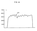
- An example of the shading waveform in a picture signal obtained by using a LED illumination is illustrated in Fig. 14.
- the shading waveform resulting from the illumination with a fluorescent lamp is of a smooth drum-like form.
- the synthesized shading waveform produced when both the fluorescent lamp and the LED are simultaneously lit assumes a waveform in which saw waves of small amplitudes and short period are superposed on the drum-like shading waveform produced upon illumination with the fluorescent lamp, as will be seen in Fig. 14.
- Fig. 2 illustrates in a flow chart a document read processing executed by the system shown in Fig. 1.
- the fluorescent lamp 1 is first lit (step 201).
- a document supporting plate coloured uniformly in white which also serves as a document feeding plate is read under illumination only by the fluorescent lamp 1, whereupon the signal waveform outputted from the image sensor 6 is stored as a reference shading waveform SHO for the data in black (step 202).
- the LED array 2 is lit (step 203), and the corresponding signal waveform produced by the image sensor 6 is stored as a reference shading waveform SHI for the data in red (step 204).
- the LED array 2 is then turned off (step 205).
- a document to be next transmitted is checked at a step 206.
- This can be accomplished by determining whether a signal DET-A produced by a switch 21 (Fig. 1) actuated in response to the presence of the succeeding document 20 is on (present) or not. When the signal DET-A is on, this means that the document to be transmitted is present. Accordingly, it is then checked whether or not the document 20 is in the reading position at which the document is to be read. This can be realized by determining whether or not a signal BET-B produced by a switch 22 (shown in Fig. 1) actuated in response to the presence of the document at the reading position is on (step 207).
- a motor PM (not shown) for document transportation is driven until the signal DET-B is detected (step 208), to thereby feed the document to the reading position.
- the processing proceeds to a step 209 where the reference shading waveform SHO for the data in black is regenerated to be referred to for correcting the shading distortion for-the data in black inputted by reading the document 20 under illumination by the fluorescent lamp 1 (step 210), the level of the data signal undergone the shading distortion correction being then determined.
- the LED 2 is lit (step 211), and the reference shading waveform SHI for the data in red is regenerated (step 212).
- the reference shading waveform SHI the shading distortion of the red data signal inputted subsequently is corrected, being followed by the determination of the level of the resulting red data signal (step 213).
- the LED array 2 is turned off (step 214).
- the motor is driven by one step to feed the document by a predetermined distance (step 215), whereupon it is checked with the aid of the signal DET-B whether the reading operation of the document has been completed (step 216).
- the processing returns to the step 206 where it is decided whether or not a document next to be transmitted is present or not. In case the next document is present, the step 207 is regained, whereupon the sequence or routine of the steps 209 to 216 is repeated. Otherwise, the fluorescent lamp 1 is turned off (step 217). The document reading operation thus comes to an end.
- Fig. 3 is a timing diagram for illustrating a sequence of the operations involved in the document reading operation described above.
- the document reading operation is started when the document read enabling signal DET-B is detected, as shown as (f) in Fig. 3.
- the fluorescent lamp is lit as shown at (e) and the reference shading waveform SHO to be referred to when the data in black is read is regenerated.
- a line synchronizing signal (a) is generated to read the data in black (b).
- the LED array is turned on, as shown at (d)
- the reference shading waveform SHI to be consulted upon reading the data in red is regenerated and the data in red is read as shown at (b).
- the LED is turned off upon completion of the document read operation for one line.
- the motor trigger signal (c) is again activated for feeding the document by the inter-line distance, whereupon the data reading operation is performed for the next line of the document by repeating the operation sequence mentioned above.
- the document read operation is repeated on a line-by-line base so long as the document is resident at the reading region.
- Figs. 4A and 4B illustrate the concept underlying the colour separation. More particularly, Fig. 4A shows signal waveforms produced upon reading data in red (R), green (G), blue (B) and black (BL), respectively, under illumination with a green fluorescent lamp.
- V W represents the white level corresponding to a wholly white sheet
- V BL represents the black level corresponding to a wholly black sheet. All the levels of the data signals resulting from a document lie between V W and V BL .
- a level W represents the ground colour density of the document
- V TH represents a threshold level for binary coding. Level higher than the threshold level represents that the corresponding data is white, while level lower than the threshold level V TH indicates that the corresponding data is coloured.
- the green level G is higher than the threshold level. This is because the green fluorescent lamp is employed.
- illumination in red by the LED array is employed in addition to the illumination by the fluorescent lamp.
- the white level V W , and the red level (R) become higher.
- increasing in the black level BL′, green level (G′) and the blue level (B′) is only a little.
- a solid line 51 indicates that the quantity of light undergoes no change even when the illumination by the LED array is added, while a solid line 53 indicates that the quantity of light is increased by addition of the illumination with the LED array.
- the maximum quantity of light in each illumination is so standardized as to correspond to the maximum value of the signal level. Consequently, the signal level of "15" attained under illumination only by the fluorescent lamp may assume a level, for example, of "13" under illumination by both the fluorescent lamp and the LED array.
- the loss corresponding to the difference of "2" in the signal level indicates that the illumination by the LED array is not reflected additively onto the image sensor output signal because of absorption of the red light component.
- Fig. 19 shows a structure of a distortion correcting LSI 1720 designed for two-colour facsimile equipment.
- a shading signal derived by reading a colour standard by the image sensor is sampled by a sample and hold (S/H) circuit 1700 to be subsequently inputted to an analogue-to-digital or A/D converter 1706.
- S/H sample and hold
- a white peak detector 1701 detects the peak level of illumination only by the fluorescent lamp (white)
- a red peak detector 1703 detects the peak level of the illumination by both the fluorescent lamp and the LED array (red).
- the white peak level is detected by reading a plate or sheet in white under illumination with only the fluorescent lamp, while the red peak level is detected by reading the same white plate under simultaneous illumination by both the fluorescent lamp and the LED array.
- the white and red peak levels are unitlized for the peak control performed when a white shading waveform SHO and the red shading waveform SHI are regenerated through a white shading storage/regeneration processing circuit 1702 and a red shading storage/regeneration processing circuit 1704, respectively.
- the output signal of the sample and hold circuit 1700 is additionally supplied to the white shading storage/regeneration processing circuit 1702 and the red shading storage/regeneration processing circuit 1704 to undergo A/D conversion for subsequent data compressions by a white modulator 1706 and a red modulator 1702, respectively, the results of the data compressions being stored in a white shading RAM (random access memory) 1708 and a red shading RAM 1709, respectively.
- the white shading waveform and the red shading waveform are inputted on a time-serial basis, as described hereinbefore in conjunction with the steps 202 and 204 shown in Fig. 2.
- the signal from the white shading RAM 1708 is extended by the white modulator 1706 and undergoes adjustment of the peak level and D/A conversion in the white shading storage/regeneration processing circuit 1702 to be subsequently inputted to the A/D converter 1706 as the white reference level by way of a switch 1705.
- the white reference level is generated through the similar processing by the red modulator 1707 and the red shading storage/regeneration circuit 1704 to be inputted to the A/D converter 1706 as the white reference level by way of the switch 1705.
- the change-over of the switch 1705 is effected under the control of a switching register 1712.
- the change-over of the switch 1712 may be performed at the timing corresponding to the steps 210 and 213 when the black and red data are serially inputted on the line-by-line basis as described hereinbefore by reference to Fig. 2.
- the switch 1705 may be changed over such that the black data is first transmitted, being followed by transmission of the red data on a page-by-page basis of the documents.
- the command to the switching register 1712 may be issued by an external microprocessing unit (MPU) or alternatively by an appropriate internal circuit in an automatic manner.
- MPU microprocessing unit
- the white reference level inputted thereto through the switch 1705 and a black reference level prepared separately are utilized as the highest and lowest level references, respectively, for determining relative levels of the black and red data signals inputted directly from the circuit 1700 (at the steps 210 and 213 in Fig. 2, respectively), wherein the relative levels thus determined are converted into corresponding digital values.
- discriminative colour identification is performed through the processing described hereinafter.
- the black reference level may be preset internally of the converter 1706 or alternatively the black reference level may be supplied externally from a memory (not shown).
- the multi-colour data transmission can be carried out in the manner described above in principle.
- One is concerned with the accuracy. More specifically, there are commonly employed sixteen levels to be handled in the facsimiles. Further, the luminance of light emitted by the LED is in as low a range as one fifth of that of the fluorescent lamp. As the consequence, the number of the levels which can be made use of in the colour separation is only one or two, making unavailable any margin in the colour identification or discrimination.
- a false colour discrimination may be made that the gray region is erroneously taken for the red region. In particular, such erroneous determination is most likely to be made upon reading of the surroundings of characters and thin lines.
- a scheme illustrate in Figs. 6A and 6B is adopted according to a teaching of the present invention. More specifically, the reading sequence described hereinbefore by reference to Figs. 2 and 3 are so modified that data 62 is read at the start of the period for reading one line under illumination by both the fluorescent lamp and the LED array, as is illustrated in Fig. 6A. At that time, as a shading waveform 63 to serve as the wholly white reference level, the data is employed which is obtained by reading a white plate in precedence to the reading of document under illumination by both the fluorescent lamp and the LED array.
- a broken line 61 represents the wholly black reference level and corresponds to a quotient resulting from the division of the wholly white reference level 63 by a certain constant.
- the LED array is turned off, as is illustrated in Fig. 6B, and the data 62 as read previously are written as the shading waveform 66 to serve as the wholly white reference level.
- the wholly black reference level determined from the waveform 66 assumes a waveform such as the waveform 64.
- the document read signal is inputted to determine the level of the data signal by reference to the waveforms 66 and 64, which level then assumes the waveform designated by a numeral 65. In this manner, change in the signal resulting from the turn on and off of illumination by the LED can be magnified to ensure an improved accuracy of the colour-dependent read operation.
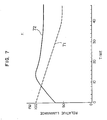
- Fig. 7 graphically illustrates the light emission characteristics of concern, wherein the time lapse from the lighting is taken along the abscissa with the relative luminances of the fluorescent lamp and the LED being taken along the ordinate.
- the relative luminance of the fluorescent lamp changes as indicated by a solid line curve 72, while that of the LED changes in such a manner as indicated by a broken line curve 71.
- a low temperature prevails immediately after the power-on of the LED and the fluorescent lamp. In this state, although the LED operates with a high emission efficiency, the fluorescent lamp is at a low output level.
- Fig. 8 shows an example of a colour separation reference table to be referred to upon discrimination or identification of colours.
- This table is so prepared that colours can be discriminatively identified in dependence on the signal level obtained under illumination by both the fluorescent lamp and the LED and the increment in the signal level (decrement in case the standardization illustrated in Fig. 5 is adopted).
- a number of such tables are prepared in consideration of the ratio in the quantity of light between the fluorescent lamp and the LED which ratio varies as a function of the temperature as described above, wherein the tables thus prepared are changed over from one to another so that correct colour identification can be realized constantly.
- FIG. 9A shows, by way of example, a signal obtained in the document reading operation based on a teaching of the present invention.
- a region 92 in a colour to serve as the reference for the colour separation is provided in a white plate 91 outside of the region where the document can be read.
- the reading operation is of course performed for the document.
- the white plate 91 is read for generating the shading waveform and other.
- reference numerals 93 and 95 designate signals resulting from reading of the white plate 91 and the reference colour 92, respectively, under illumination by both the fluorescent lamp and the LED array
- numerals 94 and 96 designates signals derived from the reading of the white plate 91 and the reference colour 92, respectively, under illumination only by the fluorescent lamp. It is possible to establish the criterion for the colour discrimination on the basis of the change in the level between the signals 95 and 96. Further, the curves 93 and 94 represent the shading waveforms under illumination with both the light sources and the fluorescent lamp alone, respectively. The detection of these signals can be achieved in the manner described hereinbefore.
- Fig. 10 shows an exemplary embodiment of a recorder of a monochromatic (white and black) facsimile equipment for recording the picture or video data sent thereto, being separated in two colours of red and black, in a monochromatic pattern.
- the region in black of the picture as received is printed in black dots over the whole region while the region in red is printed in black dots in a lattice-like pattern except for the boundary portion of the red region, as is illustrated in Fig. 11.
- a red region indicating circuit 105 With the black signal being furnished to a black region indicating circuit 106. Since the boundary is necessarily recorded in the black dots, data 109 to be recorded is supplied to a boundary detecting circuit 104.
- a lattice pattern generator 102 generates "1" and "0" signals alternately with a timing corresponding to the lattice constant.
- a reference numeral 101 denotes a colour commanding switch for commanding which of the red data or the black data is to be printed in the lattice pattern.
- a colour selector 103 connects the input thereto from the lattice pattern generator 102 to an output terminal 110 which is connected to one input terminal of a AND gate 114 for the red signal, resulting in that the AND gate 114 is enabled (on) and disabled (off) periodically at the interval corresponding to the lattice constant.
- one input of an AND gate 116 for the black signal is continuously supplied with the signal "1" from the other output terminal 112 of the colour selector 103, whereby the AND gate is continuously held in the on-state.
- the red signal supplied to the other input of the AND gate 114 for the red signal from the red region indicating circuit 105 is sent intermittently to the recorder 11 through the AND gate 114 and an OR gate 118, whereby the region originally in red is printed in the lattice pattern.
- the black signal applied to the other input of the AND gate 116 from the black region indicating circuit 106 is continuously transferred to the recorder 11 through the AND gate 116 and the OR gate 118, whereby the region originally in black is printed in the black dots of a high density.
- the red signal supplied to the red region indicating circuit 105 is applied to the boundary, detector 104, whereby portions of the data to be recorded corresponding to the leading end and the trailing end of the red signal, respectively, are extracted to be sent to the recorder 11 through the OR gate 118.
- the boundary is printed out without fail.
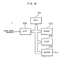
- FIG. 15 showing schematically system arrangement of the facsimile in terms of software
- two types of shading waveforms are previously stored in a memory 503 and loaded in a shading memory incorporated in a shading correction LSI-DIPP 502 of such structure as shown in Fig. 19 through a multiprocessing unit (MPU) 501.
- Picture or video data as inputted is coded by a coding/decoding LSI-DICEP 504 to be transmitted through a modem MODEM 505.
- Fig. 16 shows functionally another embodiment of the facsimile in which two shading correction LSI-DIPP 502′ and 502 ⁇ are used for storing previously different shading waveforms in the respective memories so that either one of two shading waveforms can be read out in the subsequent processing by the MPU 501. Except for this respect, the system arrangement shown in Fig. 16 is same as the one shown in Fig. 15.
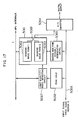
- Fig. 17 shows in a functional diagram still another embodiment of the invention according to which a plurality of shading memories are provided in view of the disadvantage of the prior system in which the shading correction LSI includes only one shading memory.
- the input signal 5068 from the image sensor 6 is applied to a peak hold circuit 5066 for the purpose of determining the quantity of light. More specifically, quantities of light under illumination by the different light sources (i.e. fluorescent lamp and LED), respectively, are held in the peak hold circuit 5066. On the basis of the quantities of light as placed in the peak hold circuit, the light quantity ratio is arithmetically determined by a light quantity ratio detecting circuit 5067, the result of which is messages to the MPU by way of a MPU interface bus.
- a shading waveform is derived from the input signal 5068 and loaded in the shading memory 5061 through a shading waveform storage/ regeneration control circuit 5065.
- the shading memory 5061 includes two waveform memories 5062 and 5063, for waveforms-1 and -2, respectively. By changing over these waveform memories by means of a change-over switch 5069, the corresponding shading waveform is supplied to an A/D converter 5064.
- Fig. 18 shows only functionally a facsimile system in which the LSI-DIPP 506 of the structure as the shading correction DIPP. Except for this differ lengthyence, the system structure is same as that shown in Fig. 15. It should however be noted that in the system shown in Fig. 18, the change-over of the shading wave-form is performed by the DIPP 506 itself without requiring any intervention of the MPU 501. Thus, significant improvement of the system performance can be assured.
- the LSI-DIPP for document data preprocessing is described in detail in JP-A-60-94576.
- the document data coding and decoding LSI-DIPP is described in detail in JP-A-56-126568. Accordingly, detailed description of these LSIs will be omitted here. For particulars, reference may be made to the abovementioned publications.
- An MTF correcting circuit 120 is provided for processing the black data 8 supplied from the distortion correcting unit 8.
- the gray region surrounding the character presents either white or black data, allowing the erroneous colour identification to be significantly suppressed.
- erroneous colour identification may often by made for the red region represented by the output signal of the colour separation circuit 9 when the red region is an isolated point.
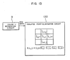
- Fig. 13 shows an isolated point eliminating circuit 130 provided with a view to excluding such erroneous colour identification.
- the processed red data f (i,j) is "0" even if the corresponding red data I i,j before being processed assumes the value of "1".
- the colour separation can be executed more reliably and stably.
Landscapes
- Engineering & Computer Science (AREA)
- Multimedia (AREA)
- Signal Processing (AREA)
- Facsimile Scanning Arrangements (AREA)
- Facsimile Image Signal Circuits (AREA)
- Color Image Communication Systems (AREA)
Applications Claiming Priority (2)
| Application Number | Priority Date | Filing Date | Title |
|---|---|---|---|
| JP51495/88 | 1988-03-07 | ||
| JP63051495A JPH06101796B2 (ja) | 1988-03-07 | 1988-03-07 | 多色読み取り装置及び多色フアクシミリ |
Publications (3)
| Publication Number | Publication Date |
|---|---|
| EP0332103A2 true EP0332103A2 (fr) | 1989-09-13 |
| EP0332103A3 EP0332103A3 (fr) | 1991-06-05 |
| EP0332103B1 EP0332103B1 (fr) | 1995-06-07 |
Family
ID=12888554
Family Applications (1)
| Application Number | Title | Priority Date | Filing Date |
|---|---|---|---|
| EP89103885A Expired - Lifetime EP0332103B1 (fr) | 1988-03-07 | 1989-03-06 | Appareil pour lire des documents en plusieurs couleurs pour fac-similé en plusieurs couleurs |
Country Status (4)
| Country | Link |
|---|---|
| US (1) | US4926253A (fr) |
| EP (1) | EP0332103B1 (fr) |
| JP (1) | JPH06101796B2 (fr) |
| DE (1) | DE68922923T2 (fr) |
Cited By (3)
| Publication number | Priority date | Publication date | Assignee | Title |
|---|---|---|---|---|
| US5245446A (en) * | 1990-10-10 | 1993-09-14 | Fuji Xerox Co., Ltd. | Image processing system |
| US6545771B1 (en) * | 1998-09-02 | 2003-04-08 | Sharp Kabushiki Kaisha | Facsimile apparatus and information printing method of facsimile apparatus |
| US6674926B1 (en) * | 1999-04-09 | 2004-01-06 | Eastman Kodak Company | Controller for a multiple array color sensor |
Families Citing this family (14)
| Publication number | Priority date | Publication date | Assignee | Title |
|---|---|---|---|---|
| JP2785274B2 (ja) * | 1988-07-07 | 1998-08-13 | ソニー株式会社 | カラー画像読取装置 |
| US5612792A (en) * | 1990-03-05 | 1997-03-18 | Canon Kabushiki Kaisha | Image processing method and apparatus for outputting a pattern image in accordance with the color and density level of each color of the output polychromatic image |
| JP3265429B2 (ja) * | 1990-09-14 | 2002-03-11 | キヤノン株式会社 | カラーファクシミリ装置 |
| JP3548205B2 (ja) | 1993-10-29 | 2004-07-28 | キヤノン株式会社 | 画像処理方法およびその装置 |
| CN1096790C (zh) * | 1995-02-24 | 2002-12-18 | 佳能株式会社 | 图象形成设备和光源装置 |
| US6330083B1 (en) * | 1997-05-28 | 2001-12-11 | Minolta Co., Ltd. | Image reading device performing light quantity detection and correction with timing corresponding to selected copying mode |
| JP2001177701A (ja) * | 1999-12-15 | 2001-06-29 | Nec Corp | 画像読取装置及び画像読取方法 |
| CN1264332C (zh) * | 2003-05-21 | 2006-07-12 | 致伸科技股份有限公司 | 可缩短扫描时间的扫描装置及相关方法 |
| JP2005065198A (ja) * | 2003-08-20 | 2005-03-10 | Ricoh Co Ltd | 画像形成装置および画像スキャン方法 |
| WO2006011450A1 (fr) * | 2004-07-29 | 2006-02-02 | Canon Components, Inc. | Dispositif de lecture d’image et méthode de lecture d’image |
| JP4537440B2 (ja) * | 2007-12-07 | 2010-09-01 | キヤノン株式会社 | 画像処理装置、画像処理方法、プログラム及び記録媒体 |
| US8432584B2 (en) * | 2007-12-26 | 2013-04-30 | Lexmark International, Inc. | Scanner and system employing composite illumination |
| JP5906889B2 (ja) * | 2012-03-29 | 2016-04-20 | 富士通株式会社 | 画像補正装置、画像補正方法、画像補正プログラム、及び画像読取装置 |
| JP6142815B2 (ja) * | 2014-02-13 | 2017-06-07 | ブラザー工業株式会社 | 画像読取装置 |
Family Cites Families (18)
| Publication number | Priority date | Publication date | Assignee | Title |
|---|---|---|---|---|
| DE3068810D1 (en) * | 1979-10-12 | 1984-09-06 | Xerox Corp | Apparatus and method for compensating a raster scanner for component deficiencies |
| JPS5666974A (en) * | 1979-11-02 | 1981-06-05 | Canon Inc | Picture forming method |
| JPS5979676A (ja) * | 1982-10-27 | 1984-05-08 | Canon Inc | 多色画像情報読み取り装置 |
| JPS59126368A (ja) * | 1983-01-10 | 1984-07-20 | Hitachi Ltd | 符号化復号化装置 |
| JPS59128872A (ja) * | 1983-01-14 | 1984-07-25 | Fuji Xerox Co Ltd | カラ−画情報処理装置 |
| JPS59189775A (ja) * | 1983-04-11 | 1984-10-27 | Fuji Xerox Co Ltd | カラ−画像読取方法および装置 |
| GB2138244B (en) * | 1983-04-11 | 1987-03-11 | Fuji Xerox Co Ltd | Method and apparatus for reading color image |
| JPS6038972A (ja) * | 1983-08-11 | 1985-02-28 | Toshiba Corp | 入力表示装置 |
| JPH0738682B2 (ja) * | 1983-10-28 | 1995-04-26 | 株式会社日立製作所 | 画像信号処理プロセツサ |
| GB2159016B (en) * | 1984-05-10 | 1987-12-02 | Dainippon Screen Mfg | Image data correction |
| JPS6174447A (ja) * | 1984-09-20 | 1986-04-16 | Toshiba Corp | シエ−デイング補正回路 |
| JPS61191168A (ja) * | 1985-02-20 | 1986-08-25 | Fuji Xerox Co Ltd | カラ−画像読取装置 |
| DE3605696A1 (de) * | 1985-02-21 | 1986-08-21 | Fuji Photo Film Co., Ltd., Minami-Ashigara, Kanagawa | Bildausleseverfahren und bildauslesevorrichtung |
| JPS61206367A (ja) * | 1985-03-11 | 1986-09-12 | Hitachi Ltd | カラ−信号色処理回路 |
| JPS6291068A (ja) * | 1985-10-17 | 1987-04-25 | Canon Inc | カラ−原稿読取り装置 |
| JPS62165479A (ja) * | 1986-01-17 | 1987-07-22 | Hitachi Ltd | 複数色フアクシミリ |
| JPS62174824A (ja) * | 1986-01-29 | 1987-07-31 | Hitachi Ltd | 画面表示情報の印字方法 |
| DE3778602D1 (de) * | 1986-07-18 | 1992-06-04 | Dainippon Screen Mfg | Bild-datenverarbeitungsverfahren und anordnung dafuer. |
-
1988
- 1988-03-07 JP JP63051495A patent/JPH06101796B2/ja not_active Expired - Lifetime
-
1989
- 1989-03-06 US US07/319,970 patent/US4926253A/en not_active Expired - Lifetime
- 1989-03-06 DE DE68922923T patent/DE68922923T2/de not_active Expired - Fee Related
- 1989-03-06 EP EP89103885A patent/EP0332103B1/fr not_active Expired - Lifetime
Cited By (3)
| Publication number | Priority date | Publication date | Assignee | Title |
|---|---|---|---|---|
| US5245446A (en) * | 1990-10-10 | 1993-09-14 | Fuji Xerox Co., Ltd. | Image processing system |
| US6545771B1 (en) * | 1998-09-02 | 2003-04-08 | Sharp Kabushiki Kaisha | Facsimile apparatus and information printing method of facsimile apparatus |
| US6674926B1 (en) * | 1999-04-09 | 2004-01-06 | Eastman Kodak Company | Controller for a multiple array color sensor |
Also Published As
| Publication number | Publication date |
|---|---|
| DE68922923T2 (de) | 1995-11-23 |
| US4926253A (en) | 1990-05-15 |
| JPH06101796B2 (ja) | 1994-12-12 |
| DE68922923D1 (de) | 1995-07-13 |
| EP0332103A3 (fr) | 1991-06-05 |
| EP0332103B1 (fr) | 1995-06-07 |
| JPH01226276A (ja) | 1989-09-08 |
Similar Documents
| Publication | Publication Date | Title |
|---|---|---|
| EP0332103B1 (fr) | Appareil pour lire des documents en plusieurs couleurs pour fac-similé en plusieurs couleurs | |
| EP0809392B1 (fr) | Appareil et unité d'analyse d'images et appareil de commande | |
| US5371610A (en) | Image data processing apparatus | |
| US5751446A (en) | Image reading device for accurately reading spread pages of a book document | |
| JPH08172532A (ja) | 画像読み取り装置および読み取り方法 | |
| JPH1170780A (ja) | 電子黒板装置 | |
| US6798544B1 (en) | Image reading method, image reading device and image processing device | |
| US20060227392A1 (en) | Image reading apparatus | |
| US6055007A (en) | Image processing device and image reading device | |
| US20050128522A1 (en) | Counterfeiting instrument tracking high speed color printing apparatus | |
| US5592303A (en) | Image communication apparatus and method which extracts and records images on the transmission side | |
| JPH0380668A (ja) | 高品質イメージスキャナー | |
| JP3289965B2 (ja) | 赤黒読取装置 | |
| JPS62219766A (ja) | 画像処理装置 | |
| JP3168020B2 (ja) | 画像読取装置および方法 | |
| JP3411791B2 (ja) | 画像読取装置 | |
| JP2656561B2 (ja) | カラー画像処理装置 | |
| JP2557481B2 (ja) | カラー画像処理装置 | |
| JP2000083134A (ja) | カラー読み取り装置、カラー読み取り方法、カラーファクシミリ装置、カラーコピー装置及び記憶媒体 | |
| JPH07264406A (ja) | 画像読取装置のガンマ補正方法 | |
| JPH02121471A (ja) | 画像読取装置 | |
| JPH02274063A (ja) | 画像読取装置 | |
| JP2002185781A (ja) | 画像読み取り装置 | |
| JPH0425284A (ja) | 画像読取装置 | |
| JP2000032279A (ja) | 画像読取装置 |
Legal Events
| Date | Code | Title | Description |
|---|---|---|---|
| PUAI | Public reference made under article 153(3) epc to a published international application that has entered the european phase |
Free format text: ORIGINAL CODE: 0009012 |
|
| 17P | Request for examination filed |
Effective date: 19890306 |
|
| AK | Designated contracting states |
Kind code of ref document: A2 Designated state(s): DE FR GB |
|
| PUAL | Search report despatched |
Free format text: ORIGINAL CODE: 0009013 |
|
| AK | Designated contracting states |
Kind code of ref document: A3 Designated state(s): DE FR GB |
|
| 17Q | First examination report despatched |
Effective date: 19930722 |
|
| GRAA | (expected) grant |
Free format text: ORIGINAL CODE: 0009210 |
|
| AK | Designated contracting states |
Kind code of ref document: B1 Designated state(s): DE FR GB |
|
| REF | Corresponds to: |
Ref document number: 68922923 Country of ref document: DE Date of ref document: 19950713 |
|
| ET | Fr: translation filed | ||
| PLBE | No opposition filed within time limit |
Free format text: ORIGINAL CODE: 0009261 |
|
| STAA | Information on the status of an ep patent application or granted ep patent |
Free format text: STATUS: NO OPPOSITION FILED WITHIN TIME LIMIT |
|
| 26N | No opposition filed | ||
| REG | Reference to a national code |
Ref country code: GB Ref legal event code: IF02 |
|
| PGFP | Annual fee paid to national office [announced via postgrant information from national office to epo] |
Ref country code: FR Payment date: 20020228 Year of fee payment: 14 |
|
| PGFP | Annual fee paid to national office [announced via postgrant information from national office to epo] |
Ref country code: GB Payment date: 20020301 Year of fee payment: 14 |
|
| PGFP | Annual fee paid to national office [announced via postgrant information from national office to epo] |
Ref country code: DE Payment date: 20020328 Year of fee payment: 14 |
|
| PG25 | Lapsed in a contracting state [announced via postgrant information from national office to epo] |
Ref country code: GB Free format text: LAPSE BECAUSE OF NON-PAYMENT OF DUE FEES Effective date: 20030306 |
|
| PG25 | Lapsed in a contracting state [announced via postgrant information from national office to epo] |
Ref country code: DE Free format text: LAPSE BECAUSE OF NON-PAYMENT OF DUE FEES Effective date: 20031001 |
|
| GBPC | Gb: european patent ceased through non-payment of renewal fee |
Effective date: 20030306 |
|
| PG25 | Lapsed in a contracting state [announced via postgrant information from national office to epo] |
Ref country code: FR Free format text: LAPSE BECAUSE OF NON-PAYMENT OF DUE FEES Effective date: 20031127 |
|
| REG | Reference to a national code |
Ref country code: FR Ref legal event code: ST |