EP0365854A2 - Dispositif semi-conducteur comprenant une structure conductrice multi-couche - Google Patents
Dispositif semi-conducteur comprenant une structure conductrice multi-couche Download PDFInfo
- Publication number
- EP0365854A2 EP0365854A2 EP89117848A EP89117848A EP0365854A2 EP 0365854 A2 EP0365854 A2 EP 0365854A2 EP 89117848 A EP89117848 A EP 89117848A EP 89117848 A EP89117848 A EP 89117848A EP 0365854 A2 EP0365854 A2 EP 0365854A2
- Authority
- EP
- European Patent Office
- Prior art keywords
- film
- insulating film
- semiconductor device
- metal wiring
- plasma cvd
- Prior art date
- Legal status (The legal status is an assumption and is not a legal conclusion. Google has not performed a legal analysis and makes no representation as to the accuracy of the status listed.)
- Ceased
Links
Images

Classifications
-
- H—ELECTRICITY
- H10—SEMICONDUCTOR DEVICES; ELECTRIC SOLID-STATE DEVICES NOT OTHERWISE PROVIDED FOR
- H10W—GENERIC PACKAGES, INTERCONNECTIONS, CONNECTORS OR OTHER CONSTRUCTIONAL DETAILS OF DEVICES COVERED BY CLASS H10
- H10W20/00—Interconnections in chips, wafers or substrates
- H10W20/01—Manufacture or treatment
- H10W20/031—Manufacture or treatment of conductive parts of the interconnections
-
- H—ELECTRICITY
- H10—SEMICONDUCTOR DEVICES; ELECTRIC SOLID-STATE DEVICES NOT OTHERWISE PROVIDED FOR
- H10W—GENERIC PACKAGES, INTERCONNECTIONS, CONNECTORS OR OTHER CONSTRUCTIONAL DETAILS OF DEVICES COVERED BY CLASS H10
- H10W20/00—Interconnections in chips, wafers or substrates
- H10W20/40—Interconnections external to wafers or substrates, e.g. back-end-of-line [BEOL] metallisations or vias connecting to gate electrodes
- H10W20/45—Interconnections external to wafers or substrates, e.g. back-end-of-line [BEOL] metallisations or vias connecting to gate electrodes characterised by their insulating parts
- H10W20/48—Insulating materials thereof
-
- H—ELECTRICITY
- H10—SEMICONDUCTOR DEVICES; ELECTRIC SOLID-STATE DEVICES NOT OTHERWISE PROVIDED FOR
- H10P—GENERIC PROCESSES OR APPARATUS FOR THE MANUFACTURE OR TREATMENT OF DEVICES COVERED BY CLASS H10
- H10P14/00—Formation of materials, e.g. in the shape of layers or pillars
- H10P14/60—Formation of materials, e.g. in the shape of layers or pillars of insulating materials
- H10P14/63—Formation of materials, e.g. in the shape of layers or pillars of insulating materials characterised by the formation processes
- H10P14/6326—Deposition processes
- H10P14/6328—Deposition from the gas or vapour phase
- H10P14/6334—Deposition from the gas or vapour phase using decomposition or reaction of gaseous or vapour phase compounds, i.e. chemical vapour deposition
- H10P14/6336—Deposition from the gas or vapour phase using decomposition or reaction of gaseous or vapour phase compounds, i.e. chemical vapour deposition in the presence of a plasma [PECVD]
-
- H—ELECTRICITY
- H10—SEMICONDUCTOR DEVICES; ELECTRIC SOLID-STATE DEVICES NOT OTHERWISE PROVIDED FOR
- H10W—GENERIC PACKAGES, INTERCONNECTIONS, CONNECTORS OR OTHER CONSTRUCTIONAL DETAILS OF DEVICES COVERED BY CLASS H10
- H10W20/00—Interconnections in chips, wafers or substrates
- H10W20/40—Interconnections external to wafers or substrates, e.g. back-end-of-line [BEOL] metallisations or vias connecting to gate electrodes
- H10W20/45—Interconnections external to wafers or substrates, e.g. back-end-of-line [BEOL] metallisations or vias connecting to gate electrodes characterised by their insulating parts
- H10W20/47—Interconnections external to wafers or substrates, e.g. back-end-of-line [BEOL] metallisations or vias connecting to gate electrodes characterised by their insulating parts comprising two or more dielectric layers having different properties, e.g. different dielectric constants
Definitions
- the present invention relates to a semiconductor device having a multi-layered wiring structure.
- an insulating film is formed to have a laminated film structure comprising an SiO2 film or SiON film, formed by an ordinary plasma CVD method which generally provides a high productivity, and a film formed by the substrate-bias applying method, in consideration of reducing the leak current of the thin film (the leak current being more than 100 times that of an SiO2 film formed by an ordinary plasma CVD method (at a measuring temperature of about 200°C)) and improving the productivity.
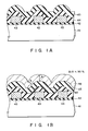
- Figs. 1A and 1B illustrate an example of a conventional multi-layered wiring structure.
- a first insulating film 44 and a second insulating film 45 are deposited on first metal wiring layers 43 formed on a thermal oxide film 42 on a semiconductor substrate 41 (Fig. 1A).
- the layer 44 is formed by the substrate-bias applying method, and the layer 45 by the ordinary plasma CVD method.
- a second metal wiring layer 46 is formed on the second insulating film 46 (Fig. 1B).
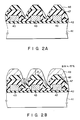
- Figs. 2A and 2B illustrate another example of the multi-layered wiring structure.
- a first insulating film 47 and a second insulating film 48 are deposited on the first metal wiring layers 43 by the ordinary plasma CVD method and the substrate-bias applying method, respectively (Fig. 2A).
- a second metal wiring layer 49 is formed on the second insulating film 48 (Fig. 2B).
- the positive-ion sputtering/etching effect produced by applying a bias to the substrate are utilized in forming the first insulating film 44 for film flattening. Therefore, a defect is likely to occur on the surface or bulk of the first metal wiring layers 43. Since this defect would cause a stress migration or electromigration, thus resulting in disconnection of the first metal wiring layers 43, it directly influences the reliability of a semiconductor device. In the example shown in Figs. 2A and 2B, although this defect which may occur in the first example, can be avoided, there is insufficient step coverage of the first insulating film 47 at the stepped portion of each first metal wiring layer 43.
- the conventional semiconductor devices cannot satisfy both improvement of the reliability of the first metal wiring layers and the flattening effect produced by an insulating film.
- an object of this invention to provide a semiconductor device in which an interlayer insulating film in a multi-layered wiring structure can be formed with a high productivity and with a film flattening effect, without reducing the reliability of the first metal wiring layers.
- the interlayer insulating film in the multi-layered wiring structure is formed as thin as 500 to 3000 ⁇ by the first insulating film formed in contact with the surface of the first metal wiring layers, such as an SiO2 film, SiON film, or Si3N4 film, formed by the plasma CVD method, or a PSG film, LTO film, spin-on-glass film or polyimide film.
- the second insulating film is deposited on the first insulating film by the substrate-bias applying method to flatten the interlayer insulating film.
- the third insulating film is further deposited on the second insulating film by the same method as used for forming the first insulating film, in order to improve the productivity.
- the first insulating film protects the first metal wiring layers, the first metal wiring layers will not be damaged if the second insulating film is deposited on the first insulating film by the substrate-bias applying method.
- the deposition of the third insulating film on the second insulating film improves the productivity.
- the second insulating film is flat, the third insulating film can also be formed flat, thus making the overall interlayer insulating film flat.
- Figs. 3A and 3B are illustrate the cross sections of a semiconductor device embodying the present invention.
- a thermal oxide film 2 and first metal wiring layers 3a-3c are formed on a semiconductor substrate 1 as per the conventional device.
- An SiO2 film 4 serving as a protection film to protect the first metal wiring layers, is deposited on the first metal wiring layers 3a-3c by the ordinary plasma CVD method.
- Another SiO2 film 5 is deposited on this film 4 by the bias sputtering method.
- An SiO2 film 6 is further deposited on the film 5 by the ordinary plasma CVD method (see Fig. 3A).
- a second metal wiring layer 7 is formed on the SiO2 film 6 by the sputtering method (see Fig. 3B).
- the best thickness of the SiO2 film 4 as the wiring protection film would be 500 to 3000 ⁇ .
- the first metal wiring layers 3a-3c are formed of Al or Al alloy, an SiO2 film, SiON film, or Si3N4 film, formed by the plasma CVD method, or a PSG film, LTO film, spin-on-glass film or polyimide film is used as the wiring protection film.
- the interlayer insulating film is formed only by the SiO2 film 5 using the bias sputtering method after forming the wiring protection film, it takes time to produce a semiconductor device and it is therefore impractical. If the interlayer insulating film is formed to have a laminated structure of the SiO2 film 5 and the SiO2 film 6, formed by the ordinary plasma CVD method which yields a high productivity, the productivity of the semiconductor devices can be improved while reducing the leak current.
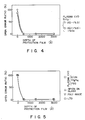
- a semiconductor device according to the present invention was produced and some power-on tests were conducted to evaluate the reliability of the metal wiring layers 3.
- SiO2 films 4 respectively having thicknesses of 500 ⁇ , 1500 ⁇ and 3000 ⁇ were prepared.
- the SiO2 film 5 of approximately 8000 ⁇ was deposited on this SiO2 film 4 using the bias sputtering method, and the SiO2 film 6 of 8000 ⁇ was deposited on this SiO2 film 5 using the ordinary plasma CVD method.
- An Al-1 wt.% Si film of about 1.0 ⁇ m thickness serving as the second metal wiring layer 7 was formed on the SiO2 film 6 by the sputtering method.
- the disconnection defect rate is 0 % for the protection film having a thickness of 500 ⁇ or above. This means that no disconnection defect due to electromigration or stress migration had occurred in either the Al-1 wt.% Si film or Al-1 wt.% Si-1 wt.% Cu film. It was found that the step coverage of the protection film at the stepped portion of each first metal wiring layer 3 is satisfactory within a range of 500 to 3000 ⁇ .
- the same power-on test was conducted using an SiO2 film, SiON film, or Si3N4 film, formed by the plasma CVD method, or a PSG film, LTO film, spin-on-glass film or polyimide film as the protection film on the first metal wiring layers 3a-3c comprising an Al-1 wt.% Si film. It was confirmed as shown in Fig. 5 that the same effects as produced by using the SiO2 film 4, formed by the plasma CVD method, as the protection film.
- the substrate-bias applying method instead of the bias sputtering method may be used as a method to form an insulating film having the film flattening effect.
- the present invention can apply to an interlayer insulating film formed between the second metal wiring layer 7 and the third metal wiring layer on the layer 7, when such is a case.
- the present invention is effective in forming an interlayer insulating film between wiring layers in a multi-layered wiring structure.
Landscapes
- Internal Circuitry In Semiconductor Integrated Circuit Devices (AREA)
Applications Claiming Priority (2)
| Application Number | Priority Date | Filing Date | Title |
|---|---|---|---|
| JP63241518A JPH0289346A (ja) | 1988-09-27 | 1988-09-27 | 半導体装置及びその製造方法 |
| JP241518/88 | 1988-09-27 |
Publications (2)
| Publication Number | Publication Date |
|---|---|
| EP0365854A2 true EP0365854A2 (fr) | 1990-05-02 |
| EP0365854A3 EP0365854A3 (fr) | 1990-12-05 |
Family
ID=17075537
Family Applications (1)
| Application Number | Title | Priority Date | Filing Date |
|---|---|---|---|
| EP19890117848 Ceased EP0365854A3 (fr) | 1988-09-27 | 1989-09-27 | Dispositif semi-conducteur comprenant une structure conductrice multi-couche |
Country Status (3)
| Country | Link |
|---|---|
| EP (1) | EP0365854A3 (fr) |
| JP (1) | JPH0289346A (fr) |
| KR (1) | KR930004981B1 (fr) |
Cited By (6)
| Publication number | Priority date | Publication date | Assignee | Title |
|---|---|---|---|---|
| DE4032099A1 (de) * | 1990-10-08 | 1992-04-16 | Gold Star Electronics | Dram-bauteil und verfahren zu seiner herstellung |
| DE4133625A1 (de) * | 1990-12-19 | 1992-07-02 | Samsung Electronics Co Ltd | Halbleiter-umschmelzverfahren |
| EP0689246A1 (fr) * | 1994-05-27 | 1995-12-27 | Texas Instruments Incorporated | Améliorations concernant des dispositifs semi-conducteurs |
| EP0706216A3 (fr) * | 1994-10-03 | 1997-12-03 | Sony Corporation | Couche intermédiaire diélectrique pour un dispositif semi-conducteur |
| US5786624A (en) * | 1994-06-07 | 1998-07-28 | Texas Instruments Incorporated | Dual masking for selective gap fill of submicron interconnects |
| US6133163A (en) * | 1994-07-29 | 2000-10-17 | Texas Instruments Incorporated | Method for forming a semiconductor multilayer interconnect device using SOG and polyimide |
Families Citing this family (5)
| Publication number | Priority date | Publication date | Assignee | Title |
|---|---|---|---|---|
| JP3010824B2 (ja) * | 1991-09-17 | 2000-02-21 | 株式会社日立製作所 | 半導体装置及びその製造方法 |
| JPH09321047A (ja) * | 1996-05-24 | 1997-12-12 | Nec Corp | 半導体装置の製造方法 |
| JPH10163192A (ja) * | 1996-10-03 | 1998-06-19 | Fujitsu Ltd | 半導体装置およびその製造方法 |
| JP2005101597A (ja) * | 2003-09-04 | 2005-04-14 | Seiko Epson Corp | 半導体装置およびその製造方法 |
| US20170066684A1 (en) * | 2015-09-08 | 2017-03-09 | Corning Incorporated | Optical coatings including buffer layers |
Family Cites Families (7)
| Publication number | Priority date | Publication date | Assignee | Title |
|---|---|---|---|---|
| JPS5289468A (en) * | 1976-01-21 | 1977-07-27 | Hitachi Ltd | Semiconductor device |
| US4273805A (en) * | 1978-06-19 | 1981-06-16 | Rca Corporation | Passivating composite for a semiconductor device comprising a silicon nitride (Si1 3N4) layer and phosphosilicate glass (PSG) layer |
| JPS58197824A (ja) * | 1982-05-14 | 1983-11-17 | Hitachi Ltd | 半導体装置 |
| JPS5957456A (ja) * | 1982-09-27 | 1984-04-03 | Fujitsu Ltd | 半導体装置の製造方法 |
| EP0177845A1 (fr) * | 1984-09-28 | 1986-04-16 | Siemens Aktiengesellschaft | Circuit intégré à métallisation multicouche et procédé pour sa fabrication |
| US4723197A (en) * | 1985-12-16 | 1988-02-02 | National Semiconductor Corporation | Bonding pad interconnection structure |
| JPH01138734A (ja) * | 1987-11-25 | 1989-05-31 | Mitsubishi Electric Corp | 複導電体層を有する半導体装置およびその製造方法 |
-
1988
- 1988-09-27 JP JP63241518A patent/JPH0289346A/ja active Granted
-
1989
- 1989-09-27 EP EP19890117848 patent/EP0365854A3/fr not_active Ceased
- 1989-09-27 KR KR1019890013911A patent/KR930004981B1/ko not_active Expired - Fee Related
Cited By (8)
| Publication number | Priority date | Publication date | Assignee | Title |
|---|---|---|---|---|
| DE4032099A1 (de) * | 1990-10-08 | 1992-04-16 | Gold Star Electronics | Dram-bauteil und verfahren zu seiner herstellung |
| DE4133625A1 (de) * | 1990-12-19 | 1992-07-02 | Samsung Electronics Co Ltd | Halbleiter-umschmelzverfahren |
| EP0689246A1 (fr) * | 1994-05-27 | 1995-12-27 | Texas Instruments Incorporated | Améliorations concernant des dispositifs semi-conducteurs |
| US5751066A (en) * | 1994-05-27 | 1998-05-12 | Texas Instruments Incorporated | Structure with selective gap fill of submicron interconnects |
| US5786624A (en) * | 1994-06-07 | 1998-07-28 | Texas Instruments Incorporated | Dual masking for selective gap fill of submicron interconnects |
| US5789319A (en) * | 1994-06-07 | 1998-08-04 | Texas Instruments Incorporated | Method of dual masking for selective gap fill of submicron interconnects |
| US6133163A (en) * | 1994-07-29 | 2000-10-17 | Texas Instruments Incorporated | Method for forming a semiconductor multilayer interconnect device using SOG and polyimide |
| EP0706216A3 (fr) * | 1994-10-03 | 1997-12-03 | Sony Corporation | Couche intermédiaire diélectrique pour un dispositif semi-conducteur |
Also Published As
| Publication number | Publication date |
|---|---|
| EP0365854A3 (fr) | 1990-12-05 |
| JPH0576187B2 (fr) | 1993-10-22 |
| KR900005593A (ko) | 1990-04-14 |
| KR930004981B1 (ko) | 1993-06-11 |
| JPH0289346A (ja) | 1990-03-29 |
Similar Documents
| Publication | Publication Date | Title |
|---|---|---|
| US5470793A (en) | Method of via formation for the multilevel interconnect integrated circuits | |
| US4244002A (en) | Semiconductor device having bump terminal electrodes | |
| EP0365854A2 (fr) | Dispositif semi-conducteur comprenant une structure conductrice multi-couche | |
| EP0318954A2 (fr) | Dispositif semi-conducteur comprenant une couche intermédiaire composée en matière isolante | |
| US4495222A (en) | Metallization means and method for high temperature applications | |
| US4600658A (en) | Metallization means and method for high temperature applications | |
| US5962920A (en) | Semiconductor device and a manufacturing method thereof | |
| JPS60145628A (ja) | 半導体装置 | |
| JPH10189590A (ja) | 半導体装置及びその製造方法 | |
| JPH04731A (ja) | 半導体装置及びその製造方法 | |
| JP3230909B2 (ja) | 半導体装置およびその製造方法 | |
| JPH0332214B2 (fr) | ||
| JP2760061B2 (ja) | 半導体装置の製造方法 | |
| JPS60103668A (ja) | 半導体装置 | |
| JP2917362B2 (ja) | 半導体装置の製造方法 | |
| JPH02117154A (ja) | 半導体装置の製造方法 | |
| JPH02271628A (ja) | 半導体装置 | |
| JPS60160144A (ja) | バンプ形成方法 | |
| JPS61193469A (ja) | 半導体装置の製造方法 | |
| JPH056939A (ja) | 半導体装置の製造方法 | |
| JPS6058621A (ja) | 化合物半導体素子の電極の製造方法 | |
| JPH05304219A (ja) | 半導体装置における絶縁層の形成方法 | |
| JPS63211743A (ja) | 半導体装置 | |
| JPH04186729A (ja) | 半導体装置 | |
| JPH0258228A (ja) | 半導体集積回路 |
Legal Events
| Date | Code | Title | Description |
|---|---|---|---|
| PUAI | Public reference made under article 153(3) epc to a published international application that has entered the european phase |
Free format text: ORIGINAL CODE: 0009012 |
|
| 17P | Request for examination filed |
Effective date: 19890927 |
|
| AK | Designated contracting states |
Kind code of ref document: A2 Designated state(s): DE FR GB |
|
| PUAL | Search report despatched |
Free format text: ORIGINAL CODE: 0009013 |
|
| AK | Designated contracting states |
Kind code of ref document: A3 Designated state(s): DE FR GB |
|
| 17Q | First examination report despatched |
Effective date: 19931119 |
|
| STAA | Information on the status of an ep patent application or granted ep patent |
Free format text: STATUS: THE APPLICATION HAS BEEN REFUSED |
|
| 18R | Application refused |
Effective date: 19960425 |