EP0376847A2 - Synthétiseur à PLL - Google Patents
Synthétiseur à PLL Download PDFInfo
- Publication number
- EP0376847A2 EP0376847A2 EP89403666A EP89403666A EP0376847A2 EP 0376847 A2 EP0376847 A2 EP 0376847A2 EP 89403666 A EP89403666 A EP 89403666A EP 89403666 A EP89403666 A EP 89403666A EP 0376847 A2 EP0376847 A2 EP 0376847A2
- Authority
- EP
- European Patent Office
- Prior art keywords
- signal
- pll
- frequency
- pll synthesizer
- supplied
- Prior art date
- Legal status (The legal status is an assumption and is not a legal conclusion. Google has not performed a legal analysis and makes no representation as to the accuracy of the status listed.)
- Granted
Links
Images




Classifications
-
- H—ELECTRICITY
- H03—ELECTRONIC CIRCUITRY
- H03L—AUTOMATIC CONTROL, STARTING, SYNCHRONISATION OR STABILISATION OF GENERATORS OF ELECTRONIC OSCILLATIONS OR PULSES
- H03L7/00—Automatic control of frequency or phase; Synchronisation
- H03L7/06—Automatic control of frequency or phase; Synchronisation using a reference signal applied to a frequency- or phase-locked loop
- H03L7/16—Indirect frequency synthesis, i.e. generating a desired one of a number of predetermined frequencies using a frequency- or phase-locked loop
- H03L7/18—Indirect frequency synthesis, i.e. generating a desired one of a number of predetermined frequencies using a frequency- or phase-locked loop using a frequency divider or counter in the loop
- H03L7/183—Indirect frequency synthesis, i.e. generating a desired one of a number of predetermined frequencies using a frequency- or phase-locked loop using a frequency divider or counter in the loop a time difference being used for locking the loop, the counter counting between fixed numbers or the frequency divider dividing by a fixed number
-
- H—ELECTRICITY
- H03—ELECTRONIC CIRCUITRY
- H03L—AUTOMATIC CONTROL, STARTING, SYNCHRONISATION OR STABILISATION OF GENERATORS OF ELECTRONIC OSCILLATIONS OR PULSES
- H03L7/00—Automatic control of frequency or phase; Synchronisation
- H03L7/06—Automatic control of frequency or phase; Synchronisation using a reference signal applied to a frequency- or phase-locked loop
- H03L7/08—Details of the phase-locked loop
- H03L7/10—Details of the phase-locked loop for assuring initial synchronisation or for broadening the capture range
- H03L7/107—Details of the phase-locked loop for assuring initial synchronisation or for broadening the capture range using a variable transfer function for the loop, e.g. low pass filter having a variable bandwidth
- H03L7/1075—Details of the phase-locked loop for assuring initial synchronisation or for broadening the capture range using a variable transfer function for the loop, e.g. low pass filter having a variable bandwidth by changing characteristics of the loop filter, e.g. changing the gain, changing the bandwidth
-
- H—ELECTRICITY
- H03—ELECTRONIC CIRCUITRY
- H03L—AUTOMATIC CONTROL, STARTING, SYNCHRONISATION OR STABILISATION OF GENERATORS OF ELECTRONIC OSCILLATIONS OR PULSES
- H03L7/00—Automatic control of frequency or phase; Synchronisation
- H03L7/06—Automatic control of frequency or phase; Synchronisation using a reference signal applied to a frequency- or phase-locked loop
- H03L7/08—Details of the phase-locked loop
- H03L7/085—Details of the phase-locked loop concerning mainly the frequency- or phase-detection arrangement including the filtering or amplification of its output signal
- H03L7/089—Details of the phase-locked loop concerning mainly the frequency- or phase-detection arrangement including the filtering or amplification of its output signal the phase or frequency detector generating up-down pulses
- H03L7/0891—Details of the phase-locked loop concerning mainly the frequency- or phase-detection arrangement including the filtering or amplification of its output signal the phase or frequency detector generating up-down pulses the up-down pulses controlling source and sink current generators, e.g. a charge pump
Definitions
- the present invention generally relates to a PLL synthesizer, and more particularly to a PLL synthesizer which controls the frequency of an output signal so as to be always equal to a desired frequency.
- the present invention is suitable for a digital tuner, for example.
- a PLL (phase-locked loop) synthesizer is a feedback circuit which functions to make the frequency of an output signal equal to a desired frequency.
- a lowpass filter is provided in the PLL loop to improve the purity of the output signal derived from the PLL synthesizer.
- the desired frequency is changed to a different frequency, it takes a lock-up time the frequency of the PLL synthesizer to be settled at the different frequency.
- FIG.1 is a block diagram of a conventional PLL synthesizer.
- the PLL synthesizer is supplied with a clock signal CK, set frequency data DA, and a strobe signal STB, all of which are derived from an external circuit (not shown).
- the strobe signal STB is supplied to the PLL synthesizer while the set frequency data DA is being input thereto, the set frequency data DA is written into a PLL operation circuit 1 in synchronism with the clock signal CK.
- the PLL operation circuit 1 divides the set frequency data DA on the basis of a reference frequency generated by a crystal oscillator 2 and thereby generates a set signal fr, which is supplied to a phase comparator 3.
- the PLL operation circuit 1 is supplied with a signal supplied from a prescaler circuit (frequency divider) 7.
- the signal from the prescaler circuit 7 is frequency-divided by the PLL operation circuit 1 so that a feedback signal fp to be supplied to the phase comparator 3 is generated.
- the phase comparator 3 generates pulse signals ⁇ r and ⁇ p which are based on the frequencies of the set signal fr and the feedback signal fp as well as the phase difference therebetween as shown in (A) and (B) of FIG.2.
- the charge pump circuit 4 derives a signal SG1 as shown in (C) of FIG.2 from the pulse signals ⁇ r and ⁇ p.
- the signal SG1 contains pulse components on a DC component thereof. This DC component of the signal SG1 is increased or decreased in response to fluctuations of the frequencies of the pulse signals ⁇ r and ⁇ p.
- the pulse components contained in the signal SG1 are varied on the basis of the phase difference between the pulse signals ⁇ r and ⁇ p.
- the lowpass filter 5 smooths the signal SG1 derived from the charge pump circuit 4 and eliminates the pulse components from the signal SG1. Thereby, a signal SG2 having no pulse components is generated by the lowpass filter 5.
- the signal thus formed is supplied to a voltage-controlled oscillator (hereinafter simply referred to as a VCO) 6, which generates an output signal SG3 having a frequency based on the voltage of the signal SG2 supplied from the lowpass filter 5.
- the output signal SG3 is supplied to the prescaler circuit 7, which divides the frequency of the output signal SG3.
- the signal derived from the prescaler circuit 7 is further frequency-divided by the PLL operation circuit 1 so that the aforementioned feedback signal fp is generated.
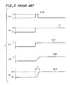
- the PLL synthesizer shown in FIG.1 operates as shown in FIG.3.
- the frequency fr1 of the set signal fr output from the PLL operation circuit 1 is increased to a frequency fr2 as shown in (B) of FIG.3.
- the DC component of the signal SG1 output from the charge pump circuit 4 is increased, and the voltage of the signal SG2 is also increased as shown in (D) of FIG.3.
- the frequency of the output signal SG3 derived from the VCO 6 is changed from the frequency F1 to the frequency F2 as shown in (E) of FIG.3.
- the output signal SG3 is always fed back to the PLL operation circuit 1 through the prescaler circuit 7.
- the frequency of the feedback signal fp is adjusted so as to become equal to the frequency fr2.
- the PLL synthesizer can generate different frequencies by the use of a single crystal oscillator 2 with a stability approximately equal to that for the crystal oscillator 2. It is noted that the pulse components contained in the signal SG1 shown in (C) of FIG.3 are omitted for the convenience' sake.
- the aforementioned PLL synthesizer has disadvantages as described below.
- the signal output from the charge pump circuit 4 is supplied to the VCO 6 through the lowpass filter 5.
- the PLL synthesizer needs a lock-up time t1 (FIG.3-(E)) based on a time constant of the lowpass filter 5 until the frequency of the output signal SG3 is settled at the revised frequency F2 after the DC level of the output signal SG1 starts changing.
- the PLL synthesizer shown in FIG.1 is applied to a digital tuner, tuning is not available during the lock-up time t1 and a noise is introduced in the output signal SG3.
- the pulse component contained in the signal SG1 derived from the charge pump circuit 4 is applied to the VCO 6 without being eliminated. This causes a deterioration of the output signal SG3 and degrades the purity of the output signal SG3.
- a more specific object of the present invention is to provide a PLL synthesizer having a reduced lock-up time.
- a PLL synthesizer comprising a voltage-controlled oscillator generating an output signal having a frequency based on a first signal supplied thereto; PLL controlling means for generating a second signal based on the the output signal and a desired set frequency; lowpass filter means having an input terminal and an output terminal, for filtering the second signal supplied through the input terminal to thereby generate the first signal supplied to the voltage-controlled oscillator through the output terminal; and switch means, coupled between the input and output terminals of the lowpass filter means, for supplying the second signal directly to the voltage-controlled oscillator during a predetermined time when the desired set frequency is changed.
- a PLL synthesizer comprising a voltage-controlled oscillator generating an output signal having a frequency based on a first signal supplied thereto; PLL controlling means for generating a second signal based on the the output signal and a desired set frequency; first lowpass filter means having an input terminal and an output terminal, for filtering the second signal supplied through the input terminal to thereby generate a filtered second signal output through the output terminal; second lowpass filter means for filtering the filtered second signal to thereby generate the first signal; and switch means, coupled between the input and output terminals of the first lowpass filter means, for supplying the second signal from the PLL controlling means directly to the voltage-controlled oscillator during a predetermined time when the desired set frequency is changed.
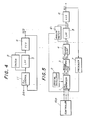
- the PLL synthesizer is made up of a PLL control circuit 11, a lowpass filter 5, a switch circuit 8 and a voltage-controlled oscillator (VCO) 6.
- the PLL control circuit 11 is supplied with set frequency data supplied from an external circuit, and an output signal derived from the VCO 6.
- the PLL control circuit 11 corresponds to the combination of the aforementioned PLL operation circuit 1, the crystal oscillator 2, the phase comparator 3 and the charge pump circuit 4.
- a signal supplied from the PLL control circuit 11 is supplied to the lowpass filter 5 and the switch circuit 8.
- the switch circuit 8 is maintained open, and the signal from the PLL control circuit 11 passes through only the lowpass filter 5, and is then supplied to the VCO 6.
- the switch circuit 8 is closed so that the input and output terminals of the lowpass filter 5 are short-circuited. Thereby, the signal derived from the PLL control circuit 11 is supplied directly to the VCO 6 through the switch circuit 8.
- the switch circuit 8 is made open so that the signal from the PLL control circuit 11 passes through only the lowpass filter 5.
- FIG.5 is a block diagram of a detailed configuration of the PLL synthesizer shown in FIG.4.
- the switch circuit 8 shown in FIG.4 is formed by an analog switch 81, which is controlled by the strobe signal STB supplied from a controller 100.
- the clock signal CK and set frequency data DA are also supplied from the controller 100.
- FIG.6 is a circuit diagram of the configuration shown in FIG.5.
- the charge pump circuit 4 includes a group of inverters 4a, a MOS (metal oxide semiconductor) transistor 4b, and two bipolar transistors 4c and 4d.
- the charge pump circuit 4 follows the phase comparator 3, which is followed by the PLL operation circuit 1.
- the PLL operation circuit 1 and the phase comparator 3 are formed using CMOS (complementary metal oxide semiconductor) techniques in a conventional manner.
- CMOS complementary metal oxide semiconductor
- the analog switch 81 is made up of two inverters 10a, 10b, and a bidirectional transfer gate 9 consisting of two MOS transistors.
- the strobe signal STB is supplied to the inverter 10a.
- the output signal of the inverter 10a is supplied to the inverter 10b and one of the two control terminals of the transfer gate 9.
- the other control terminal of the transfer gate 9 is supplied with the output signal of the inverter 10b.
- Two signal terminals of the transfer gate 9 are connected to the input and output terminals of the lowpass filter 5.
- the lowpass filter 5 consists of resistors and capacitors.
- the VCO 6 is a Colpitts oscillator, which includes capacitors C3, C4, C5 and a coil L2, and an oscillation transistor T1. Resistors R1 and R2 of the VCO 6 are used for defining a base potential, and a coil L1 is used for generating a collector potential. Capacitors C1 and C2 are used for separating an input terminal voltage VT from the aforementioned collector potential on the DC base.
- a voltage-controlled capacitor (Varicap) VC1 presents a variable capacitance based on the input terminal voltage VT. A variation in capacitance of the voltage-variable capacitor VC1 causes a change of the oscillation frequency of the Colpitts oscillator.
- a capacitor C6 is used for drawing the oscillation frequency through an AC coupling.
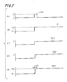
- the set frequency data DA is taken in the PLL operation circuit 1 when the strobe signal STB is supplied to the PLL operation circuit 1 as shown in (A) of FIG.7.
- the frequency of the set signal fr1 derived from the PLL operation circuit 1 is increased to the frequency fr2.
- the DC level of the signal SG1 is increased due to the function of the phase comparator 3 and the charge pump circuit 4.
- the analog switch 81 is closed by the strobe signal STB so that the output terminal of the charge pump circuit 4 is connected directly to the input terminal of the VCO 6.
- the signal SG1 is supplied directly to the VCO 6 through the analog switch 81, so that the signal SG2 increases rapidly as shown in (D) of FIG.7.
- the frequency of the output signal SG3 is rapidly increased from the frequency F1 to the frequency F2 with a slight lock-up time t2 as shown in (E) of FIG.7.
- the analog switch 81 is made open. Then the signal derived from the charge pump circuit 4 passes through the lowpass filter 5 and is supplied to the VCO 6.
- the output signal SG3 derived from the VCO 6 has a high purity, that is, less signal deterioration. It is preferable that the pulse width of the strobe signal STB is longer than the lock-up time.
- FIG.8 is a block diagram of a variation of the embodiment shown in FIG.5.
- the analog switch 81 of the variation shown in FIG.8 is supplied with a specific control signal CONT derived from the controller 100 separately from the strobe signal STB. That is, the analog switch 81 used in the variation is controlled by the specific control signal CONT, which rises in synchronism with the strobe signal, for example.
- FIG.9 is a block diagram of a second embodiment of the present invention.
- the illustrated PLL synthesizer has two lowpass filters 5 and 5a, which are connected in series.
- the analog switch 81 is connected across the lowpass filter 5. When the analog switch 81 is closed, the signal SG1 of the charge pump circuit 4 is supplied to the lowpass filter 5a through the analog switch 81. The signal SG1 passes through the lowpass filter 5a and is then supplied to the VCO 6.
- the arrangement shown in FIG.9 presents almost the same advantages as the arrangement shown in FIG.5.
- FIG.10A is a circuit diagram of the lowpass filters 5 and 5a.
- the lowpass filter 5 is formed by a resistor R11, and the lowpass filter 5a is composed of resistors R12, R13, and capacitors C11 and C12.
- An end of the resistor R11 is connected to the output terminal of the charge pump circuit 4.
- the output terminal of the analog switch 81 is connected to a connection node between the resistors R12 and R13.
- a connection node between the resistor R13 and the capacitor C12 is connected to the input terminal of the VCO 6.
- FIG.10B is a circuit diagram of a different configuration of the lowpass filters 5 and 5a.
- the lowpass filter 5 is formed by a resistor R21, and the lowpass filter 5a is composed of resistors R22 - R24, capacitors C22, C23 and a differential amplifier OP1.
- An end of the resistor R21 is connected to the output terminal of the charge pump circuit 4, and the other end thereof is connected to the inverting input terminal of the differential amplifier OP1.
- the non-inverting input terminal of the differential amplifier OP1 is supplied with a reference voltage Vref.
- the output terminal of the analog switch circuit 81 is connected to an end of the resistor R22, the other end of which is connected to the inverting input terminal of the differential amplifier OP1.
- a connection node between the resistor R24 and the capacitor C23 is connected to the input terminal of the VCO 6.
- the resistor R21 has a resistance of 8 k ⁇
- the resistor R22 has a resistance of 1 k ⁇ , for
- FIG.11A is a graph illustrating the experimental results obtained when the configuration shown in FIG.10A is used
- FIG.11b is a graph illustrating the experimental results obtained when the configuration shown in FIG.10B is used.
- the frequency of the VCO 6 was changed from 770 MHz to 814 MHz in response to the strobe signals shown in (A) of FIGS.11A and 11B.
- a curve CL1 shown in (B) of FIG.11A relates to a case where the analog switch 81 is held open independently of the strobe signal (A)
- a curve CL2 shown in (B) of FIG.11A relates to a case where the analog switch 81 is switched in synchronism with the strobe signal STB. It takes 150 ms the output frequency of the VCO 6 to be settled at 814 MHz in the absence of the analog switch control, whereas it takes 60 ms in the presence of the analog switch control according to the present invention.
- a curve CL3 shown in (B) of FIG.11B relates to a case where the analog switch 81 is held open independently of the strobe signal STB (A), and a curve CL4 shown in (B) of FIG.11B relates to a case where the analog switch 81 is switched in synchronism with the strobe signal STB. It takes 16 ms the output frequency of the VCO 6 to be settled at 814 MHz in the absence of the analog switch control, whereas it takes 8 ms in the presence of the analog switch control according to the present invention.
- the analog switch 81 shown in FIG.9 may be controlled by the specific control signal CONT separately from the strobe signal STB in the same way as the configuration shown in FIG.8.
- the switch circuit 8 is not limited to the analog switch 81. A mechanical switch or a digital switch may be used. It is preferably that the switch circuit 8 can operate at high speeds.
Landscapes
- Stabilization Of Oscillater, Synchronisation, Frequency Synthesizers (AREA)
Applications Claiming Priority (2)
| Application Number | Priority Date | Filing Date | Title |
|---|---|---|---|
| JP63332371A JPH02177725A (ja) | 1988-12-28 | 1988-12-28 | Pllシンセサイザ回路 |
| JP332371/88 | 1988-12-28 |
Publications (3)
| Publication Number | Publication Date |
|---|---|
| EP0376847A2 true EP0376847A2 (fr) | 1990-07-04 |
| EP0376847A3 EP0376847A3 (fr) | 1991-03-06 |
| EP0376847B1 EP0376847B1 (fr) | 1996-09-11 |
Family
ID=18254215
Family Applications (1)
| Application Number | Title | Priority Date | Filing Date |
|---|---|---|---|
| EP89403666A Expired - Lifetime EP0376847B1 (fr) | 1988-12-28 | 1989-12-27 | Synthétiseur à PLL |
Country Status (4)
| Country | Link |
|---|---|
| US (1) | US5047733A (fr) |
| EP (1) | EP0376847B1 (fr) |
| JP (1) | JPH02177725A (fr) |
| DE (1) | DE68927158T2 (fr) |
Cited By (6)
| Publication number | Priority date | Publication date | Assignee | Title |
|---|---|---|---|---|
| EP0476605A3 (en) * | 1990-09-19 | 1993-01-13 | Nec Corporation | Phase lock loop circuit comprising a subsidiary loop filter |
| EP0482823A3 (en) * | 1990-10-22 | 1993-06-09 | Nec Corporation | Pll frequency synthesizer capable of changing an output frequency at a high speed |
| FR2696299A1 (fr) * | 1992-09-25 | 1994-04-01 | Fujitsu Ltd | Circuit de synthétiseur de fréquence à boucle à verrouillage de phase. |
| WO1994021047A1 (fr) * | 1993-03-08 | 1994-09-15 | Nokia Telecommunications Oy | Procede de generation d'un signal d'horloge au moyen d'une boucle a verrouillage de phase, et boucle a verrouillage de phase utilisee |
| EP0782271A1 (fr) * | 1995-12-28 | 1997-07-02 | Thomson Consumer Electronics, Inc. | Boucle à verrouillage de phase à temps de réponse réglable |
| EP1341308A1 (fr) * | 2002-02-07 | 2003-09-03 | Nippon Telegraph and Telephone Corporation | Boucle à verrouillage de phase |
Families Citing this family (11)
| Publication number | Priority date | Publication date | Assignee | Title |
|---|---|---|---|---|
| JP2819876B2 (ja) * | 1991-08-20 | 1998-11-05 | 松下電器産業株式会社 | 周波数シンセサイザ |
| WO1993005578A1 (fr) * | 1991-08-30 | 1993-03-18 | Fujitsu Limited | Synthetiseur de frequence |
| FI98480C (fi) * | 1993-12-23 | 1997-06-25 | Nokia Mobile Phones Ltd | Menetelmä ja järjestely silmukkasuodattimen ohjaamiseksi |
| US5724008A (en) * | 1996-05-02 | 1998-03-03 | International Business Machines Corporation | Phase-locked loop with charge distribution |
| US5675292A (en) * | 1996-06-05 | 1997-10-07 | Mccune, Jr.; Earl W. | Phase lock loop enabling smooth loop bandwidth switching over a wide range |
| JP3024614B2 (ja) * | 1997-10-24 | 2000-03-21 | 日本電気株式会社 | ばらつき補償技術による半導体集積回路 |
| TW513860B (en) * | 2001-09-12 | 2002-12-11 | Via Tech Inc | Clock and data recovery circuit and related method |
| DE60314415T2 (de) * | 2003-08-29 | 2008-02-21 | Texas Instruments Inc., Dallas | Phasenregelschleife mit einer Ladungspumpe und Störunterdrückungsverbesserung der Stromversorgung |
| WO2005052820A1 (fr) * | 2003-10-31 | 2005-06-09 | International Business Machines Corporation | Procede et appareil permettant l'echelonnement d'une frequence au niveau d'un systeme dynamique |
| JP4598691B2 (ja) * | 2006-02-22 | 2010-12-15 | 富士通セミコンダクター株式会社 | Pll回路及び半導体装置 |
| JP2013090132A (ja) * | 2011-10-18 | 2013-05-13 | Renesas Mobile Corp | 半導体装置及びこれを搭載する無線通信端末 |
Family Cites Families (6)
| Publication number | Priority date | Publication date | Assignee | Title |
|---|---|---|---|---|
| JPS5533554B2 (fr) * | 1974-12-27 | 1980-09-01 | ||
| GB1529116A (en) * | 1976-06-25 | 1978-10-18 | Indesit | Receiver having a device for tuning the receiver to a selected signal frequency for reception by the receiver |
| US4330758A (en) * | 1980-02-20 | 1982-05-18 | Motorola, Inc. | Synchronized frequency synthesizer with high speed lock |
| US4516083A (en) * | 1982-05-14 | 1985-05-07 | Motorola, Inc. | Fast lock PLL having out of lock detector control of loop filter and divider |
| US4745372A (en) * | 1985-10-17 | 1988-05-17 | Matsushita Electric Industrial Co., Ltd. | Phase-locked-loop circuit having a charge pump |
| US4752749A (en) * | 1986-12-22 | 1988-06-21 | Rockwell International Corporation | Fast response tuner |
-
1988
- 1988-12-28 JP JP63332371A patent/JPH02177725A/ja active Pending
-
1989
- 1989-12-21 US US07/454,589 patent/US5047733A/en not_active Expired - Fee Related
- 1989-12-27 DE DE68927158T patent/DE68927158T2/de not_active Expired - Fee Related
- 1989-12-27 EP EP89403666A patent/EP0376847B1/fr not_active Expired - Lifetime
Cited By (14)
| Publication number | Priority date | Publication date | Assignee | Title |
|---|---|---|---|---|
| EP0476605A3 (en) * | 1990-09-19 | 1993-01-13 | Nec Corporation | Phase lock loop circuit comprising a subsidiary loop filter |
| EP0840457A3 (fr) * | 1990-10-22 | 1999-08-25 | NEC Corporation | Synthétiseur de fréquence à PLL permettant de changer la fréquence de sortie à une vitesse élevée |
| EP0482823A3 (en) * | 1990-10-22 | 1993-06-09 | Nec Corporation | Pll frequency synthesizer capable of changing an output frequency at a high speed |
| EP0840456A3 (fr) * | 1990-10-22 | 1999-08-25 | NEC Corporation | Synthétiseur de fréquence à PLL permettant de changer la fréquence de sortie à une vitesse élevée |
| FR2696299A1 (fr) * | 1992-09-25 | 1994-04-01 | Fujitsu Ltd | Circuit de synthétiseur de fréquence à boucle à verrouillage de phase. |
| US5410571A (en) * | 1992-09-25 | 1995-04-25 | Fujitsu Limited | PLL frequency synthesizer circuit |
| WO1994021047A1 (fr) * | 1993-03-08 | 1994-09-15 | Nokia Telecommunications Oy | Procede de generation d'un signal d'horloge au moyen d'une boucle a verrouillage de phase, et boucle a verrouillage de phase utilisee |
| GB2291548B (en) * | 1993-03-08 | 1997-01-08 | Nokia Telecommunications Oy | Method of generating a clock signal by means of a phase-locked loop and a phase-locked loop |
| GB2291548A (en) * | 1993-03-08 | 1996-01-24 | Nokia Telecommunications Oy | Method of generating a clock signal by means of a phase-locked loop and a phase-locked loop |
| EP0782271A1 (fr) * | 1995-12-28 | 1997-07-02 | Thomson Consumer Electronics, Inc. | Boucle à verrouillage de phase à temps de réponse réglable |
| US5748046A (en) * | 1995-12-28 | 1998-05-05 | Thomson Consumer Electronics, Inc. | Phase locked loop with controllable response time |
| CN1133271C (zh) * | 1995-12-28 | 2003-12-31 | 汤姆森消费电子有限公司 | 响应时间可控的锁相环 |
| EP1341308A1 (fr) * | 2002-02-07 | 2003-09-03 | Nippon Telegraph and Telephone Corporation | Boucle à verrouillage de phase |
| US6759912B2 (en) | 2002-02-07 | 2004-07-06 | Nippon Telegraph And Telephone Corporation | Phase locked loop |
Also Published As
| Publication number | Publication date |
|---|---|
| DE68927158D1 (de) | 1996-10-17 |
| DE68927158T2 (de) | 1997-02-06 |
| JPH02177725A (ja) | 1990-07-10 |
| US5047733A (en) | 1991-09-10 |
| EP0376847B1 (fr) | 1996-09-11 |
| EP0376847A3 (fr) | 1991-03-06 |
Similar Documents
| Publication | Publication Date | Title |
|---|---|---|
| US5047733A (en) | PLL synthesizer providing rapid frequency changeover | |
| US5389899A (en) | Frequency synthesizer having quick frequency pull in and phase lock-in | |
| US4752749A (en) | Fast response tuner | |
| JPH04223716A (ja) | Pllシンセサイザ回路 | |
| US5045818A (en) | PLL frequency modulator having bias voltage applied to filter capacitor | |
| JP2743133B2 (ja) | 位相検出器 | |
| US6949980B2 (en) | Phase-locked loop with high frequency adjustment of the operating range of the oscillator | |
| JPH1065525A (ja) | Pll回路 | |
| JPH06338793A (ja) | Pll周波数シンセサイザ回路 | |
| JPS5938761Y2 (ja) | Pll回路のロ−パスフィルタ | |
| JP2870466B2 (ja) | 位相同期回路 | |
| JPS5846586Y2 (ja) | 位相同期ル−プを有する回路 | |
| US5021752A (en) | Voltage controlled oscillator (VCO) | |
| JPS62290214A (ja) | 位相同期発振器 | |
| JPH02290332A (ja) | 位相ロックループ回路 | |
| JP2000004155A (ja) | Pll装置 | |
| JPH02154524A (ja) | シンセサイザ | |
| JPH03242017A (ja) | 高速・安定化電圧制御型発振回路 | |
| JP2976630B2 (ja) | 周波数シンセサイザ | |
| JPH08228148A (ja) | Pll制御方法 | |
| JPH03214925A (ja) | Pllシンセサイザ回路 | |
| JPS62176331A (ja) | フエ−ズロツクル−プ回路 | |
| JPS63126319A (ja) | 位相同期回路 | |
| JPH09238073A (ja) | 位相同期回路 | |
| JPH0653824A (ja) | 位相同期発振器 |
Legal Events
| Date | Code | Title | Description |
|---|---|---|---|
| PUAI | Public reference made under article 153(3) epc to a published international application that has entered the european phase |
Free format text: ORIGINAL CODE: 0009012 |
|
| AK | Designated contracting states |
Kind code of ref document: A2 Designated state(s): DE FR GB |
|
| PUAL | Search report despatched |
Free format text: ORIGINAL CODE: 0009013 |
|
| AK | Designated contracting states |
Kind code of ref document: A3 Designated state(s): DE FR GB |
|
| 17P | Request for examination filed |
Effective date: 19910810 |
|
| 17Q | First examination report despatched |
Effective date: 19931201 |
|
| GRAH | Despatch of communication of intention to grant a patent |
Free format text: ORIGINAL CODE: EPIDOS IGRA |
|
| GRAH | Despatch of communication of intention to grant a patent |
Free format text: ORIGINAL CODE: EPIDOS IGRA |
|
| GRAA | (expected) grant |
Free format text: ORIGINAL CODE: 0009210 |
|
| AK | Designated contracting states |
Kind code of ref document: B1 Designated state(s): DE FR GB |
|
| REF | Corresponds to: |
Ref document number: 68927158 Country of ref document: DE Date of ref document: 19961017 |
|
| ET | Fr: translation filed | ||
| PLBE | No opposition filed within time limit |
Free format text: ORIGINAL CODE: 0009261 |
|
| STAA | Information on the status of an ep patent application or granted ep patent |
Free format text: STATUS: NO OPPOSITION FILED WITHIN TIME LIMIT |
|
| PG25 | Lapsed in a contracting state [announced via postgrant information from national office to epo] |
Ref country code: FR Effective date: 19970829 |
|
| 26N | No opposition filed | ||
| REG | Reference to a national code |
Ref country code: FR Ref legal event code: ST |
|
| PGFP | Annual fee paid to national office [announced via postgrant information from national office to epo] |
Ref country code: GB Payment date: 19981231 Year of fee payment: 10 |
|
| PGFP | Annual fee paid to national office [announced via postgrant information from national office to epo] |
Ref country code: DE Payment date: 19990107 Year of fee payment: 10 |
|
| PG25 | Lapsed in a contracting state [announced via postgrant information from national office to epo] |
Ref country code: GB Free format text: LAPSE BECAUSE OF NON-PAYMENT OF DUE FEES Effective date: 19991227 |
|
| GBPC | Gb: european patent ceased through non-payment of renewal fee |
Effective date: 19991227 |
|
| PG25 | Lapsed in a contracting state [announced via postgrant information from national office to epo] |
Ref country code: DE Free format text: LAPSE BECAUSE OF NON-PAYMENT OF DUE FEES Effective date: 20001003 |