EP0379925A2 - Verfahren zur Herstellung einer dynamischen Speicherzelle mit wahlfreiem Zugriff - Google Patents
Verfahren zur Herstellung einer dynamischen Speicherzelle mit wahlfreiem Zugriff Download PDFInfo
- Publication number
- EP0379925A2 EP0379925A2 EP90100753A EP90100753A EP0379925A2 EP 0379925 A2 EP0379925 A2 EP 0379925A2 EP 90100753 A EP90100753 A EP 90100753A EP 90100753 A EP90100753 A EP 90100753A EP 0379925 A2 EP0379925 A2 EP 0379925A2
- Authority
- EP
- European Patent Office
- Prior art keywords
- film
- insulating film
- silicon oxide
- mask layer
- oxidizable
- Prior art date
- Legal status (The legal status is an assumption and is not a legal conclusion. Google has not performed a legal analysis and makes no representation as to the accuracy of the status listed.)
- Granted
Links
Images


Classifications
-
- H—ELECTRICITY
- H10—SEMICONDUCTOR DEVICES; ELECTRIC SOLID-STATE DEVICES NOT OTHERWISE PROVIDED FOR
- H10B—ELECTRONIC MEMORY DEVICES
- H10B12/00—Dynamic random access memory [DRAM] devices
- H10B12/01—Manufacture or treatment
-
- H—ELECTRICITY
- H10—SEMICONDUCTOR DEVICES; ELECTRIC SOLID-STATE DEVICES NOT OTHERWISE PROVIDED FOR
- H10D—INORGANIC ELECTRIC SEMICONDUCTOR DEVICES
- H10D1/00—Resistors, capacitors or inductors
- H10D1/01—Manufacture or treatment
- H10D1/045—Manufacture or treatment of capacitors having potential barriers, e.g. varactors
- H10D1/047—Manufacture or treatment of capacitors having potential barriers, e.g. varactors of conductor-insulator-semiconductor capacitors, e.g. trench capacitors
-
- H—ELECTRICITY
- H10—SEMICONDUCTOR DEVICES; ELECTRIC SOLID-STATE DEVICES NOT OTHERWISE PROVIDED FOR
- H10P—GENERIC PROCESSES OR APPARATUS FOR THE MANUFACTURE OR TREATMENT OF DEVICES COVERED BY CLASS H10
- H10P14/00—Formation of materials, e.g. in the shape of layers or pillars
- H10P14/60—Formation of materials, e.g. in the shape of layers or pillars of insulating materials
- H10P14/63—Formation of materials, e.g. in the shape of layers or pillars of insulating materials characterised by the formation processes
- H10P14/6302—Non-deposition formation processes
- H10P14/6304—Formation by oxidation, e.g. oxidation of the substrate
- H10P14/6306—Formation by oxidation, e.g. oxidation of the substrate of the semiconductor materials
- H10P14/6308—Formation by oxidation, e.g. oxidation of the substrate of the semiconductor materials of Group IV semiconductors
-
- H—ELECTRICITY
- H10—SEMICONDUCTOR DEVICES; ELECTRIC SOLID-STATE DEVICES NOT OTHERWISE PROVIDED FOR
- H10P—GENERIC PROCESSES OR APPARATUS FOR THE MANUFACTURE OR TREATMENT OF DEVICES COVERED BY CLASS H10
- H10P50/00—Etching of wafers, substrates or parts of devices
- H10P50/73—Etching of wafers, substrates or parts of devices using masks for insulating materials
Definitions
- This invention relates to a semiconductor memory device and, more particularly, to a process of fabricating a dynamic random access memory cell of one-transistor and one-capacitor type.
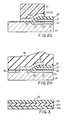
- FIG. 1A and 1B of the drawings A typical example of a process of fabricating a random access memory cell is shown in Figs. 1A and 1B of the drawings.
- the process starts with preparation of a p-type silicon substrate 1, and a thick field oxide film (not shown) is grown on the major surface of the silicon substrate 1 so that an active device area is defined by the thick field oxide film.
- a part of the silicon substrate 1 is heavily doped with n-type impurity atoms, and a lower electrode of a storage capacitor is formed in a part of the heavily doped n-type impurity region 11 thus produced, however, the end section (left side in Fig.
- the thin insulating film structure 2 is of a multi-film structure consisting of a lower thin silicon oxide film attached to the substrate 1, a silicon nitride film deposited on the lower thin silicon oxide film and an upper thin silicon oxide film formed on the silicon nitride film.
- a polysilicon which is etched and patterned for formation of an upper capacitor electrode 3 of the storage capacitor.
- the upper capacitor electrode 3 of the polysilicon is oxidized so that a silicon oxide is produced on the surface thereof.
- the silicon oxide film thus produced provides an inter-level insulating layer 4.
- the thin insulating film structure 2 is, then, partially removed until a fresh surface of the substrate 1 is exposed, and the thin insulating film structure 2 including the silicon nitride film and left beneath the capacitor electrode 3 serves as that dielectric film 2 of the storage capacitor (which is also formed in the multi-film structure of SiO2/Si3N4/SiO2).
- a gate silicon oxide film 5 of the switching transistor is thermally grown on the exposed surface of the silicon substrate 1, and a polysilicon film 6 is deposited over the entire surface as shown in Fig. 1A.
- the polysilicon film 6 is etched and patterned to form a gate electrode 7 of the switching transistor, and n-type impurity atoms are doped into the silicon substrate 1 by using the gate electrode 7 as a mask.
- the n-type impurity region 8 thus formed serves as the other of the source and drain regions of the switching transistor contiguous to a bit line, and an upper insulating oxide 9 is deposited on the entire surface of the structure as shown in Fig. 1B.
- the gate electrode 7 shown in Fig. 1B is partially overlapped with the capacitor electrode 3, however, the gate electrode may be spaced from the capacitor electrode without any overlapping in another implementation.
- a sharp step is inevitably formed at the side 12 of the inter-level insulating layer 4; more particularly, when the dielectric film 2 includes a silicon nitride film, an eaves-like shape 13 is formed at the foot of the side 12 of the insulating layer 4 because a lower portion of a side of the polysilicon electrode 7 attached to and near the dielectric film 2 is oxidized slower than other surface portions including an upper portion of the side of the electrode 7 during the oxidation process.
- the gate electrode 7 is partially overlapped with the capacitor electrode 3 as the structure shown in Fig. 1B, a problem is encountered in that the polysilicon film 6 is much liable to break at the foot of the inter-level insulating layer 4 encircled by a broken line 10 of Fig. 1B because of the sharp step and the eaves-like shape of the side of the inter-level insulating layer 4.
- the gate electrode 7 partially overlapped forms a parasitic capacitor together with the dielectric film 2 and the n+ type impurity region 11 consisting of the drain of the switching transistor and the lower electrode of the storage capacitor at the encircled portion 10, and the parasitic capacitance, that is, a gate-drain parasitic capacitance of the transistor is causative of decreasing the signal propagating speed of the transistor and introduces a large time delay in the switching action.
- the gate electrode within the eaves-like shape of the insulating layer 4 is further causative of reduction in withstand voltage level of the thin dielectric film 2.
- the gate electrode 7 is spaced from the capacitor electrode 3 in the lateral direction, a part of the gate electrode formed on and around the inter-level insulating layer 4 should be removed in the patterning stage of the polysilicon film 6. Then, a problem is encountered in that the other portion on the gate insulating film 5 is over-etched during the patterning stage of the gate electrode and the surface of the substrate is suffered damage. This is because of the fact that the polysilicon 7a at the step portion is much larger in thickness than the other such as being designated by 7b. Moreover, residual polysilicon tends to be left at the foot of the inter-level insulating layer 4 indicated by the circular broken line 10, and are causative of undesirable short circuit.
- the present invention proposes to previously and partially etching a surface portion of the inter-level structure in an anisotropical manner before patterning the capacitor electrode.
- a process of fabricating a random access memory cell having a storage capacitor and a switching transistor comprising the steps of: a) preparing an oxidizable semiconductor substrate having a capacitor forming portion; b) forming a dielectric film of the storage capacitor covering at least the capacitor forming portion and a transistor forming area of the oxidizable semiconductor substrate; c) forming a multiple-level structure having a first oxidizable conductive film on the dielectric film and a first insulating film on the first oxidizable conductive film, the multiple-level structure being provided on the entire structure; d) providing a first mask layer on the multiple-level structure and located over a capacitor electrode forming area; e) removing a surface portion of the first insulating film so that a hollow space extends beneath the first mask layer; f) removing the first insulating film and the first oxidizable conductive film by using the first mask layer, the hollow space causing a declining shoulder
- the process according to the present invention starts with a lightly doped p-type single crystal silicon substrate 21, and a thick field oxide film (not shown) is formed through a well-known selective oxidation process for defining an active device area.
- the silicon substrate 21 is selectively doped with n-type impurity atoms, so that a heavily doped impurity region 22 is formed in the silicon substrate 21.
- the heavily doped n-type impurity region 22 serves as a lower electrode of a storage capacitor at the major portion 22′ and as one of the source and drain regions of a switching transistor at the end portion 22 ⁇ .
- a dielectric film structure 23, a phosphorus doped polysilicon film 24 and a silicon oxide film 25 are successively stacked on the active device area of the silicon substrate 21.
- the dielectric film structure 23 is formed of a silicon nitride 23a sandwiched between silicon oxide films 23b and 23c (see Fig. 3), and the phosphorus doped polysilicon film 24 is deposited to a thickness of about 2000 angstroms to about 3000 angstroms by using, for example, a chemical vapor deposition technique.
- the silicon oxide film 25 is deposited by using another chemical vapor deposition technique, and the thickness thereof ranges from about 2000 angstroms to about 3000 angstroms.
- a photoresist solution is spun onto an entire surface of the structure for formation of a photoresist film, and the photoresist film is patterned through lithographic techniques, thereby being formed into a mask layer 26.
- the resultant structure of this stage is shown in Fig. 2A.
- the surface portion of the silicon oxide film 25 is isotropically etched away, and a bias takes place in the silicon oxide film 25 due to the equal etching rates between the vertical and lateral directions.
- the etching profile beneath the mask layer 26 appears as a generally quater-circle to form a hollow space 25′.
- a buffered fluoric acid is used as the isotropic etchant.
- the isotropic etching stage is followed by anisotropic dry etching stages, and the silicon oxide film 25 and, then, the phosphorus doped polysilicon film 24 are successively removed for defining an upper capacitor electrode 27.
- the left edge of the upper capacitor electrode 27 is aligned with the mask layer 26 as shown in Fig. 2B, and this configuration is conducive to forming a mild slope of an inter-level insulating layer.
- the mask layer 26 is stripped off, and the exposed portion of the dielectric film structure 23 is etched away.
- the silicon substrate 21 is placed in an oxidation ambient at about 900 degrees to about 950 degrees in centigrade for about 5 minutes to about 10 minutes, so that a silicon oxide film 28 is grown on the silicon substrate 21 and the silicon oxide film 25 is increased in thickness. Since the polysilicon doped with the phosphorus atoms promotes the oxidation, the silicon oxide film 25 is rapidly grown, but the silicon oxide film 28 is slowly grown so as to be relatively thin. The etching profile of the silicon oxide film 25 is upwardly transferred, and, for this reason, the left side of the upper portion thereof still appears as a generally quarter-circle. The resultant structure of this stage is shown in Fig. 2C.
- a silicon oxide film 29 is deposited by using the chemical vapor deposition technique, and is as thick as or greater than the total thickness of the silicon oxide film 25 and the capacitor electrode 27. In this instance, the silicon oxide film 29 ranges from about 4000 angstroms to about 6000 angstroms. The resultant structure of this stage is shown in Fig. 2D.
- the silicon oxide film 29 is uniformly removed in the vertical direction by using anisotropic etch-back technique, that is, a directional reactive ion etching for removing the film 29 predominately in the vertical direction until the fresh surface of the silicon substrate 21 is exposed. Since the silicon oxide film 25 has the left side of the upper portion shaped into the generally quarter-circle and the anisotropical etch-back is subjected to the film 29, the silicon oxide film covering the capacitor electrode 27 has a mild or non-steep shoulder portion 30a as shown in Fig. 2E, and serves as an inter-level insulating film 30. The exposed surface of the silicon substrate 21 is subjected to bombardment with the etchant and, for this reason, is liable to be damaged. However, if the exposed surface portion is slightly etched away by using a liquid etchant, a fresh surface without any damage is exposed again, and the contaminant is also removed from the silicon substrate 21.
- anisotropic etch-back technique that is,
- the silicon substrate 21 is placed in an oxidation ambient, and a thin gate oxide film 31 is thermally grown on the exposed surface of the silicon substrate 21. subsequently, a polysilicon film 32 is deposited on the entire surface of the structure. Since the inter-level insulating film 30 has the mild shoulder 30a, the polysilicon film 32 is generally uniform in thickness, and, for this reason, the thickness t1 on the bottom portion is nearly equal to the thickness t2 on the shoulder portion 30a. The resultant structure of this stage is shown in Fig. 2F.
- a photoresist solution is spun onto the entire structure, and the photoresist film is patterned to form a mask layer 33.
- the polysilicon film 32 is etched and patterned through the lithographic process, so that a gate electrode 34 is formed from the polysilicon film 32 as shown in Fig. 2G. Since the shoulder portion 30a of the inter-level insulating film 30 is mild in the decline, no disconnection takes place in the gate electrode 34. Moreover, the mild decline allows the inter-level insulating film 30 to be thick enough to decrease the parasitic capacitance produced thereacross. This results in improvement in switching speed.
- the photo-mask layer 33 is stripped off, and n-type impurity atoms are doped into the silicon substrate 21.
- the gate electrode 34 serves as the doping mask.
- the n-type impurity region 35 thus produced serves as the other of the source and drain regions of the switching transistor contiguous to a bit line, and the gate oxide film 31 and the gate electrode 34 as a whole constitute a gate structure of a switching transistor.
- the switching transistor selectively provides a channel between the source and drain regions 35 and 22 ⁇ , and a data bit in the form of electric charges is memorized into or read out from the storage capacitor.
- the storage capacitor has the n+ type lower capacitor electrode 22′, so that the storage capacitor can accumulate electric charges with a relatively low or the ground voltage level (which is approximately equal to the biasing voltage level of the substrate 21) applied to the capacitor electrode 27.
- no n+ type region may be formed as the lower capacitor electrode, and a positive voltage level may be applied to the capacitor electrode for formation of an inversion layer which serves as the lower capacitor electrode.
- FIG. 4A to 4I another process sequence is described, and the present invention is applied to a process of fabricating a trench type random access memory cell.
- the process starts with a single crystal silicon substrate 41 lightly doped with p-type impurity atoms, and a thick field oxide film 42 is, then, grown on the silicon substrate 41.
- An anisotropical etching technique such as, for example, a reactive ion etching technique is carried out for formation of a trench 43 defined by a wall portion.
- An n-type impurity atoms are doped into the wall portion, so that an n+ type impurity region 44 consisting of one of the source and drain regions 44 ⁇ of a switching transistor along the major surface portion of the substrate 41 and a lower electrode 44′ of a storage capacitor along the wall portion is formed.
- the resultant structure of this stage is shown in Fig. 4A.
- a thin oxide film is thermally grown on the entire surface, and a silicon nitride film and a silicon oxide film are successively deposited to form a triple level structure 45, so that the triple level structure 45 consists of the silicon nitride film sandwiched between the two silicon oxide films.
- This structure improves a resistivity against undesirable breaking down phenomenon at the corner edge of the trench.
- a doped polysilicon 46 is deposited on the entire surface, and the trench 43 is filled with the doped polysilicon 46.
- the doped polysilicon 46 further extends over the triple level structure 45.
- On the entire surface of the structure is deposited a silicon oxide film 47 onto which a photoresist solution is spun for forming a photo-resist film.
- the photo-resist film is patterned to provide a mask layer 48 which covers an upper capacitor electrode forming area.
- the resultant structure of this stage is shown in Fig. 4B.
- the silicon oxide film 47 is slightly etched away by using a buffered fluoric acid as an etchant, so that a hollow space 49 is formed in the surface portion of the silicon oxide film 47, and the hollow space 49 extends beneath the photo-mask 48 as shown in Fig. 4C.
- anisotropical etching stages are applied to the silicon oxide film 47 and the doped polysilicon 46, and the same mask layer 48 is used for the anisotropical etching stages.
- the silicon oxide film 47 thus patterned a generally quarter-circle hollow space is left, but the left side edge of a capacitor electrode 50 is substantially aligned with the left side edge of the mask layer 48 as shown in Fig. 4D.
- the exposed triple level structure 45 is partially removed from the upper surface of the silicon substrate 41, and the substrate is placed in an oxidizing ambient.
- a thin silicon oxide film 51 covers the exposed upper surface of the silicon substrate 41, and the silicon oxide film 47 is increased in the thickness due to the oxidation of the doped polysilicon 46.
- a silicon oxide film 52 is then deposited on the entire surface of the structure to a thickness equal to or greater than the total thickness of the silicon oxide film 47 and the doped polysilicon 46 as shown in Fig. 4E.
- An etch-back technique (which is described in the previous embodiment) is applied to the silicon oxide film 52 until the upper surface of the silicon substrate 41 is exposed. Since the silicon oxide film 47 has a mild shoulder portion at the left upper edge thereof, the silicon oxide film 52, which is merged with the silicon oxide film 47, smoothly extends toward the upper surface of the silicon substrate 41 as will be seen from Fig. 4F.
- the residual silicon oxide films 47 and 52 serves as an inter-level insulating film 53.
- a polysilicon film 54 is then deposited over the entire surface of the structure, and is smoothly declined by virtue of the smoothly declining surface of the inter-level insulating film 53 as shown in Fig. 4G.
- a photoresist solution is spun onto the entire surface, and is patterned through the lithographic techniques so that a mask layer 55 is formed on the polysilicon film 54.
- the polysilicon film 54 is patterned to form a gate electrode 56 of a switching transistor (see Fig. 4H), and, thereafter, the mask layer 55 is stripped off.
- n-type impurity atoms are selectively doped into a transistor forming area, and, for this reason, a source/drain region 57 contiguous to a bit line is formed in a self-align manner.
- an insulating film 58 is deposited over the entire surface of the structure, and the dynamic random access memory cell is completed as shown in Fig. 4I.
Landscapes
- Engineering & Computer Science (AREA)
- Manufacturing & Machinery (AREA)
- Semiconductor Memories (AREA)
Applications Claiming Priority (2)
| Application Number | Priority Date | Filing Date | Title |
|---|---|---|---|
| JP1013617A JP2503621B2 (ja) | 1989-01-23 | 1989-01-23 | 半導体装置の製造方法 |
| JP13617/89 | 1989-01-23 |
Publications (3)
| Publication Number | Publication Date |
|---|---|
| EP0379925A2 true EP0379925A2 (de) | 1990-08-01 |
| EP0379925A3 EP0379925A3 (de) | 1991-03-06 |
| EP0379925B1 EP0379925B1 (de) | 1995-04-26 |
Family
ID=11838191
Family Applications (1)
| Application Number | Title | Priority Date | Filing Date |
|---|---|---|---|
| EP90100753A Expired - Lifetime EP0379925B1 (de) | 1989-01-23 | 1990-01-15 | Verfahren zur Herstellung einer dynamischen Speicherzelle mit wahlfreiem Zugriff |
Country Status (4)
| Country | Link |
|---|---|
| US (1) | US4987091A (de) |
| EP (1) | EP0379925B1 (de) |
| JP (1) | JP2503621B2 (de) |
| DE (1) | DE69018839T2 (de) |
Cited By (1)
| Publication number | Priority date | Publication date | Assignee | Title |
|---|---|---|---|---|
| EP0848406A3 (de) * | 1996-12-13 | 1998-08-12 | Motorola, Inc. | Verfahren zur Herstellung einer Feldemissionsvorrichtung mit erniedrigtem Verlust zwischen Zeilen und Spalten |
Families Citing this family (4)
| Publication number | Priority date | Publication date | Assignee | Title |
|---|---|---|---|---|
| US5068707A (en) * | 1990-05-02 | 1991-11-26 | Nec Electronics Inc. | DRAM memory cell with tapered capacitor electrodes |
| JP2976585B2 (ja) * | 1991-05-10 | 1999-11-10 | ソニー株式会社 | 半導体装置の製造方法 |
| US5434098A (en) * | 1993-01-04 | 1995-07-18 | Vlsi Techology, Inc. | Double poly process with independently adjustable interpoly dielectric thickness |
| JP4961843B2 (ja) * | 2006-06-07 | 2012-06-27 | ソニー株式会社 | 記憶素子の製造方法 |
Family Cites Families (11)
| Publication number | Priority date | Publication date | Assignee | Title |
|---|---|---|---|---|
| US4164751A (en) * | 1976-11-10 | 1979-08-14 | Texas Instruments Incorporated | High capacity dynamic ram cell |
| US4112575A (en) * | 1976-12-20 | 1978-09-12 | Texas Instruments Incorporated | Fabrication methods for the high capacity ram cell |
| JPS5923476B2 (ja) * | 1978-07-13 | 1984-06-02 | 三菱電機株式会社 | 半導体装置の製造方法 |
| JPS5826829B2 (ja) * | 1979-08-30 | 1983-06-06 | 富士通株式会社 | ダイナミックメモリセルの製造方法 |
| JPS56137657A (en) * | 1980-03-29 | 1981-10-27 | Chiyou Lsi Gijutsu Kenkyu Kumiai | Manufacture of semiconductor device |
| US4409722A (en) * | 1980-08-29 | 1983-10-18 | International Business Machines Corporation | Borderless diffusion contact process and structure |
| JPS60245270A (ja) * | 1984-05-21 | 1985-12-05 | Hitachi Ltd | 半導体装置の製造方法 |
| JPS6230351A (ja) * | 1985-04-25 | 1987-02-09 | Nec Corp | 半導体装置の製造方法 |
| JPS63124533A (ja) * | 1986-11-14 | 1988-05-28 | Nec Corp | 半導体集積回路装置の製造方法 |
| JPS6427252A (en) * | 1987-04-13 | 1989-01-30 | Nec Corp | Semiconductor storage device |
| JPS63306652A (ja) * | 1987-06-08 | 1988-12-14 | Nec Corp | 半導体装置の製造方法 |
-
1989
- 1989-01-23 JP JP1013617A patent/JP2503621B2/ja not_active Expired - Lifetime
-
1990
- 1990-01-15 DE DE69018839T patent/DE69018839T2/de not_active Expired - Fee Related
- 1990-01-15 EP EP90100753A patent/EP0379925B1/de not_active Expired - Lifetime
- 1990-01-22 US US07/468,212 patent/US4987091A/en not_active Expired - Fee Related
Cited By (1)
| Publication number | Priority date | Publication date | Assignee | Title |
|---|---|---|---|---|
| EP0848406A3 (de) * | 1996-12-13 | 1998-08-12 | Motorola, Inc. | Verfahren zur Herstellung einer Feldemissionsvorrichtung mit erniedrigtem Verlust zwischen Zeilen und Spalten |
Also Published As
| Publication number | Publication date |
|---|---|
| EP0379925A3 (de) | 1991-03-06 |
| US4987091A (en) | 1991-01-22 |
| DE69018839T2 (de) | 1995-10-12 |
| JPH02194554A (ja) | 1990-08-01 |
| EP0379925B1 (de) | 1995-04-26 |
| JP2503621B2 (ja) | 1996-06-05 |
| DE69018839D1 (de) | 1995-06-01 |
Similar Documents
| Publication | Publication Date | Title |
|---|---|---|
| US5976945A (en) | Method for fabricating a DRAM cell structure on an SOI wafer incorporating a two dimensional trench capacitor | |
| US6399978B2 (en) | Formation of 5F2 cell with partially vertical transistor and gate conductor aligned buried strap with raised shallow trench isolation region | |
| US6049093A (en) | Planar thin film transistor formation | |
| JP3229665B2 (ja) | Mosfetの製造方法 | |
| US5880496A (en) | Semiconductor having self-aligned polysilicon electrode layer | |
| US5482869A (en) | Gettering of unwanted metal impurity introduced into semiconductor substrate during trench formation | |
| JP3146316B2 (ja) | 半導体装置及びその製造方法 | |
| US6569729B1 (en) | Method of fabricating three dimensional CMOSFET devices for an embedded DRAM application | |
| KR940006681B1 (ko) | 스택트렌치 셀 및 그 제조방법 | |
| US5591670A (en) | Method of manufacturing a semiconductor device having self aligned contact hole | |
| US5710075A (en) | Method to increase surface area of a storage node electrode, of an STC structure, for DRAM devices | |
| US5372965A (en) | Method for fabricating capacitor of semiconductor memory device | |
| US4987091A (en) | Process of fabricating dynamic random access memory cell | |
| JP2796249B2 (ja) | 半導体記憶装置の製造方法 | |
| US5792688A (en) | Method to increase the surface area of a storage node electrode, of an STC structure, for DRAM devices, via formation of polysilicon columns | |
| US5567639A (en) | Method of forming a stack capacitor of fin structure for DRAM cell | |
| KR940010346A (ko) | 반도체 집적 소자의 디램(dram) 제조방법 | |
| JPH08181327A (ja) | 薄膜トランジスタ及びその製造方法 | |
| KR100227958B1 (ko) | 반도체 장치 및 제조방법 | |
| US6080622A (en) | Method for fabricating a DRAM cell capacitor including forming a conductive storage node by depositing and etching an insulative layer, filling with conductive material, and removing the insulative layer | |
| JP3190144B2 (ja) | 半導体集積回路の製造方法 | |
| JP3085831B2 (ja) | 半導体装置の製造方法 | |
| JP3204872B2 (ja) | Mosfet及びその製造方法 | |
| JP3063203B2 (ja) | 半導体メモリ及びその製造方法 | |
| KR100190524B1 (ko) | 반도체 소자의 전하 저장전극의 제조방법 |
Legal Events
| Date | Code | Title | Description |
|---|---|---|---|
| PUAI | Public reference made under article 153(3) epc to a published international application that has entered the european phase |
Free format text: ORIGINAL CODE: 0009012 |
|
| 17P | Request for examination filed |
Effective date: 19900329 |
|
| AK | Designated contracting states |
Kind code of ref document: A2 Designated state(s): DE FR GB |
|
| PUAL | Search report despatched |
Free format text: ORIGINAL CODE: 0009013 |
|
| RHK1 | Main classification (correction) |
Ipc: H01L 21/82 |
|
| AK | Designated contracting states |
Kind code of ref document: A3 Designated state(s): DE FR GB |
|
| 17Q | First examination report despatched |
Effective date: 19931011 |
|
| GRAA | (expected) grant |
Free format text: ORIGINAL CODE: 0009210 |
|
| AK | Designated contracting states |
Kind code of ref document: B1 Designated state(s): DE FR GB |
|
| REF | Corresponds to: |
Ref document number: 69018839 Country of ref document: DE Date of ref document: 19950601 |
|
| ET | Fr: translation filed | ||
| PLBE | No opposition filed within time limit |
Free format text: ORIGINAL CODE: 0009261 |
|
| STAA | Information on the status of an ep patent application or granted ep patent |
Free format text: STATUS: NO OPPOSITION FILED WITHIN TIME LIMIT |
|
| 26N | No opposition filed | ||
| PGFP | Annual fee paid to national office [announced via postgrant information from national office to epo] |
Ref country code: DE Payment date: 20010108 Year of fee payment: 12 |
|
| PGFP | Annual fee paid to national office [announced via postgrant information from national office to epo] |
Ref country code: GB Payment date: 20010110 Year of fee payment: 12 |
|
| PGFP | Annual fee paid to national office [announced via postgrant information from national office to epo] |
Ref country code: FR Payment date: 20010125 Year of fee payment: 12 |
|
| REG | Reference to a national code |
Ref country code: GB Ref legal event code: IF02 |
|
| PG25 | Lapsed in a contracting state [announced via postgrant information from national office to epo] |
Ref country code: GB Free format text: LAPSE BECAUSE OF NON-PAYMENT OF DUE FEES Effective date: 20020115 |
|
| PG25 | Lapsed in a contracting state [announced via postgrant information from national office to epo] |
Ref country code: DE Free format text: LAPSE BECAUSE OF NON-PAYMENT OF DUE FEES Effective date: 20020801 |
|
| GBPC | Gb: european patent ceased through non-payment of renewal fee |
Effective date: 20020115 |
|
| PG25 | Lapsed in a contracting state [announced via postgrant information from national office to epo] |
Ref country code: FR Free format text: LAPSE BECAUSE OF NON-PAYMENT OF DUE FEES Effective date: 20020930 |
|
| REG | Reference to a national code |
Ref country code: FR Ref legal event code: ST |