EP0399362B1 - Un circuit amplificateur de lecture - Google Patents
Un circuit amplificateur de lecture Download PDFInfo
- Publication number
- EP0399362B1 EP0399362B1 EP90109264A EP90109264A EP0399362B1 EP 0399362 B1 EP0399362 B1 EP 0399362B1 EP 90109264 A EP90109264 A EP 90109264A EP 90109264 A EP90109264 A EP 90109264A EP 0399362 B1 EP0399362 B1 EP 0399362B1
- Authority
- EP
- European Patent Office
- Prior art keywords
- bit line
- excess charge
- transistor
- sense amplifier
- voltage
- Prior art date
- Legal status (The legal status is an assumption and is not a legal conclusion. Google has not performed a legal analysis and makes no representation as to the accuracy of the status listed.)
- Expired - Lifetime
Links
Images


Classifications
-
- G—PHYSICS
- G11—INFORMATION STORAGE
- G11C—STATIC STORES
- G11C16/00—Erasable programmable read-only memories
- G11C16/02—Erasable programmable read-only memories electrically programmable
- G11C16/06—Auxiliary circuits, e.g. for writing into memory
-
- G—PHYSICS
- G11—INFORMATION STORAGE
- G11C—STATIC STORES
- G11C7/00—Arrangements for writing information into, or reading information out from, a digital store
- G11C7/06—Sense amplifiers; Associated circuits, e.g. timing or triggering circuits
- G11C7/067—Single-ended amplifiers
-
- G—PHYSICS
- G11—INFORMATION STORAGE
- G11C—STATIC STORES
- G11C16/00—Erasable programmable read-only memories
- G11C16/02—Erasable programmable read-only memories electrically programmable
- G11C16/06—Auxiliary circuits, e.g. for writing into memory
- G11C16/26—Sensing or reading circuits; Data output circuits
-
- G—PHYSICS
- G11—INFORMATION STORAGE
- G11C—STATIC STORES
- G11C17/00—Read-only memories programmable only once; Semi-permanent stores, e.g. manually-replaceable information cards
- G11C17/08—Read-only memories programmable only once; Semi-permanent stores, e.g. manually-replaceable information cards using semiconductor devices, e.g. bipolar elements
- G11C17/10—Read-only memories programmable only once; Semi-permanent stores, e.g. manually-replaceable information cards using semiconductor devices, e.g. bipolar elements in which contents are determined during manufacturing by a predetermined arrangement of coupling elements, e.g. mask-programmable ROM
- G11C17/12—Read-only memories programmable only once; Semi-permanent stores, e.g. manually-replaceable information cards using semiconductor devices, e.g. bipolar elements in which contents are determined during manufacturing by a predetermined arrangement of coupling elements, e.g. mask-programmable ROM using field-effect devices
-
- G—PHYSICS
- G11—INFORMATION STORAGE
- G11C—STATIC STORES
- G11C7/00—Arrangements for writing information into, or reading information out from, a digital store
- G11C7/12—Bit line control circuits, e.g. drivers, boosters, pull-up circuits, pull-down circuits, precharging circuits, equalising circuits, for bit lines
Definitions
- the present invention relates to a sense amplifier circuit for a reading circuit of a semiconductor memory apparatus, and more particularly to a sense amplifier circuit for a read only memory.
- Recent non-volatile memories such as read-only memories (called ROM hereinafter) are required to have large capacity and to operate at high speed.
- ROM read-only memories
- the memory cell area must be decreased, even if this requires that the current-driving ability of the memory cell transistor be decreased.
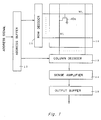
- a ROM is formed as shown in Figure 1.
- 10 is a memory cell array comprising a plurality of word lines WL and bit lines BL, and a memory cell 10a provided at respective crossing portions of these word lines WL and bit lines BL.
- Memory cell 10a comprises, for example, a MOS transistor whose gate is connected to word line WL and whose drain is connected to bit line BL.
- Memory cell 10a may comprise a bipolar transistor.
- Word lines WL are selected by row decoder 11 and bit lines BL are selected by column decoder 12, and an address signal is input to these row and column decoders through address buffer 13.
- the read output of a bit line BL selected by the column decoder 12 is amplified by sense amplifier 14 and is outputted externally through output buffer 15.
- Fig. 2 shows the general constitution of a known sense amplifier circuit.
- a sense amplifier circuit comprises a serial connection of a load 21, a transistor 21 and a memory cell 20, being connected between a power source V CC and ground GND.
- Memory cell 20 comprises a plurality of memory cells 20a, 20b.... as shown in Figures 3A and 3B.
- Figure 3A designates a serial type memory cell
- Figure 3B designates a parallel type memory cell.
- memory cells 20a, 20b... which are formed of transistors, store either "1 " or "0” depending on whether the transistor is of an enhancement type or of a depletion type.
- "1" or "0" is stored depending on whether the threshold value is high or low.
- the non-selection word line is made to level H and the selection word line is made to level L.
- the word line WLb is selected, other word lines WLa, WLc, ... are at H level and transistors 20a, 20c... are on regardless of whether the stored value is "1" or "0". Only transistor 20b, belonging to the selected word line, is turned on and off, depending on whether 1 or 0 is stored. If transistor 20b is of the depletion type it is on and if it is of the enhancement type it is off.
- the data stored in memory cell 20b is determined to be 1 or 0, and thus a current flows or does not flow in bit line BLa.
- the potential V C at the connecting point between load 21 and transistor Q1 in Figure 2 changes depending on whether or not the bit line current (i cel ) flows and voltage output circuit 22 detects potential V C and produces read out data.
- the selected word line is at H level and the non-selected word line is at L level. Accordingly, memory cells belonging to non-selected word lines are turned off regardless of whether "1" or “0” is stored, and only the memory cell belonging to the selected word line is turned on or off depending on whether “1” or “0” is stored. A current flows or does not flow in bit line BLa, depending on whether the memory cell is turned on or off, thereby changing the voltage V C . Voltage output circuit 22 then detects the voltage V C and produces the read-out data. Voltage output circuit 22 basically comprises only a line, but may be formed of a circuit for driving an output side circuit to be connected to the sense amplifier.
- a column selection gate which is turned on or off depending on the output of decoder 12, is provided between transistor Q1 and the bit line (cell group).
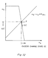
- the variation of the bit line voltage v a is suppressed, whether the bit line current I CEL is turned on or off.
- the voltage V C is equal to VCC-Rx icel under the condition that the resistance of load 21 is R and changes as shown in the drawing, depending on whether the cell is switched on or off.
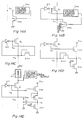
- Figures 4A to 4H Various kinds of inverters 23 are shown in Figures 4A to 4H.
- Figure 4A shows an E-D type
- Figure 4B an E-E type
- Figure 4C and Figure 4D CMOS types in which Qa is an n-channel enhancement type MOS transistor, Qb is an n-channel depletion type MOS transistor and Qd is a p-channel type MOS transistor.
- Figures 4E to 4H show only load portions.
- the gate of p-channel type transistor Qd is connected to ground in Figures 4C and 4G, connected to input IN in Figure 4D and connected to the drain (output OUT) in Figure 4H.
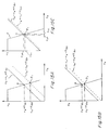
- the input-output characteristic of inverter 23 is shown in Figure 6.
- the current is divided into several steps and for binary-value logic, the two states, i.e., the state in which current flows and the state in which current does not flow, are provided. Let us explain the example of two steps in which the current flows or does not flow.
- the output of inverter 23 is fed back to the input of inverter 23 through transistor Q1.
- the input-output characteristic of the inverter is abrupt. Therefore, the range of variation of v a can be made small, and v b can be changed quickly. That is, the variation of V a is made small so that the existence of a bit line capacitance shown in Figure 7 does not greatly affect the operation of the cell 20, and the range of the variation in v b is made large, thus enabling the on/off control of transistor Q1 to be conducted at high speed and with certainty.
- a column selection gate shown in Figure 7 is connected between a cell 20 and a sense amplifier comprising transistor Q1, inverter 23 and load 21 and has a relatively large capacitance.
- a parasitic capacitance C WB exists between bit line BL and word line WL.
- C BL is a parasitic capacitance existing between bit line BL and ground.
- the bit line potential is almost equal to v a .
- a change in v a means that the bit line potential changes and that the charges stored in bit line capacitances C BL and C WB change accordingly.
- the sense amplifier operates only after the excess charge is discharged by the cell transistor.
- the reason for the above operation is that a variation in word line potential is reflected on a bit line by a parasitic capacitance C WB between a word line and a bit line and that an operation point of a sense amplifier varies in accordance with a power source potential variation caused by a noise.
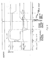
- v a increases and v b decreases, thereby providing a new stable state under the voltage V CC + ⁇ V (state C, b ⁇ c).
- V CC voltage + ⁇ V
- a time delay or a surplus time period shown in a state F′ and d ⁇ a time delay is relatively unimportant, but when the current driving capability of the cell, i.e., the current driving capability by which the input-output characteristic is driven from d to e, becomes weak because of a fine pattern of the cell, the time delay in this surplus time period F′ becomes large, greatly affecting access time.
- An object of the present invention is to make improvements regarding the above points and, by preventing excess charge-up of bit line capacitance, to realize a sense amplifier with high speed operation.
- a feature of the present invention resides in a sense amplifier circuit for use in a non-volatile memory comprising, an excess charge detecting circuit for producing a detection output when the potential of a bit line exceeds a normal value, an excess charge discharging circuit which operates in response to said excess charge detecting circuit for discharging a bit line charge and for returning the bit line potential to the normal value.
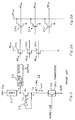
- the present invention provides a circuit 24 for detecting an excess charge up of a bit line and an excess charge discharging circuit 25 to be operated by the output of detecting circuit 24.
- excess charge up can be detected as an increase in potential.
- excess charge detecting circuit 24 receives a bit line potential v a and detects the excess charge up.
- excess charge detecting circuit 24 receives the output voltage v b (a gate voltage of transistor Q1) from inverter 23 and, as shown in Figure 11D, receives both voltages v a and v b .
- excess charge discharging circuit 25 operates to discharge the excess bit line charge.
- bit line potential decreases, deviating from the excess charge up state, and discharging circuit 25 stops the operation.
- the excess charge detecting circuit of Figures 11A, 11B and 11C detects an abnormality of v a , v b , and v b - v a .
- excess charge detecting circuit 24 comprises voltage judging circuit 24a for judging the voltage v a and excess charge discharging circuit 25 comprises a transistor 25a connected between the bit line and ground.
- An inverter shown in Figure 4A to 4H or comparator CMP shown in Figure 13C can be used for voltage judging circuit 24a.
- the inverter detects an excess charge based on whether or not the voltage v a exceeds a threshold value and the comparator detects the excess charge based on whether or not the voltage v a exceeds a reference voltage REF.
- the output of voltage judging circuit 24a becomes H level and transistor 25a is turned ON, thereby discharging the bit line charge.
- the output of voltage judging circuit 24a becomes L and transistor 25a is turned OFF, thereby stopping the discharge.
- voltage judging circuit 24a observes the output of the inverter and transistor 25a turns ON when the inverter output v b decreases and becomes less than the threshold value or the reference voltage.
- Figures 14A and 14B are similar to Figures 13A and 13B.
- n-channel transistor 25a is used but in Figures 14A and 14B, p-channel transistor 25b is used. Except for this feature, Figures 14A and 14B are the same as Figures 13A and 13B.
- excess charge detecting circuit 24 and excess charge discharging circuit 25 are formed of a single transistor 25c.
- This transistor 25c is diode-connected and the threshold value is determined as V th2 .
- transistor 25c turns ON, thereby discharging the charge.
- This state is shown in Figure 15A. Although the correction is lacking by P1 - P as compared with a normal state, the circuit is made simple.
- excess charge detecting circuit 24 and excess charge discharging circuit 25 are formed of n-channel transistor 24b, 24c and 25d.
- the voltage at the serial connecting point between transistors 24b and 24c is determined as V d .
- transistor 25d turns ON and transistor 25c is normally ON, thereby discharging the excess bit-line charge.
- V d is smaller than v b by the threshold value V th3 of transistor 24b and thus, point P1 is made closer to point P than in Figure 14C.
- excess charge detecting circuit 24 is formed of n-channel MOS transistors 24b, 24d and 24c and excess charge discharging circuit 25 is formed of p-channel transistor 25b.
- transistor 25b when transistor 25b is determined to have threshold value v th2 , and then v a - v d ⁇ V th2 , transistor 25b turns ON, thereby discharging the bit-line excess charge.
- v a1 - v a0 (V thN - V thp )/(1 + A)
- v b0 - v b1 A(V thN - V thp )/(1 + A) ⁇ V thN - V thp
- VthN ⁇ Vthp (generally speaking, the difference is about 100mV), Va1 ⁇ Vao and Vpo ⁇ Vp1.
- the present invention can prevent the bit line potential from being charged up to more than the predetermined value and can decrease the sense time delay caused by an excess charge-discharge and further can sense the data at high speed even for a cell with a weak current driving capability, thereby contributing to the high density of the integration.
Landscapes
- Read Only Memory (AREA)
- Semiconductor Memories (AREA)
Claims (17)
- Circuit d'amplification de détection, connecté à une ligne de bit, dans une mémoire non volatile, comprenant :
un moyen de détection de charge en excès (24) permettant de produire une sortie de détection lorsqu'un potentiel d'une ligne de bit dépasse une valeur prédéterminée, et
un moyen de décharge de charge en excès (25) permettant de décharger une charge de ligne de bit afin de remettre le potentiel de ligne de bit à la valeur prédéterminée en réponse à ladite sortie de détection (figure 11A). - Circuit d'amplification de détection selon la revendication 1, dans lequel ledit moyen de détection de charge en excès (24) comprend un inverseur (24a) pour détecter la charge en excès sur la base d'une tension de seuil de l'inverseur.
- Circuit d'amplification de détection selon la revendication 1, dans lequel ledit moyen de détection de charge en excès (24) comprend un comparateur (CMP) pour détecter la charge en excès sur la base d'une tension de référence appliquée au comparateur.
- Dispositif de mémoire non volatile comprenant un circuit d'amplification de détection selon la revendication 1, comprenant en outre :
une pluralité de lignes de bit (BL) ;
une pluralité de cellules de mémoire (10a) connectées auxdites lignes de bit ;
ledit circuit d'amplification de détection comprenant :
un moyen d'amplification (21, Q1, 23) permettant de détecter des données provenant de ladite ligne de bit ; et
une porte de colonne (12) connectée entre ledit moyen d'amplification (21, Q1, 23) et lesdites lignes de bit (BL). - Dispositif de mémoire non volatile selon la revendication 4, dans lequel ledit moyen de détection de charge en excès comprend un circuit d'évaluation de tension (24a) connecté à une borne d'entrée dudit moyen d'amplification (14), produisant une sortie de détection lorsque le potentiel d'entrée dépasse ledit potentiel prédéterminé, ledit moyen de décharge de charge en excès comprenant un transistor de décharge (25b), connecté à ladite borne d'entrée dudit moyen d'amplification (14), déchargeant la charge en excès en réponse à la sortie de détection (figure 14A).
- Circuit d'amplification de détection selon la revendication 1, dans lequel ladite mémoire non volatile comprend une pluralité de cellules de mémoire (10a) connectées aux lignes de bit (BL) ; et ledit circuit d'amplification de détection comprend en outre :
un moyen d'amplification comprenant une charge (21), un transistor (Q1) connecté entre ladite charge (21) et chacune desdites lignes de bit (BL) et un inverseur (23) connecté entre chacune desdites lignes de bit (BL) et une grille dudit transistor (Q1), afin de détecter les données provenant de ladite ligne de bit (BL) ;
ledit moyen de détection de charge en excès (24) détectant une charge en excès dans ledit moyen d'amplification afin de décharger la charge en excès et ledit moyen de détection de charge en excès étant sensible à la sortie dudit inverseur (23) (figure 11C). - Circuit d'amplification de détection selon la revendication 1, dans lequel ledit moyen de détection de charge en excès comprend un circuit d'évaluation de tension (24a) connecté à la ligne de bit (BL) et ledit moyen de décharge de charge en excès comprend un transistor (25b) dont le drain est connecté à la ligne de bit (BL) et dont la grille est connectée à la sortie dudit circuit d'évaluation de tension (24a) (figure 14A).
- Circuit d'amplification de détection selon la revendication 1, dans lequel ladite mémoire non volatile comprend une pluralité de cellules de mémoire (10a) connectées aux lignes de bit (BL) ; et ledit circuit d'amplification de détection comprend en outre :
un moyen d'amplification comprenant une charge (21), un transistor (Q1) connecté entre ladite charge (21) et chacune desdites lignes de bit (BL) et un inverseur (23) connecté entre chacune desdites lignes de bit (BL) et une grille dudit transistor (Q1), afin de détecter les données provenant de ladite ligne de bit (BL) ;
ledit moyen de détection de charge en excès (24) détectant une charge en excès dudit moyen d'amplification afin de décharger la charge en excès et ledit moyen de détection de charge en excès étant sensible au potentiel de ladite ligne de bit (BL) et à la sortie dudit inverseur (23) (figure 11B). - Circuit d'amplification de détection selon la revendication 8, dans lequel ledit moyen de décharge de charge en excès comprend un transistor connecté à une diode (25c) dont la première borne est connectée à la ligne de bit (BL) et dont la seconde borne est connectée à la sortie de l'inverseur (23), ledit transistor connecté à une diode (25c) étant rendu passant lorsque la tension de ligne de bit dépasse la tension prédéterminée, diminuant ainsi la tension de ligne de bit (figure 14C).
- Circuit d'amplification de détection selon la revendication 8, dans lequel ledit moyen de détection de charge en excès comprend :
un premier transistor (24b), dont la grille est connectée à la sortie de l'inverseur (23) et dont la première borne est connectée à une source de tension, pour diminuer la sortie dudit inverseur (23) de la première tension de seuil du premier transistor (24b),
ledit moyen de décharge de charge en excès comprenant :
un transistor monté en diode (25d) dont la première borne est connectée à la ligne de bit (BL) afin d'augmenter la sortie dudit premier transistor (24b) de la seconde tension de seuil, ledit transistor monté en diode (25d) étant rendu passant lorsque la tension de ligne de bit dépasse la tension prédéterminée ; et
un second transistor (24c) dont la première borne est connectée à la seconde borne dudit premier transistor (24b) et dont la seconde borne est connectée à la masse, la seconde borne du transistor monté en diode (25d) étant connectée à la fois à la seconde borne du premier transistor (24b) et à la première borne du second transistor (24c), et ledit second transistor (24c) déchargeant la charge en excès (Figure 14D). - Circuit d'amplification de détection selon la revendication 6, dans lequel ledit moyen de détection de charge en excès comprend :
un premier transistor à canal n (24b) présentant une première borne connectée à une source de tension et présentant une grille connectée à la sortie dudit inverseur (23) pour diminuer la sortie dudit inverseur (23) ;
un second transistor à canal n (24d) présentant un mode de montage en diode et possédant une première borne connectée à la seconde borne dudit premier transistor à canal n pour diminuer la tension de sortie dudit premier transistor à canal n de sa tension de seuil ; et
ledit moyen de décharge de charge en excès comprenant :
un transistor à canal p (25b) présentant une première borne connectée à ladite ligne de bit (BL) et présentant une seconde borne connectée à la terre pour augmenter la tension de ligne de bit de sa tension de seuil et pour augmenter la sortie dudit second transistor à canal n de sa tension de seuil,
dans lequel la charge en excès de ligne de bit se décharge au travers dudit transistor à canal p (25b) lorsque la charge d'excès de ligne de bit dépasse la valeur prédéterminée (figure 14E). - Circuit d'amplification de détection selon la revendication 1, dans lequel ledit moyen de décharge de charge en excès comprend des transistors MOS à canal n ou à canal p (25b) connectés entre ladite ligne de bit (BL) et la terre.
- Circuit d'amplification de détection selon la revendication 1, dans lequel ladite mémoire non volatile comprend une cellule connectée à une ligne de bit (BL) et une ligne de mot (WL) ; ledit circuit d'amplification de détection comprenant en outre :
un moyen de détection (23, Q1) permettant de détecter un courant circulant dans la ligne de bit (BL) en réponse à un état de fonctionnement de la cellule. - Circuit d'amplification de détection selon la revendication 13, dans lequel ledit moyen de décharge de charge en excès comprend un moyen (25a) déterminant la circulation d'un courant depuis la ligne de bit (BL) jusqu'au dit moyen de détection (23, Q1) lorsque la tension de ligne de bit dépasse une valeur prédéterminée.
- Circuit d'amplification de détection selon la revendication 13, dans lequel ledit moyen de détection de charge en excès comprend :
un moyen (24b) permettant de diminuer une tension obtenue à partir dudit moyen de détection (23, Q₁) d'une première valeur prédéterminée ;
ledit moyen de décharge de charge en excès comprenant :
un moyen (25d) permettant d'augmenter la sortie dudit moyen de diminution d'une seconde valeur prédéterminée ;
un moyen (24c) permettant de décharger un courant lorsque la tension de ligne de bit dépasse une valeur prédéterminée (figure 14D). - Circuit d'amplification de détection selon la revendication 13, dans lequel ledit moyen de détection de charge en excès comprend :
un premier moyen (24b) d'un type de conductivité permettant de diminuer une tension obtenue à partir dudit moyen de détection (23, Q1) d'une première valeur prédéterminée ;
un second moyen (24d) d'un type de conductivité permettant de diminuer la valeur de sortie dudit premier moyen d'une seconde valeur prédéterminée ; et
ledit moyen de décharge de charge en excès comprenant un troisième moyen (25b) de l'autre type de conductivité permettant d'augmenter la sortie dudit second moyen d'une troisième valeur prédéterminée (figure 14E). - Circuit d'amplification de détection selon la revendication 1, dans lequel ladite mémoire non volatile comprend un cellule connectée à une ligne de bit (BL) et à une ligne de mot (WL) ; ledit circuit d'amplification de détection comprenant en outre :
un moyen de charge (21) présentant une borne connectée à une source de tension ;
un moyen de transistor de détection (Q1) présentant une borne connectée à l'autre borne de ladite charge (21) et présentant l'autre borne connectée à la ligne de bit (BL) pour détecter un courant circulant au travers de ladite cellule ;
un moyen d'inversion (23) connecté à ladite ligne de bit (BL) permettant d'inverser une tension de ligne de bit afin d'appliquer une tension inversée à une grille dudit moyen de transistor de détection (Q1) ; et
ledit moyen de décharge de charge en excès comprend un moyen de transistor monté en diode (25c) possédant son drain connecté à la ligne de bit (BL) afin d'empêcher la tension de ligne de bit de dépasser une valeur prédéterminée en étant rendu passant lorsque la tension de bit est voisine d'une valeur qui dépasse la valeur prédéterminée (figure 14C, D).
Applications Claiming Priority (2)
| Application Number | Priority Date | Filing Date | Title |
|---|---|---|---|
| JP12192789A JP2583606B2 (ja) | 1989-05-16 | 1989-05-16 | センスアンプ回路 |
| JP121927/89 | 1989-05-16 |
Publications (3)
| Publication Number | Publication Date |
|---|---|
| EP0399362A2 EP0399362A2 (fr) | 1990-11-28 |
| EP0399362A3 EP0399362A3 (fr) | 1991-03-20 |
| EP0399362B1 true EP0399362B1 (fr) | 1995-02-15 |
Family
ID=14823368
Family Applications (1)
| Application Number | Title | Priority Date | Filing Date |
|---|---|---|---|
| EP90109264A Expired - Lifetime EP0399362B1 (fr) | 1989-05-16 | 1990-05-16 | Un circuit amplificateur de lecture |
Country Status (5)
| Country | Link |
|---|---|
| US (1) | US5293088A (fr) |
| EP (1) | EP0399362B1 (fr) |
| JP (1) | JP2583606B2 (fr) |
| KR (1) | KR930004174B1 (fr) |
| DE (1) | DE69016829T2 (fr) |
Families Citing this family (12)
| Publication number | Priority date | Publication date | Assignee | Title |
|---|---|---|---|---|
| JPH0814996B2 (ja) * | 1989-06-27 | 1996-02-14 | 株式会社東芝 | 半導体記憶装置 |
| JPH08203271A (ja) * | 1995-01-30 | 1996-08-09 | Nec Corp | 半導体記憶装置 |
| US5682496A (en) | 1995-02-10 | 1997-10-28 | Micron Quantum Devices, Inc. | Filtered serial event controlled command port for memory |
| US6108237A (en) | 1997-07-17 | 2000-08-22 | Micron Technology, Inc. | Fast-sensing amplifier for flash memory |
| US5825212A (en) * | 1996-08-15 | 1998-10-20 | Lsi Logic Corporation | High speed single ended bit line sense amplifier |
| US6654301B2 (en) * | 2001-09-27 | 2003-11-25 | Sun Microsystems, Inc. | Multiple discharge capable bit line |
| US6795336B2 (en) * | 2001-12-07 | 2004-09-21 | Hynix Semiconductor Inc. | Magnetic random access memory |
| JP4052895B2 (ja) * | 2002-08-07 | 2008-02-27 | シャープ株式会社 | メモリセル情報の読み出し回路および半導体記憶装置 |
| EP1505605A1 (fr) * | 2003-08-06 | 2005-02-09 | STMicroelectronics S.r.l. | Circuit de lecture amélioré d'une mémoire à semi-conducteur permettant précharge et décharge des lignes de bit |
| EP1560221B1 (fr) * | 2004-01-29 | 2008-09-03 | Sharp Kabushiki Kaisha | Dispositif de mémoire à semiconducteur |
| KR100618840B1 (ko) | 2004-06-29 | 2006-09-01 | 삼성전자주식회사 | 저 전원전압 플래쉬 메모리장치의 감지회로 |
| CN109785889B (zh) * | 2018-12-29 | 2021-08-17 | 长江存储科技有限责任公司 | 一种自适应的充放电电路、方法以及设备 |
Family Cites Families (16)
| Publication number | Priority date | Publication date | Assignee | Title |
|---|---|---|---|---|
| US3789312A (en) * | 1972-04-03 | 1974-01-29 | Ibm | Threshold independent linear amplifier |
| US4044341A (en) * | 1976-03-22 | 1977-08-23 | Rca Corporation | Memory array |
| JPS5644189A (en) * | 1979-09-19 | 1981-04-23 | Hitachi Ltd | Semiconductor memory |
| DE3028754C2 (de) * | 1980-07-29 | 1982-10-28 | Siemens AG, 1000 Berlin und 8000 München | Dynamischer Leseverstärker für MOS-Halbleiterspeicher |
| US4601014A (en) * | 1982-03-19 | 1986-07-15 | Fujitsu Limited | Semiconductor memory with word line charge absorbing circuit |
| US4535259A (en) * | 1982-06-18 | 1985-08-13 | Seeq Technology, Inc. | Sense amplifier for use with a semiconductor memory array |
| JPS60136996A (ja) * | 1983-12-26 | 1985-07-20 | Toshiba Corp | 半導体記憶装置 |
| US4797857A (en) * | 1986-04-11 | 1989-01-10 | Texas Instruments Incorporated | Array discharge for biased array |
| JPS61237292A (ja) * | 1985-04-15 | 1986-10-22 | Hitachi Micro Comput Eng Ltd | 半導体記憶装置 |
| JPS62197996A (ja) * | 1986-02-24 | 1987-09-01 | Toshiba Corp | 半導体メモリのセンスアンプ |
| DD247310A1 (de) * | 1986-03-27 | 1987-07-01 | Adw Ddr | Stromflussnachweisschaltung fuer definierten stromschwellwert |
| JPS6383991A (ja) * | 1986-09-29 | 1988-04-14 | Toshiba Corp | スタテイツク型メモリ |
| JPS63138598A (ja) * | 1986-11-28 | 1988-06-10 | Mitsubishi Electric Corp | 不揮発性半導体記憶装置 |
| JP2595228B2 (ja) * | 1987-02-20 | 1997-04-02 | 株式会社日立製作所 | 半導体記憶装置 |
| JPH02503606A (ja) * | 1987-05-15 | 1990-10-25 | アナログ・ディバイセス・インコーポレーテッド | センス増幅器 |
| US4939693A (en) * | 1989-02-14 | 1990-07-03 | Texas Instruments Incorporated | BiCMOS static memory with improved performance stability |
-
1989
- 1989-05-16 JP JP12192789A patent/JP2583606B2/ja not_active Expired - Fee Related
-
1990
- 1990-05-15 US US07/523,507 patent/US5293088A/en not_active Expired - Lifetime
- 1990-05-16 KR KR1019900007008A patent/KR930004174B1/ko not_active Expired - Fee Related
- 1990-05-16 DE DE69016829T patent/DE69016829T2/de not_active Expired - Fee Related
- 1990-05-16 EP EP90109264A patent/EP0399362B1/fr not_active Expired - Lifetime
Also Published As
| Publication number | Publication date |
|---|---|
| JP2583606B2 (ja) | 1997-02-19 |
| EP0399362A3 (fr) | 1991-03-20 |
| JPH02301100A (ja) | 1990-12-13 |
| US5293088A (en) | 1994-03-08 |
| DE69016829T2 (de) | 1995-10-12 |
| KR900019046A (ko) | 1990-12-22 |
| EP0399362A2 (fr) | 1990-11-28 |
| DE69016829D1 (de) | 1995-03-23 |
| KR930004174B1 (ko) | 1993-05-21 |
Similar Documents
| Publication | Publication Date | Title |
|---|---|---|
| US6845047B2 (en) | Read circuit of nonvolatile semiconductor memory | |
| US6492863B2 (en) | Internal high voltage generation circuit capable of stably generating internal high voltage and circuit element therefor | |
| EP0399362B1 (fr) | Un circuit amplificateur de lecture | |
| EP0136170B1 (fr) | Dispositif de mémoire semi-conductrice | |
| JPH06215586A (ja) | 読出前にプリチャージ及び平衡化をするメモリ読出回路 | |
| US5883837A (en) | Reading circuit for semiconductor memory cells | |
| JP3537010B2 (ja) | 半導体記憶装置 | |
| US5487045A (en) | Sense amplifier having variable sensing load for non-volatile memory | |
| US6906975B2 (en) | Reference voltage generating circuit of nonvolatile ferroelectric memory device | |
| US6137732A (en) | Semiconductor memory device having voltage boosting circuit | |
| US6144600A (en) | Semiconductor memory device having first and second pre-charging circuits | |
| US5528544A (en) | Semiconductor memory device having high speed sense amplifier | |
| EP0851430B1 (fr) | Dispositif de mémoire à semiconducteurs | |
| EP0431911A2 (fr) | Cellule de mémoire avec porte flottante et mémoire à semi-conducteurs l'utilisant | |
| US7082058B2 (en) | Non-volatile semiconductor memory device having sense amplifier with increased speed | |
| EP0244628B1 (fr) | Amplificateur de lecture pour dispositif de mémoire à semi-conducteur | |
| US4618945A (en) | Semiconductor memory device | |
| US6205050B1 (en) | Programmed circuit in a semiconductor device | |
| JPH02310895A (ja) | 半導体メモリ | |
| KR960002737B1 (ko) | 비휘발성 메모리장치용 기입회로 | |
| US4807193A (en) | Semiconductor memory device with a detection circuit to detect word line potential | |
| US7460409B2 (en) | Electrically writable nonvolatile memory | |
| US4926379A (en) | Data read circuit for use in semiconductor memory device | |
| EP0405220B1 (fr) | Dispositif de mémoire à semi-conducteur | |
| EP0076139A2 (fr) | Cellule de mémoire à double diode lambda |
Legal Events
| Date | Code | Title | Description |
|---|---|---|---|
| PUAI | Public reference made under article 153(3) epc to a published international application that has entered the european phase |
Free format text: ORIGINAL CODE: 0009012 |
|
| AK | Designated contracting states |
Kind code of ref document: A2 Designated state(s): DE FR GB |
|
| PUAL | Search report despatched |
Free format text: ORIGINAL CODE: 0009013 |
|
| AK | Designated contracting states |
Kind code of ref document: A3 Designated state(s): DE FR GB |
|
| RHK1 | Main classification (correction) |
Ipc: G11C 7/06 |
|
| 17P | Request for examination filed |
Effective date: 19910619 |
|
| 17Q | First examination report despatched |
Effective date: 19931105 |
|
| GRAA | (expected) grant |
Free format text: ORIGINAL CODE: 0009210 |
|
| AK | Designated contracting states |
Kind code of ref document: B1 Designated state(s): DE FR GB |
|
| REF | Corresponds to: |
Ref document number: 69016829 Country of ref document: DE Date of ref document: 19950323 |
|
| ET | Fr: translation filed | ||
| PLBE | No opposition filed within time limit |
Free format text: ORIGINAL CODE: 0009261 |
|
| STAA | Information on the status of an ep patent application or granted ep patent |
Free format text: STATUS: NO OPPOSITION FILED WITHIN TIME LIMIT |
|
| 26N | No opposition filed | ||
| REG | Reference to a national code |
Ref country code: GB Ref legal event code: IF02 |
|
| PGFP | Annual fee paid to national office [announced via postgrant information from national office to epo] |
Ref country code: GB Payment date: 20050511 Year of fee payment: 16 Ref country code: FR Payment date: 20050511 Year of fee payment: 16 |
|
| PGFP | Annual fee paid to national office [announced via postgrant information from national office to epo] |
Ref country code: DE Payment date: 20050512 Year of fee payment: 16 |
|
| PG25 | Lapsed in a contracting state [announced via postgrant information from national office to epo] |
Ref country code: GB Free format text: LAPSE BECAUSE OF NON-PAYMENT OF DUE FEES Effective date: 20060516 |
|
| PG25 | Lapsed in a contracting state [announced via postgrant information from national office to epo] |
Ref country code: DE Free format text: LAPSE BECAUSE OF NON-PAYMENT OF DUE FEES Effective date: 20061201 |
|
| GBPC | Gb: european patent ceased through non-payment of renewal fee |
Effective date: 20060516 |
|
| REG | Reference to a national code |
Ref country code: FR Ref legal event code: ST Effective date: 20070131 |
|
| PG25 | Lapsed in a contracting state [announced via postgrant information from national office to epo] |
Ref country code: FR Free format text: LAPSE BECAUSE OF NON-PAYMENT OF DUE FEES Effective date: 20060531 |