EP0415725A2 - Bildaufzeichnungsgerät - Google Patents
Bildaufzeichnungsgerät Download PDFInfo
- Publication number
- EP0415725A2 EP0415725A2 EP90309416A EP90309416A EP0415725A2 EP 0415725 A2 EP0415725 A2 EP 0415725A2 EP 90309416 A EP90309416 A EP 90309416A EP 90309416 A EP90309416 A EP 90309416A EP 0415725 A2 EP0415725 A2 EP 0415725A2
- Authority
- EP
- European Patent Office
- Prior art keywords
- image
- resolution
- clock
- signal
- information
- Prior art date
- Legal status (The legal status is an assumption and is not a legal conclusion. Google has not performed a legal analysis and makes no representation as to the accuracy of the status listed.)
- Granted
Links
Images


Classifications
-
- H—ELECTRICITY
- H04—ELECTRIC COMMUNICATION TECHNIQUE
- H04N—PICTORIAL COMMUNICATION, e.g. TELEVISION
- H04N1/00—Scanning, transmission or reproduction of documents or the like, e.g. facsimile transmission; Details thereof
- H04N1/40—Picture signal circuits
- H04N1/40025—Circuits exciting or modulating particular heads for reproducing continuous tone value scales
- H04N1/4005—Circuits exciting or modulating particular heads for reproducing continuous tone value scales with regulating circuits, e.g. dependent upon ambient temperature or feedback control
-
- G—PHYSICS
- G06—COMPUTING OR CALCULATING; COUNTING
- G06K—GRAPHICAL DATA READING; PRESENTATION OF DATA; RECORD CARRIERS; HANDLING RECORD CARRIERS
- G06K15/00—Arrangements for producing a permanent visual presentation of the output data, e.g. computer output printers
- G06K15/02—Arrangements for producing a permanent visual presentation of the output data, e.g. computer output printers using printers
- G06K15/12—Arrangements for producing a permanent visual presentation of the output data, e.g. computer output printers using printers by photographic printing, e.g. by laser printers
-
- H—ELECTRICITY
- H04—ELECTRIC COMMUNICATION TECHNIQUE
- H04N—PICTORIAL COMMUNICATION, e.g. TELEVISION
- H04N1/00—Scanning, transmission or reproduction of documents or the like, e.g. facsimile transmission; Details thereof
- H04N1/04—Scanning arrangements, i.e. arrangements for the displacement of active reading or reproducing elements relative to the original or reproducing medium, or vice versa
- H04N1/0402—Scanning different formats; Scanning with different densities of dots per unit length, e.g. different numbers of dots per inch (dpi); Conversion of scanning standards
- H04N1/0408—Different densities of dots per unit length
- H04N1/0411—Different densities of dots per unit length in the main scanning direction
-
- H—ELECTRICITY
- H04—ELECTRIC COMMUNICATION TECHNIQUE
- H04N—PICTORIAL COMMUNICATION, e.g. TELEVISION
- H04N1/00—Scanning, transmission or reproduction of documents or the like, e.g. facsimile transmission; Details thereof
- H04N1/04—Scanning arrangements, i.e. arrangements for the displacement of active reading or reproducing elements relative to the original or reproducing medium, or vice versa
- H04N1/0402—Scanning different formats; Scanning with different densities of dots per unit length, e.g. different numbers of dots per inch (dpi); Conversion of scanning standards
- H04N1/042—Details of the method used
- H04N1/0446—Varying the modulation time or intensity
-
- H—ELECTRICITY
- H04—ELECTRIC COMMUNICATION TECHNIQUE
- H04N—PICTORIAL COMMUNICATION, e.g. TELEVISION
- H04N1/00—Scanning, transmission or reproduction of documents or the like, e.g. facsimile transmission; Details thereof
- H04N1/40—Picture signal circuits
- H04N1/40025—Circuits exciting or modulating particular heads for reproducing continuous tone value scales
- H04N1/40037—Circuits exciting or modulating particular heads for reproducing continuous tone value scales the reproducing element being a laser
Definitions
- the present invention relates to an image recording apparatus capable of hanging over a recording resolution.
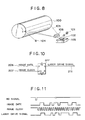
- Fig. 8 is a perspective view for explaining an image forming theory in a conventional image printing apparatus.
- This apparatus includes a photosensitive drum 100 serving as an electrostatic latent image carrier which is rotated at a constant speed in a direction indicated by an arrow.
- a semiconductor laser 101 outputs a laser beam 105 which is ON/OFF-modulated on the basis of print information input from a host computer (not shown) or the like.
- a polygonal mirror 102 is rotated by a scanner motor 103 at a predetermined speed to deflect the laser beam 105 incident through an optical system such as a collimator lens.
- a latent image is formed on the photosensitive drum 100 through a focusing lens 106 having f- ⁇ characteristics.
- a beam detector 104 receives the laser beam 105 scanned on the photosensitive drum 100 from the left to the right prior to scanning of an image write area and outputs a beam detection signal to a controller (not shown) to generate a horizontal sync signal BD which defines a write start position in the main scanning direction.
- the laser beam 105 modulated on the basis of image information is incident from the laser 101 to the photosensitive drum 100 serving as a latent image carrier through the rotating polygonal mirror 102.
- the laser beam 105 is scanned on the photosensitive drum 100 to form a latent image.
- the latent image is visualized into a toner image by a developing unit (not shown).
- the toner image is transferred to and fixed on a recording sheet, thereby forming an image.
- Fig. 9 is a control block diagram for explaining a control arrangement of the image printing apparatus shown in Fig. 8.
- a printer controller 200 develops image information received from a host computer or the like into a bit map in an internal memory. Image data 206 and an image clock 207 for latching this image data are output to a printer engine image control circuit 204 in synchronism with the BD signal 212 obtained from a printer engine BD signal detector 213. At the same time, the printer controller 200 performs serial communication with a print engine print control circuit 201 through a serial communication bus 205.
- a scanner driver 202 controls a scanner motor 103 shown in Fig. 8 and rotates it to a predetermined speed on the basis of a motor control signal 208 output from the print control circuit 201.
- a laser driver 203 controls emission of a laser beam from the semiconductor laser 101 (Fig. 8) on the basis of a laser control signal 209 output from the print control circuit 201.
- the image control circuit 204 receives image data 206 output in synchronism with the image clock 207 from the printer controller 200 and outputs a laser drive signal 211 to the laser driver 203.
- the image control circuit 204 receives an image control signal 210 from the print control circuit 201 and performs signal processing associated with resolution change-over.
- Fig. 10 is a block diagram of an arrangement of the image control circuit 204 (Fig. 9) which is exemplified by a D flip-flop DFF.
- Fig. 11 is a timing chart for explaining operations of the respective parts in Fig. 9, and the same reference numerals as in Fig. 9 denote the same parts in Fig. 11.
- the BD signal detector 213 shown in Fig. 9 When the beam detector 104 shown in Fig. 8 receives the laser beam 105, the BD signal detector 213 shown in Fig. 9 outputs the BD signal 212 to the printer controller 200.
- the image data 206 is output to the image control circuit 204 in synchronism with the image clock 207.
- the printer controller 200 serially transmits control information (e.g., a resolution change-over signal) to the print control circuit 201.
- the print control circuit 201 performs change-over processing such as speed change-over of the scanner driver 202. Therefore, an image can be printed at different resolutions in a single printing processor.
- Fig. 1 is a block diagram showing an arrangement of an image printing apparatus according to an embodiment of the present invention.
- the image printing apparatus comprises a printer controller 1 having a bit map memory for developing image information from a host computer into video information which is then sent to a printer engine.
- the printer controller 1 serially sends to print control circuit 2 print control information (e.g., a resolution change-over request) corresponding to bit information developed in the bit map memory.
- print control circuit 2 print control information (e.g., a resolution change-over request) corresponding to bit information developed in the bit map memory.
- the printer controller 1 In synchronism with a BD signal 14 sent from a BD signal detection circuit 5, the printer controller 1 also outputs to an image control circuit 6 an image clock 13 having one period corresponding to one pixel of an image and image data 12 output at a trailing edge of the image clock 13.
- the print control circuit 2 performs serial communication with the printer controller 1 and signals a state of the printer engine to the printer controller 1 and controls the printer engine state in response to a request such as a resolution change-over request from the printer controller 1.
- a resolution setting means 2a sets and changes over a frequency of the image clock 13 and a scanning speed of an optical scanning system in accordance with resolution information 10 corresponding to the image information (in this embodiment, a motor control signal 8 for changing a preset speed control constant of a scanner driver 3 is sent to the scanner driver 3).
- the resolution setting means 2a controls a scanner speed corresponding to the resolution. Note that the speed is increased as the resolution is increased.
- the print control circuit 2 sends the resolution information 10 to the image control circuit 6 which generates a laser drive signal 15.
- a duty ratio setting means 6a in the image control circuit 6 controls a signal duty ratio of one period of the image clock 13 for a laser ON period to be a value corresponding to the resolution.
- a light beam having an optimal light amount corresponding to the resolution is incident on the image carrier in units of pixels.
- a laser driver 4 causes to radiate on a photosensitive drum 100 a laser beam 105 ON/OFF-modulated by a laser control signal 9 and the laser drive signal 15 from the print control circuit 2.
- the image control circuit 6 receives an image control signal 11 output from the print control circuit 2 and performs signal processing associated with resolution change-over and change-over operations of the image clock 13.
- the printer controller 1 is connected to the print control circuit 2 through a serial communication bus 7.
- Fig. 2 is a circuit diagram for explaining an operation of the image control circuit 6 shown in Fig. 1.
- the same reference numerals as in Fig. 1 denote the same parts in Fig. 2.
- An 8-bit data bus consists of bit lines D0 to D7.
- the data bus outputs the resolution information 10 to a D/A converter COV.
- the D/A converter COV outputs a threshold voltage b for determining the signal duty ratio to one input terminal of comparator CMP.
- the image control circuit 6 also includes an gate circuit AND, a flip-flop FF1, resistors R1 to R5, capacitors C1 and C2, and amplifiers AMP1 and AMP2.
- the resistors R1 to R3, the amplifiers AMP1 and AMP2, and the like constitute a triangular wave generator ANG.
- a triangular wave c shown in Fig. 3 is input to the other input terminal of the comparator CMP.
- the input image data 12 is output from a port e to the flip-flop FF1.
- the image clock 13 is input to a terminal D of the flip-flop FF1, and a signal f is output from its terminal Q to the gate circuit AND.
- a gate output is output from a port g to the laser driver 4 as the laser drive signal 15.
- Fig. 3 is a timing chart for explaining the operation of the circuit arrangement of Fig. 2.
- the D/A converter COV When the resolution information 10 is signaled to the image control circuit 6 through the data bus (D0 to D7) shown in Fig. 2, the D/A converter COV outputs a triangular wave threshold voltage Vs for setting the signal duty ratio to the comparator CMP through a line b .
- the triangular wave (c) input to the comparator CMP is waveshaped by a threshold voltage (b) shown in Fig. 3, thereby obtaining the image clock 13(d) representing a signal duty corresponding to the resolution information 10.
- the image data 12(e) is latched by the flip-flop FF1 at a leading edge of the image clock 13(a) and is output from the terminal Q to the gate circuit AND.
- the gate circuit AND outputs the laser drive signal 15 from its port g to the laser driver 4.
- the laser drive signal 15 is obtained by ANDing the signal f and the image clock (signal at the port d ) having a signal duty ratio corresponding to the resolution information 10.
- the laser drive signal 15 based on the conventional signal f becomes the laser drive signal 15 output from the port g . It is therefore possible to turn on the laser within a shorter period of time by one period of the image clock 13.
- the image data 12 output from the printer controller 1 is serially processed line by line by the image control circuit 6.
- the present invention is applicable to an apparatus for parallelly performing read and write access of the image data 12 by arranging a plurality of line buffers 17 and 18.
- Fig. 4 is a block diagram of an image printing apparatus according to another embodiment of the present invention.
- the same reference numerals as in Fig. 1 denote the same parts in Fig. 4.
- a write control circuit 16 sets the line buffer 17 or 18 in a write state in response to a write control signal 20 output from a print control circuit 2.
- the line buffers 17 and 18 constitute a toggle circuit in which one line buffer is set in a read state while the other line buffer is set in a write state, and vice versa.
- a read control circuit 19 sets the either the line buffer 17 or 18 in a read state in response to a read control signal 21 output from the print control circuit 2.
- the read control circuit 19 changes over a signal duty ratio of one period of an image clock 13 on the basis of resolution information 22 output from the print control circuit 2.
- This image printing apparatus generates write data 23 and 24, read data 25 and 26, and a transfer clock 27.
- Fig. 5 is a block diagram showing a detailed arrangement of the read control circuit 19 shown in Fig. 4.
- the same reference numerals as in Fig. 4 denote the same parts in Fig. 5.
- the read control circuit 19 includes image clock Xn oscillators 31-1 to 31-N for generating clocks having frequencies corresponding to recording resolutions, i.e., generate clock signals having frequencies (n times of the frequency of the image clock 13; eight times in this embodiment) corresponding to the resolutions.
- the resolutions are 300 DPI, 400 DPI, and 600 DPI.
- a decoder 32 decodes resolution data having bits D0 to D2 designated by resolution information 10 and selects one of the oscillators 31-1 to 31-N.
- a read clock generator 33 receives a BD signal 14 through a BD signal generator 41, counts 8-time image clocks from the leading edge by a predetermined number (3 in the embodiment shown in Fig. 6), and starts to frequency-divide the clock, thereby obtaining an image clock 33a.
- An internal counter in a duty change-over clock generator 34 counts the selected 8-time image clocks by a complement of a 3-bit value, and is then reset to input a duty change-over clock 34a having a larger duty ratio of the image clock to a gate circuit 43.
- Shift registers 35 and 36 read out image data 12 stored in line buffers 17 and 18 in synchronism with a read clock from the clock generator 33.
- the readout image data is output to the gate circuit 43 through a gate circuit 42.
- a shift register 37 writes the image data 12 sent from a printer controller 1 in the line buffers 17 and 18 in synchronism with the transfer clock 27.
- a frequency divider 38 outputs a clock obtained by frequency-dividing the transfer lock 27 to the line buffers 17 and 18.
- a frequency divider 39 outputs a clock obtained by frequency-dividing the image clock 33a to the line buffers 17 and 18.
- a chip selector 40 controls read/write enable states of the line buffers 17 and 18.
- the BD signal generator 41 waveshapes the input BD signal 14 and outputs a horizontal sync signal to the respective parts.
- Fig. 6 is a timing chart for explaining an operation of the circuit arrangement shown in Fig. 5.
- the internal counter in the duty change-over clock generator 34 counts 8-time image clocks by a complement of a 3-bit value in accordance with the resolution data (D0 to D2) and is then reset to generate the duty change-over clock 34a.
- the duty change-over clock 34a is output to the gate circuit 43.
- the duty of the image clock 13 defined by one of the oscillators 31-1 to 31-N which is selected by the resolution is changed over, thereby obtaining the laser drive signal 15 based on the image data.
- the duty change-over clock 34a is generated by the read control circuit 19.
- the duty change-over clock may be generated by an internal clock circuit in a printer controller 1.
- Fig. 7 is a block diagram showing an arrangement of an image printing apparatus according to still another embodiment of the present invention.
- the same reference numerals as in Fig. 1 denote the same parts in Fig. 7.
- a duty change-over clock 50 is generated by an internal clock circuit in a printer controller 1 and is output to an image control circuit 6.
- the printer controller 1 analyzes image information input from a host computer and generates the duty change-over clock 50 corresponding to a desired resolution when the resolution change-over operation is required and is output to the image control circuit 6.
- image data 12 is output to the image control circuit 6 in synchronism with an image clock 13 and is ANDed with the duty change-over clock 50 to obtain laser drive signal 15.
- the laser drive signal 15 is output to a laser driver 4. Therefore, modifications of a conventional circuit can be minimized, and the laser drive signal 15 corresponding to the desired resolution can be generated and output at low cost.
- a resolution setting means for setting and changing over a frequency of an image clock signal and a scanning speed of an optical scanning system in accordance with resolution information designated by image information and a duty ratio setting means for changing over a signal duty ratio of the image clock signal having a predetermined frequency set by the resolution setting means in accordance with the designated resolution.
- a light beam ON time for one pixel can be optimally set without changing a beam spot size while the image clock is changed over in correspondence with the resolution.
- the image quality of a thin line image can be greatly improved as compared with an image based on the conventional image clock. Therefore, the line width of an image during formation of a vertical line image will not be increased, and thin lines such as a table image serving as a format image and rulers can be drawn, thus providing many practical advantages.
Landscapes
- Engineering & Computer Science (AREA)
- Multimedia (AREA)
- Signal Processing (AREA)
- Physics & Mathematics (AREA)
- Optics & Photonics (AREA)
- General Engineering & Computer Science (AREA)
- General Physics & Mathematics (AREA)
- Theoretical Computer Science (AREA)
- Laser Beam Printer (AREA)
- Fax Reproducing Arrangements (AREA)
- Mechanical Optical Scanning Systems (AREA)
- Dot-Matrix Printers And Others (AREA)
Applications Claiming Priority (2)
| Application Number | Priority Date | Filing Date | Title |
|---|---|---|---|
| JP1223113A JPH0387773A (ja) | 1989-08-31 | 1989-08-31 | 画像印字装置 |
| JP223113/89 | 1989-08-31 |
Publications (3)
| Publication Number | Publication Date |
|---|---|
| EP0415725A2 true EP0415725A2 (de) | 1991-03-06 |
| EP0415725A3 EP0415725A3 (en) | 1992-06-10 |
| EP0415725B1 EP0415725B1 (de) | 1996-03-06 |
Family
ID=16793028
Family Applications (1)
| Application Number | Title | Priority Date | Filing Date |
|---|---|---|---|
| EP90309416A Expired - Lifetime EP0415725B1 (de) | 1989-08-31 | 1990-08-29 | Bildaufzeichnungsgerät |
Country Status (4)
| Country | Link |
|---|---|
| US (1) | US5262801A (de) |
| EP (1) | EP0415725B1 (de) |
| JP (1) | JPH0387773A (de) |
| DE (1) | DE69025679D1 (de) |
Cited By (2)
| Publication number | Priority date | Publication date | Assignee | Title |
|---|---|---|---|---|
| EP0533592A3 (en) * | 1991-09-20 | 1993-09-15 | Eastman Kodak Company | Apparatus and method for thermal printing of finely detailed images of photographic quality |
| EP0574249A1 (de) * | 1992-06-12 | 1993-12-15 | Xerox Corporation | Auf einem Halbleitersubstrat herstellbares intelligentes Lasersystem mit programmierbarer Intensität |
Families Citing this family (9)
| Publication number | Priority date | Publication date | Assignee | Title |
|---|---|---|---|---|
| US5450121A (en) * | 1991-12-20 | 1995-09-12 | Compaq Computer Corporation | Margin control for laser printers |
| EP0416832B1 (de) * | 1989-09-07 | 1996-07-10 | Canon Kabushiki Kaisha | Bilddarstellungsgerät |
| JP3226595B2 (ja) * | 1992-04-23 | 2001-11-05 | キヤノン株式会社 | 記録装置および記録回路ユニット |
| JPH08160828A (ja) * | 1994-12-07 | 1996-06-21 | Canon Inc | 電子写真プリンタ |
| JP4333971B2 (ja) | 1998-11-11 | 2009-09-16 | キヤノン株式会社 | 画像処理システム |
| JP2002072638A (ja) | 2000-06-13 | 2002-03-12 | Canon Inc | 画像形成装置 |
| JP2004341295A (ja) * | 2003-05-16 | 2004-12-02 | Hitachi Printing Solutions Ltd | 電子写真装置の露光装置 |
| US20050206719A1 (en) * | 2004-03-22 | 2005-09-22 | Kabushiki Kaisha Toshiba | Image forming apparatus |
| US20050254085A1 (en) * | 2004-05-12 | 2005-11-17 | Koji Oshikiri | Image forming system |
Family Cites Families (3)
| Publication number | Priority date | Publication date | Assignee | Title |
|---|---|---|---|---|
| US4799069A (en) * | 1986-04-18 | 1989-01-17 | Minolta Camera Kabushiki Kaisha | Laser recording apparatus |
| JPS62280040A (ja) * | 1986-05-30 | 1987-12-04 | Toshiba Corp | 画像形成装置 |
| JP2589295B2 (ja) * | 1986-11-14 | 1997-03-12 | キヤノン株式会社 | 画像形成装置 |
-
1989
- 1989-08-31 JP JP1223113A patent/JPH0387773A/ja active Pending
-
1990
- 1990-08-28 US US07/573,686 patent/US5262801A/en not_active Expired - Lifetime
- 1990-08-29 EP EP90309416A patent/EP0415725B1/de not_active Expired - Lifetime
- 1990-08-29 DE DE69025679T patent/DE69025679D1/de not_active Expired - Lifetime
Cited By (2)
| Publication number | Priority date | Publication date | Assignee | Title |
|---|---|---|---|---|
| EP0533592A3 (en) * | 1991-09-20 | 1993-09-15 | Eastman Kodak Company | Apparatus and method for thermal printing of finely detailed images of photographic quality |
| EP0574249A1 (de) * | 1992-06-12 | 1993-12-15 | Xerox Corporation | Auf einem Halbleitersubstrat herstellbares intelligentes Lasersystem mit programmierbarer Intensität |
Also Published As
| Publication number | Publication date |
|---|---|
| EP0415725A3 (en) | 1992-06-10 |
| JPH0387773A (ja) | 1991-04-12 |
| DE69025679D1 (de) | 1996-04-11 |
| US5262801A (en) | 1993-11-16 |
| EP0415725B1 (de) | 1996-03-06 |
Similar Documents
| Publication | Publication Date | Title |
|---|---|---|
| US5124802A (en) | Electrostatic lasar printer with a short side length of a modulation area formed by pulse width modulation set relative to a detected toner particle size | |
| US5982508A (en) | Image processing method and apparatus | |
| US4905022A (en) | Image forming apparatus having laser light source | |
| US5742317A (en) | Image processing apparatus and recording apparatus | |
| US5262801A (en) | Image recording apparatus | |
| US5517318A (en) | Image forming apparatus | |
| US6570672B1 (en) | Printing system and method | |
| US5249060A (en) | Using horizontal and vertical synchronization signals to exclude inhibiting printing in an area defined by necessary description area data | |
| JP3409889B2 (ja) | 記録制御装置 | |
| JPH07156443A (ja) | 画像形成装置 | |
| JPH04369968A (ja) | 2値画像形成装置 | |
| JPH09174937A (ja) | 画像形成装置および方法 | |
| JP2989222B2 (ja) | 画像記録装置 | |
| US6850343B1 (en) | System and method for scanner control using thinning-out processing | |
| JP2950829B2 (ja) | デジタルカラー画像形成装置 | |
| JP2901062B2 (ja) | 画像形成装置 | |
| JP2721347B2 (ja) | 画像処理装置 | |
| US5737093A (en) | Recording data generating device having output allowance/prevention mode | |
| JPH0596780A (ja) | 画像記録装置 | |
| JPH04351065A (ja) | 2値画像形成装置 | |
| JPH03193380A (ja) | 画像形成装置 | |
| JPH09123522A (ja) | 電子写真記録装置 | |
| JPH04326854A (ja) | 2値画像形成装置 | |
| JPH04326855A (ja) | 2値画像形成装置 | |
| JP2000301768A (ja) | 印刷方法及び印刷装置 |
Legal Events
| Date | Code | Title | Description |
|---|---|---|---|
| PUAI | Public reference made under article 153(3) epc to a published international application that has entered the european phase |
Free format text: ORIGINAL CODE: 0009012 |
|
| 17P | Request for examination filed |
Effective date: 19901231 |
|
| AK | Designated contracting states |
Kind code of ref document: A2 Designated state(s): DE FR GB IT |
|
| PUAL | Search report despatched |
Free format text: ORIGINAL CODE: 0009013 |
|
| AK | Designated contracting states |
Kind code of ref document: A3 Designated state(s): DE FR GB IT |
|
| 17Q | First examination report despatched |
Effective date: 19940701 |
|
| GRAA | (expected) grant |
Free format text: ORIGINAL CODE: 0009210 |
|
| AK | Designated contracting states |
Kind code of ref document: B1 Designated state(s): DE FR GB IT |
|
| PG25 | Lapsed in a contracting state [announced via postgrant information from national office to epo] |
Ref country code: IT Free format text: LAPSE BECAUSE OF FAILURE TO SUBMIT A TRANSLATION OF THE DESCRIPTION OR TO PAY THE FEE WITHIN THE PRE;WARNING: LAPSES OF ITALIAN PATENTS WITH EFFECTIVE DATE BEFORE 2007 MAY HAVE OCCURRED AT ANY TIME BEFORE 2007. THE CORRECT EFFECTIVE DATE MAY BE DIFFERENT FROM THE ONE RECORDED.SCRIBED TIME-LIMIT Effective date: 19960306 Ref country code: FR Effective date: 19960306 |
|
| REF | Corresponds to: |
Ref document number: 69025679 Country of ref document: DE Date of ref document: 19960411 |
|
| PG25 | Lapsed in a contracting state [announced via postgrant information from national office to epo] |
Ref country code: DE Effective date: 19960608 |
|
| EN | Fr: translation not filed | ||
| PLBE | No opposition filed within time limit |
Free format text: ORIGINAL CODE: 0009261 |
|
| STAA | Information on the status of an ep patent application or granted ep patent |
Free format text: STATUS: NO OPPOSITION FILED WITHIN TIME LIMIT |
|
| 26N | No opposition filed | ||
| REG | Reference to a national code |
Ref country code: GB Ref legal event code: IF02 |
|
| PGFP | Annual fee paid to national office [announced via postgrant information from national office to epo] |
Ref country code: GB Payment date: 20080814 Year of fee payment: 19 |
|
| GBPC | Gb: european patent ceased through non-payment of renewal fee |
Effective date: 20090829 |
|
| PG25 | Lapsed in a contracting state [announced via postgrant information from national office to epo] |
Ref country code: GB Free format text: LAPSE BECAUSE OF NON-PAYMENT OF DUE FEES Effective date: 20090829 |