EP0418733A2 - Mélange polymérisable par radiation et procédé de préparation d'une masque pour soudage - Google Patents
Mélange polymérisable par radiation et procédé de préparation d'une masque pour soudage Download PDFInfo
- Publication number
- EP0418733A2 EP0418733A2 EP19900117636 EP90117636A EP0418733A2 EP 0418733 A2 EP0418733 A2 EP 0418733A2 EP 19900117636 EP19900117636 EP 19900117636 EP 90117636 A EP90117636 A EP 90117636A EP 0418733 A2 EP0418733 A2 EP 0418733A2
- Authority
- EP
- European Patent Office
- Prior art keywords
- radiation
- mixture according
- weight
- methacrylic acid
- polymerizable mixture
- Prior art date
- Legal status (The legal status is an assumption and is not a legal conclusion. Google has not performed a legal analysis and makes no representation as to the accuracy of the status listed.)
- Granted
Links
Images
Classifications
-
- H—ELECTRICITY
- H05—ELECTRIC TECHNIQUES NOT OTHERWISE PROVIDED FOR
- H05K—PRINTED CIRCUITS; CASINGS OR CONSTRUCTIONAL DETAILS OF ELECTRIC APPARATUS; MANUFACTURE OF ASSEMBLAGES OF ELECTRICAL COMPONENTS
- H05K3/00—Apparatus or processes for manufacturing printed circuits
- H05K3/22—Secondary treatment of printed circuits
- H05K3/28—Applying non-metallic protective coatings
- H05K3/285—Permanent coating compositions
- H05K3/287—Photosensitive compositions
-
- G—PHYSICS
- G03—PHOTOGRAPHY; CINEMATOGRAPHY; ANALOGOUS TECHNIQUES USING WAVES OTHER THAN OPTICAL WAVES; ELECTROGRAPHY; HOLOGRAPHY
- G03F—PHOTOMECHANICAL PRODUCTION OF TEXTURED OR PATTERNED SURFACES, e.g. FOR PRINTING, FOR PROCESSING OF SEMICONDUCTOR DEVICES; MATERIALS THEREFOR; ORIGINALS THEREFOR; APPARATUS SPECIALLY ADAPTED THEREFOR
- G03F7/00—Photomechanical, e.g. photolithographic, production of textured or patterned surfaces, e.g. printing surfaces; Materials therefor, e.g. comprising photoresists; Apparatus specially adapted therefor
- G03F7/004—Photosensitive materials
-
- C—CHEMISTRY; METALLURGY
- C08—ORGANIC MACROMOLECULAR COMPOUNDS; THEIR PREPARATION OR CHEMICAL WORKING-UP; COMPOSITIONS BASED THEREON
- C08F—MACROMOLECULAR COMPOUNDS OBTAINED BY REACTIONS ONLY INVOLVING CARBON-TO-CARBON UNSATURATED BONDS
- C08F257/00—Macromolecular compounds obtained by polymerising monomers on to polymers of aromatic monomers as defined in group C08F12/00
- C08F257/02—Macromolecular compounds obtained by polymerising monomers on to polymers of aromatic monomers as defined in group C08F12/00 on to polymers of styrene or alkyl-substituted styrenes
-
- C—CHEMISTRY; METALLURGY
- C08—ORGANIC MACROMOLECULAR COMPOUNDS; THEIR PREPARATION OR CHEMICAL WORKING-UP; COMPOSITIONS BASED THEREON
- C08F—MACROMOLECULAR COMPOUNDS OBTAINED BY REACTIONS ONLY INVOLVING CARBON-TO-CARBON UNSATURATED BONDS
- C08F283/00—Macromolecular compounds obtained by polymerising monomers on to polymers provided for in subclass C08G
- C08F283/10—Macromolecular compounds obtained by polymerising monomers on to polymers provided for in subclass C08G on to polymers containing more than one epoxy radical per molecule
-
- G—PHYSICS
- G03—PHOTOGRAPHY; CINEMATOGRAPHY; ANALOGOUS TECHNIQUES USING WAVES OTHER THAN OPTICAL WAVES; ELECTROGRAPHY; HOLOGRAPHY
- G03F—PHOTOMECHANICAL PRODUCTION OF TEXTURED OR PATTERNED SURFACES, e.g. FOR PRINTING, FOR PROCESSING OF SEMICONDUCTOR DEVICES; MATERIALS THEREFOR; ORIGINALS THEREFOR; APPARATUS SPECIALLY ADAPTED THEREFOR
- G03F1/00—Originals for photomechanical production of textured or patterned surfaces, e.g., masks, photo-masks, reticles; Mask blanks or pellicles therefor; Containers specially adapted therefor; Preparation thereof
- G03F1/20—Masks or mask blanks for imaging by charged particle beam [CPB] radiation, e.g. by electron beam; Preparation thereof
-
- G—PHYSICS
- G03—PHOTOGRAPHY; CINEMATOGRAPHY; ANALOGOUS TECHNIQUES USING WAVES OTHER THAN OPTICAL WAVES; ELECTROGRAPHY; HOLOGRAPHY
- G03F—PHOTOMECHANICAL PRODUCTION OF TEXTURED OR PATTERNED SURFACES, e.g. FOR PRINTING, FOR PROCESSING OF SEMICONDUCTOR DEVICES; MATERIALS THEREFOR; ORIGINALS THEREFOR; APPARATUS SPECIALLY ADAPTED THEREFOR
- G03F7/00—Photomechanical, e.g. photolithographic, production of textured or patterned surfaces, e.g. printing surfaces; Materials therefor, e.g. comprising photoresists; Apparatus specially adapted therefor
- G03F7/004—Photosensitive materials
- G03F7/027—Non-macromolecular photopolymerisable compounds having carbon-to-carbon double bonds, e.g. ethylenic compounds
- G03F7/032—Non-macromolecular photopolymerisable compounds having carbon-to-carbon double bonds, e.g. ethylenic compounds with binders
- G03F7/033—Non-macromolecular photopolymerisable compounds having carbon-to-carbon double bonds, e.g. ethylenic compounds with binders the binders being polymers obtained by reactions only involving carbon-to-carbon unsaturated bonds, e.g. vinyl polymers
-
- H—ELECTRICITY
- H05—ELECTRIC TECHNIQUES NOT OTHERWISE PROVIDED FOR
- H05K—PRINTED CIRCUITS; CASINGS OR CONSTRUCTIONAL DETAILS OF ELECTRIC APPARATUS; MANUFACTURE OF ASSEMBLAGES OF ELECTRICAL COMPONENTS
- H05K2203/00—Indexing scheme relating to apparatus or processes for manufacturing printed circuits covered by H05K3/00
- H05K2203/07—Treatments involving liquids, e.g. plating, rinsing
- H05K2203/0779—Treatments involving liquids, e.g. plating, rinsing characterised by the specific liquids involved
- H05K2203/0786—Using an aqueous solution, e.g. for cleaning or during drilling of holes
- H05K2203/0793—Aqueous alkaline solution, e.g. for cleaning or etching
-
- Y—GENERAL TAGGING OF NEW TECHNOLOGICAL DEVELOPMENTS; GENERAL TAGGING OF CROSS-SECTIONAL TECHNOLOGIES SPANNING OVER SEVERAL SECTIONS OF THE IPC; TECHNICAL SUBJECTS COVERED BY FORMER USPC CROSS-REFERENCE ART COLLECTIONS [XRACs] AND DIGESTS
- Y10—TECHNICAL SUBJECTS COVERED BY FORMER USPC
- Y10S—TECHNICAL SUBJECTS COVERED BY FORMER USPC CROSS-REFERENCE ART COLLECTIONS [XRACs] AND DIGESTS
- Y10S430/00—Radiation imagery chemistry: process, composition, or product thereof
- Y10S430/136—Coating process making radiation sensitive element
Definitions
- the invention relates to a radiation-polymerizable mixture which is used for the production of solder mask.
- solder mask on printed circuit boards using the photoresist technique.
- photoresist solutions are applied to the structured printed circuit board, dried and imagewise hardened by exposure at the points where the printed circuit board is to be covered.
- the solder mask is obtained by washing out the unexposed layer areas.
- the photoresist layer can also be applied to the printed circuit board by the dry resist method by laminating a prefabricated thermoplastic layer.
- Suitable materials for the production of solder mask are e.g. B. described in DE-A 27 47 947. These are photopolymerizable layers which contain a certain amount of bound halogen to improve the flame resistance.
- a similar material is described in EP-A 15 004, which can be developed dry by mechanical separation of exposed and unexposed layer areas ("peel-apart method").
- EP-A 2040 describes a light-curable material intended for the same purpose Material described in which certain epoxy resins are used as photosensitive compounds.
- EP-B 0 113 409 a light-sensitive layer is applied over a screen printing stencil, so the photopolymerization is only used for mask hardening and is not used for image generation.
- US Pat. No. 3,776,729 describes a mixture consisting mainly of photopolymerizable acrylates and thermally crosslinkable epoxides. A mask made from this mixture is developed after imagewise UV exposure in organic solvents (e.g. butanone) and cured by heating.
- organic solvents e.g. butanone
- EP-A 0 273 729 describes a light-sensitive, aqueous-alkaline developable mixture for solder mask, which is essentially produced by reacting epoxidized phenolic resins with acrylic acid and maleic anhydride. The reaction product no longer contains epoxy groups.
- the aqueous alkaline developability of an exposed mask is achieved by copolymers which contain N-isobutoxymethylacrylamide and methacrylic acid as co-components.
- the solder mask obtained can be post-cured thermally, but requires relatively long curing times at relatively high temperatures.
- a bis-epoxy compound is added to the photopolymerizable mixture for the production of the solder mask and the light-cured image template is hardened after development by heating. This process produces very temperature-resistant solder mask. However, the mixture contains no inorganic pigment.
- EP-A 73 444 describes similar mixtures which have a good shelf life in the unexposed state.
- the mixtures contain compounds with the binder, the polymerization product of the ethylenically unsaturated compound and / or with itself are thermally crosslinkable.
- Those compounds are preferably used which contain epoxy groups or groups of the formula -CH2-OR as crosslinking groups, in which R is a hydrogen atom, a lower alkyl, acyl or hydroxyalkyl group and in which the groups -CH2OR are open-chain on a nitrogen atom of a low molecular weight or cyclic acid amides or on an aromatic carbon atom of a compound capable of condensation with formaldehyde.
- the object of the invention was to propose suitable photopolymerizable mixtures for the production of thermally curable solder mask, which are in the form have a solution or dispersion applied to the base, which have a high solids content, which show a good course in all customary coating processes, which have good drying behavior, high photosensitivity, high resolution and good soldering behavior, which are found in purely aqueous, alkaline media can be developed and solder masks with good mechanical, chemical and electrical properties result.
- a method for producing a solder mask is further proposed, which is characterized in that a solution or dispersion of a mixture of the above-mentioned composition is applied to the surface of a printed circuit and dried, the layer obtained imagewise with actinic radiation, with the soldering eyes being excluded irradiated, the unirradiated layer areas washed out with a developer and the solder mask obtained heated to an elevated temperature.
- esters of acrylic or methacrylic acid with polyhydric preferably primary, alcohols are generally used.
- the alcohol should contain at least two hydroxyl groups, since the desired crosslinking effect is achieved by polyunsaturated compounds.
- a minor amount of esters of monohydric alcohols can also be present in the mixture.
- suitable polyhydric alcohols are ethylene glycol, propylene glycol, 1,4-butanediol, diethylene glycol, triethylene glycol, oligopropylene glycols, trimethylolethane and propane, pentaerythritol, dipentaerythritol, bisphenol-A-bis-hydroxyethyl ether.
- the low molecular weight, urethane-containing bis-acrylates and bismethacrylates are also suitable, which by reacting 2 mol of hydroxyalkyl acrylate or methacrylate with 1 mol of an aliphatic or cycloaliphatic diisocyanate, e.g. B. 2,2,4-trimethyl-hexamethylene diisocyanate can be obtained.
- an aliphatic or cycloaliphatic diisocyanate e.g. B. 2,2,4-trimethyl-hexamethylene diisocyanate
- Such monomers containing urethane groups are described in US Pat. No. 4,088,498.
- Acrylates and methacrylates, in particular acrylates, with a high double bond content are particularly advantageous.
- Monomers with 3 or more unsaturated groups are preferred.
- esters are still at least one free hydroxy group included, superior to the fully esterified compounds.
- esters of trimethylolpropane, trimethylolethane, pentaerythritol and dipentaerythritol are particularly preferred.
- the monomer is generally present in the mixture in an amount of from 10 to 35, preferably from up to 30,% by weight, based on the total content of nonvolatile constituents.
- the polymeric binder is essential for the usability of the mixture according to the invention. It usually consists of three components: methacrylic acid, a methacrylic acid ester and a styrene. Units of additional monomers such as acrylic acid, acrylic acid ester, acrylonitrile or methacrylonitrile, acrylic or methacrylamide or vinyl heterocycles can also be present in a smaller amount. Alkyl esters with preferably 1 to 10, in particular 1 to 7, carbon atoms are used as methacrylic acid esters in the alkyl group.
- the styrene can be an o-, m- or p-vinyl toluene, a vinyl ethylbenzene, the ⁇ -methyl or ⁇ -chlorostyrene, an o-, m- or p-chlorostyrene, a vinyl anisole or the like.
- the unsubstituted styrene is generally preferred.
- the proportion of styrene units is in the range from up to 65, preferably from 45 to 55% by weight; that of the methacrylic acid ester at 5 to 40, preferably between and 25 wt .-%.
- the methacrylic acid units should be present in such an amount that the acid number of the polymer is in the range from 110 to 280, preferably from 125 to 260.
- the proportion of the styrene compound must be in the range given in order to achieve good soldering stability.
- the proportion of the polymer in the mixture is generally 15 to 50, preferably up to 40,% by weight.
- Silicates or silicas are suitable as mineral pigments. They should be ground to a particle size such that at least 90% of the particles have a diameter of 5 ⁇ m or less. This gives the solder mask a smooth surface. These silicate minerals contain practically all chemically bound water in the form of OH groups on the silicon.
- OH groups are important; they allow cross-linking with the epoxides described below which is favorable for the mechanical properties of the mask.
- the following can be used: silica, feldspar, anphibole, serpentine, zeolite, pumice and phonolite.
- the SiO2 content is usually above 60%.
- Aluminum, alkaline earth and alkali metals advantageously act as counterions contained in the crystal structure.
- the amount of pigment is generally about 20 to 50, preferably 25 to 40 wt .-%.
- polymerization initiators which can be activated by radiation.
- examples are benzoins, benzoin ethers, multinuclear quinones such as 2-ethylanthraquinone, acridine derivatives such as 9-phenylacridine or benzacridines, phenazine derivatives such as 9,10-dimethylbenz (a) phenazine, quinoxaline or quinoline derivatives such as 2,3-bis- (4- methoxyphenyl) quinoxaline or 2-styrylquinoline, quinazoline compounds or acylphosphine oxide compounds.
- Photoinitiators of this kind are described in DE-C 20 27 467, 20 39 861, DE-A 37 28 168, EP-B 11 786 and EP-A 220 589.
- mercapto compounds e.g. As hydrazone, mercapto compounds, pyrylium or thiopyrylium salts, xanthones, thioxanthones, benzoquinones, acetophenones, benzophenones, synergistic mixtures with ketones or hydroxyketones and dye redox systems can be used.
- Photoinitiators which have light-cleavable trihalomethyl groups are particularly preferred, corresponding compounds from the triazine or thiazoline series being mentioned in particular. Such compounds are described in DE-A 27 18 259, 33 33 450 and 33 37 024.
- a preferred example is 2- (4-methoxystyryl) 4,6-bis-trichloromethyl-s-triazine.
- the photoinitiators are generally added in amounts of from 0.1 to 15, preferably from 0.5 to 10,% by weight, based on the nonvolatile constituents of the mixture.
- the mixture according to the invention also contains di- or polyvalent epoxy compounds.
- di- or polyvalent epoxy compounds examples include bisglycidyl ethers of dihydric alcohols and phenols, e.g. B. of bisphenol A, of polyethylene glycol and polypropylene glycol ethers of bisphenol A, of butane-1,4-diol, hexane-1,6-diol, polyethylene glycol, polypropylene glycol or polytetrahydrofuran.
- Bisglycidyl ether of trihydric alcohols e.g. B. of glycerin
- the epoxides are usually added to the mixture in an amount of about 10 to 30, preferably 12 to 25% by weight, based on the non-volatile constituents of the mixture.
- Bisepoxides of the general formula are preferred used where Z is an alkylene or hydroxyalkylene group having 2 to 6 carbon atoms or the group R1 represents a hydrogen atom or a methyl group, n1 and n2 numbers from 0 to 10, preferably from 0 to 5, and n3 0 or a number from 1 to 4, preferably 0 or 1, mean.
- Particularly suitable tris and polyfunctional epoxides are epoxidized phenol-formaldehyde resins with chain links of the general formula: where n is an integer that is at least 2.
- the mixture contains a hardener or addition initiator for epoxy groups.
- the hardener is preferably a nitrogen base, e.g. B. triethylamine, 1,4-diazabicyclo [2.2.2] octane (Dabco), dibutylamine, more alkylated mono-, di- and triamines on an aliphatic basis, also aliphatic-aromatic amines such as. B. Dimethylaniline.
- the tertiary, especially aliphatic amines are preferred. Diazabicyclooctane is very particularly preferred.
- the amount of base is generally between 0.15 and 1.5, preferably between 0.2 and 1.0% by weight.
- the mixture preferably contains at least one dye in order to make the developed resist template more visible. It is advantageous to use a combination of at least two dyes, one of which changes its color when irradiated and destroys it at temperatures above 200 ° C. H. becomes colorless. The other dye should survive both the radiation and temperatures above 200 ° C without change. It should make the solder mask clearly visible during and after soldering. Dyes suitable for this are described in DE-A 3 114 931.
- the mixture may optionally contain a number of other common additives, e.g. B. inhibitors to prevent thermal polymerization of the monomers, hydrogen donors, sensitometric regulators, pigments, plasticizers and thixotropic agents, in particular mineral pigments such as SiO2, or organic polymers such as polyacrylamides.
- B. inhibitors to prevent thermal polymerization of the monomers hydrogen donors, sensitometric regulators, pigments, plasticizers and thixotropic agents, in particular mineral pigments such as SiO2, or organic polymers such as polyacrylamides.
- Thixotropic agents are e.g. B. advantageous when applying by screen printing.
- the mixture according to the invention has a limited shelf life in the form ready for processing; therefore, the individual components are suitably stored separately in at least two containers - "two-component lacquer".
- the normal procedure is that all components, with the exception of the epoxy compound, are present in a main mixture to which the epoxy is added shortly before processing. But you can also z. B. keep the curing initiator as a separate component. Dyes, mineral solids and other additives can also be present in separate mixed components, so that, if appropriate, a three-component system can be formulated. It is important that the partial mixtures have a sufficiently long shelf life (approx. 6 to 12 months) before the mixing process.
- the mixture according to the invention is processed in a known manner, e.g. B. in the screen application.
- the dissolved or dispersed mixture is z. B. applied by a screen fabric stretched in a metal frame of 37 to 55 meshes per cm with a squeegee on the circuit board object.
- Another option is curtain coating. With the help of a commercially available curtain casting machine, a continuously vertical liquid film is produced. The circuit board is passed under this film by means of a conveyor belt and coated with it.
- the mixture can also be applied via an electrostatic spray coating. In a closed cabin, the solution is broken up into fine droplets on a spray head, these are electrostatically charged by high voltage and deposited on the circuit board.
- the mixtures can also be processed using the dip-drawing process and roller application.
- the coating mixtures processed according to one of the processes described are freed from the solvent by drying in a forced-air drying cabinet or under an IR dryer.
- the printed circuit board coated in this way is then exposed through a template which protects the parts of the board from the radiation which must remain free for the soldering process.
- any electromagnetic radiation whose energy is sufficient to excite a suitable polymerization initiator can be considered as actinic radiation, to which the mixture according to the invention is sensitive. Visible and ultraviolet light, X-rays, ⁇ and electron radiation are particularly suitable. Laser radiation in the visible and UV range can also be used. Short-wave visible and close UV light is preferred.
- Aqueous, preferably aqueous-alkaline solutions e.g. B. of alkali metal phosphates, carbonates or silicates, suitable, which may contain small amounts, eg. B. up to 10 wt .-% of water-miscible organic solvents or wetting agents can be added.
- the good mechanical, thermal and chemical properties of the solder mask are brought about by the thermal aftertreatment.
- This ther Mixing treatment is generally between 80 ° C and 150 ° C, with approximate treatment times of 10 to 60 minutes.
- the ready-to-solder plate can then be equipped with electronic components in a known manner.
- the line side of the plate is then usually treated with a suitable, commercially available flux and subjected to the wave soldering using a commercially available wave soldering machine.
- a suitable, commercially available flux and subjected to the wave soldering using a commercially available wave soldering machine.
- Known eutectic mixtures which allow soldering temperatures of approximately 230 to 260 ° C. are used as the solder.
- a known mixture contains, for example, 63% by weight of tin and 37% by weight of lead.
- the solder mask made according to the invention can be used successfully.
- the mixtures according to the invention result in solder resist layers which are distinguished by high flexibility and mechanical strength in the unexposed and exposed state and by high temperature resistance in the exposed and post-cured state.
- the photopolymerizable layers have high photosensitivity and result in good curing or crosslinking even with a high layer thickness.
- the exposed layers can be developed perfectly and completely with aqueous-alkaline solutions, even with layer thicknesses above 100 ⁇ m.
- the exposed and developed layers can be thermally hardened without unduly affecting the flexibility of the mask or its adhesion to the base and without changing the position and dimensions of the areas exposed by development.
- the hardened masks are resistant to atmospheric, thermal and chemical influences over long periods. After exposure of the resist layer, a high-contrast image is obtained in the layer.
- the solder mask obtained from the mixtures according to the invention are particularly suitable for effectively and permanently protecting sensitive electronic conductor structures from atmospheric attacks.
- the reduced specific viscosity of the product was 0.185 dl / g (measured on a 1% solution in dimethylformamide at 25 ° C).
- 3-methoxy-butanol-1 112.5 pbw of pentaerythritol triacrylate, 128.9 pbw of trimethylolpropane triacrylate, 27.5 pbw of 9-phenylacridine, 12.4 pbw neozapone green, 1.2 pbw of a blue azo dye obtained by coupling 2,4-dinitro-6-chloro-benzenediazonium salt with 2-methoxy-5-acetylamino-N, N-diethylaniline and 2.5 pbw of triethylenediamine brought into solution with a high-speed stirrer.
- silicate pigment which is a natural agglomerate of corpuscular quartz and laminar kaolinite
- a silicate pigment which is a natural agglomerate of corpuscular quartz and laminar kaolinite
- 694.2 pbw of the polymer solution described under a) were then added to this suspension.
- the viscous lacquer was ground in a glass ball mill for further homogenization and then filtered and filled through a 160 ⁇ m V2A fabric pressure filter. Where necessary, this mixture was diluted with methoxybutanol to a solids content of 68.6% by weight and referred to below as component A.
- the exposure time on an iron-doped mercury high-pressure lamp was 25 s; A halftone step wedge (Hoechst BK 02) placed on the solder resist for control purposes showed seven covered and one partially covered wedge step after development. It was developed in a continuous spray system with a 1% aqueous soda solution at 30 ° C with a spray pressure of 1.2 bar. The development time was 90 s; the unexposed areas of the layer were already freely developed after 2/3 of the developer path.
- the developed plate was dried in a hot air dryer and then annealed in a forced air drying oven at 150 ° C. for 1 hour.
- the now fully hardened board was wave soldered, a second board, which had been manufactured in the same way, was hot-tinned.
- the soldering was carried out on a wave soldering machine.
- the plate was passed over an upstream foam fluxer (Alphagrillo TL 33), predried and passed over the liquid solder consisting of eutectic lead / tin alloy.
- the speed was 0.9 m per minute, the soldering temperature 260 ° C.
- the remaining flux residues were washed for 3 minutes with a mixture of 65% trichlorotrifluoroethane and 35% 2-propanol and then for 3 minutes with pure trichlorotrifluoroethane.
- the soldering result of the printed circuit board processed in this way was excellent: the solder mask did not show any attack and the surface was completely free of lead / tin residues, while the exposed copper surfaces showed perfect solder wetting.
- Hot air tinning was carried out on the second circuit board.
- the circuit board was moistened with a water-soluble flux (Robertson SM 287) using rubber rollers and tinned by immersing it in liquid solder and then blowing it off with hot air.
- the soldering temperature was 250 ° C
- the temperature of the air escaping at the two air knives at high pressure was 260 ° C
- the immersion time was set to 5 s. After washing with water and drying, this plate also showed a completely perfect surface.
- Table 1 shows 10 solutions of polymers which were prepared in analogy to the polymer of Example 1a. The amounts are given in percentages by weight.
- Table I example Styrene Methacrylic acid Acrylic acid n-hexyl methacrylate Methyl methacrylate Red. Spec. Visc.
- Table II summarizes 14 examples which do not differ in their technical implementation from Example 1, but do have recipe differences. Characteristic variations in the properties of the resists are noted in table II.
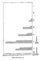
- the special behavior of the test boards in the hot tinning process, as described under le, is shown graphically in the drawing. There, the damaged portion of the surface (front and back) of individual boards is given in%.
- the surface damage relates primarily to solder residues in the form of beads, cobweb-like threads and nets.
- the dyes mentioned in Example 1 were added in the same amounts as there.
- the parts by weight of the polymers relate to 50% solutions in methoxybutanol (corresponding to the concentration given in Example 1a), the parts by weight of the other components to solvent-free solids.
- Example 11 to 24 The solids content of the mixtures in Examples 11 to 24 was analogous to Example 1 by adding methoxybutanol to a viscosity of 8.5 to 50 dPa ⁇ s brought. This is usually achieved, again in analogy to Example 1, with solids contents of 58 to 68%.
Landscapes
- Physics & Mathematics (AREA)
- Chemical & Material Sciences (AREA)
- General Physics & Mathematics (AREA)
- Chemical Kinetics & Catalysis (AREA)
- Medicinal Chemistry (AREA)
- Engineering & Computer Science (AREA)
- Health & Medical Sciences (AREA)
- Polymers & Plastics (AREA)
- Organic Chemistry (AREA)
- Spectroscopy & Molecular Physics (AREA)
- Manufacturing & Machinery (AREA)
- Microelectronics & Electronic Packaging (AREA)
- Non-Metallic Protective Coatings For Printed Circuits (AREA)
- Polymerisation Methods In General (AREA)
- Epoxy Resins (AREA)
- Macromonomer-Based Addition Polymer (AREA)
- Dental Preparations (AREA)
- Manufacturing Of Printed Circuit Boards (AREA)
- Preparing Plates And Mask In Photomechanical Process (AREA)
- Addition Polymer Or Copolymer, Post-Treatments, Or Chemical Modifications (AREA)
- Adhesives Or Adhesive Processes (AREA)
- Photosensitive Polymer And Photoresist Processing (AREA)
- Reinforced Plastic Materials (AREA)
- Analysing Materials By The Use Of Radiation (AREA)
Applications Claiming Priority (2)
| Application Number | Priority Date | Filing Date | Title |
|---|---|---|---|
| DE3931467A DE3931467A1 (de) | 1989-09-21 | 1989-09-21 | Durch strahlung polymerisierbares gemisch und verfahren zur herstellung einer loetstopmaske |
| DE3931467 | 1989-09-21 |
Publications (3)
| Publication Number | Publication Date |
|---|---|
| EP0418733A2 true EP0418733A2 (fr) | 1991-03-27 |
| EP0418733A3 EP0418733A3 (en) | 1992-03-04 |
| EP0418733B1 EP0418733B1 (fr) | 1998-01-14 |
Family
ID=6389856
Family Applications (1)
| Application Number | Title | Priority Date | Filing Date |
|---|---|---|---|
| EP90117636A Expired - Lifetime EP0418733B1 (fr) | 1989-09-21 | 1990-09-13 | Mélange polymérisable par radiation et procédé de préparation d'un masque pour soudage |
Country Status (15)
| Country | Link |
|---|---|
| US (2) | US5264324A (fr) |
| EP (1) | EP0418733B1 (fr) |
| JP (1) | JP2662083B2 (fr) |
| KR (1) | KR0161970B1 (fr) |
| AT (1) | ATE162316T1 (fr) |
| AU (1) | AU633363B2 (fr) |
| CA (1) | CA2025831C (fr) |
| DE (2) | DE3931467A1 (fr) |
| DK (1) | DK0418733T3 (fr) |
| ES (1) | ES2110956T3 (fr) |
| FI (1) | FI904605A7 (fr) |
| IE (1) | IE903402A1 (fr) |
| IL (1) | IL95739A (fr) |
| NO (1) | NO904115L (fr) |
| ZA (1) | ZA907479B (fr) |
Cited By (6)
| Publication number | Priority date | Publication date | Assignee | Title |
|---|---|---|---|---|
| EP0591759A3 (fr) * | 1992-10-09 | 1994-04-20 | Morton Int Inc | |
| EP0651601A1 (fr) * | 1993-10-28 | 1995-05-03 | Du Pont De Nemours (Deutschland) Gmbh | Mélange photopolymérisable et procédé de fabrication de masques de soudure |
| EP0549946A3 (fr) * | 1991-12-21 | 1995-05-10 | Hoechst Ag | |
| EP0573031A3 (fr) * | 1992-06-03 | 1995-06-14 | Nippon Paint Co Ltd | Procédé de fabrication des masques structurés pour soudage. |
| EP0625001A3 (fr) * | 1993-05-13 | 1995-11-02 | Morton Int Inc | Procédé de métallisation selon une image de plaques à circuit imprimé structurées. |
| EP0903636A3 (fr) * | 1997-09-18 | 2000-03-08 | E.I. Du Pont De Nemours And Company | Composition photosensible assistée thermiquement et méthode d'utilisation de cette composition dans la fabrication de lignes conductrices fines |
Families Citing this family (15)
| Publication number | Priority date | Publication date | Assignee | Title |
|---|---|---|---|---|
| JP2706858B2 (ja) * | 1991-07-30 | 1998-01-28 | 富士写真フイルム株式会社 | 光重合性組成物 |
| US5545510A (en) * | 1995-03-28 | 1996-08-13 | Mac Dermid, Inc. | Photodefinable dielectric composition useful in the manufacture of printed circuits |
| US5925499A (en) * | 1995-08-01 | 1999-07-20 | Morton International, Inc. | Epoxy-containing waterborne photoimageable composition |
| US5844308A (en) * | 1997-08-20 | 1998-12-01 | Cts Corporation | Integrated circuit anti-bridging leads design |
| US6645696B1 (en) * | 2001-11-30 | 2003-11-11 | Euv Llc. | Photoimageable composition |
| DE10204114A1 (de) * | 2002-02-01 | 2003-08-14 | Basf Coatings Ag | Thermisch und mit aktinischer Strahlung härtbares Stoffgemisch, Verfahren zu seiner Herstellung und seine Verwendung |
| CN1445248A (zh) * | 2002-02-15 | 2003-10-01 | 希普雷公司 | 官能化聚合物 |
| JP4500657B2 (ja) * | 2004-11-30 | 2010-07-14 | 旭化成イーマテリアルズ株式会社 | パターン形成材料、並びにパターン形成装置及びパターン形成方法 |
| JP2006208730A (ja) * | 2005-01-27 | 2006-08-10 | Fuji Photo Film Co Ltd | パターン形成材料、並びにパターン形成装置及びパターン形成方法 |
| JP5661293B2 (ja) * | 2010-02-08 | 2015-01-28 | 太陽ホールディングス株式会社 | 光硬化性樹脂組成物、ドライフィルム、硬化物及びプリント配線板 |
| JP5829035B2 (ja) * | 2011-03-31 | 2015-12-09 | 太陽インキ製造株式会社 | 光硬化性樹脂組成物、ドライフィルム、硬化物及びプリント配線板 |
| JPWO2012141153A1 (ja) * | 2011-04-13 | 2014-07-28 | 太陽インキ製造株式会社 | 光硬化性樹脂組成物、ドライフィルム、硬化物及びプリント配線板 |
| DE102011083791A1 (de) * | 2011-09-29 | 2013-04-04 | Robert Bosch Gmbh | Verfahren zur Herstellung einer Lötverbindung |
| TWI541594B (zh) * | 2011-09-30 | 2016-07-11 | 太陽油墨製造股份有限公司 | A photosensitive resin composition, a hardened film thereof, and a printed wiring board |
| JP2017165846A (ja) * | 2016-03-15 | 2017-09-21 | アーゼッド・エレクトロニック・マテリアルズ(ルクセンブルグ)ソシエテ・ア・レスポンサビリテ・リミテ | 微細パターン形成用組成物およびそれを用いた微細パターン形成方法 |
Family Cites Families (25)
| Publication number | Priority date | Publication date | Assignee | Title |
|---|---|---|---|---|
| DE2064080C3 (de) * | 1970-12-28 | 1983-11-03 | Hoechst Ag, 6230 Frankfurt | Lichtempfindliches Gemisch |
| US3887450A (en) * | 1971-02-04 | 1975-06-03 | Dynachem Corp | Photopolymerizable compositions containing polymeric binding agents |
| US3776729A (en) * | 1971-02-22 | 1973-12-04 | Ibm | Photosensitive dielectric composition and process of using the same |
| DE2363806B2 (de) * | 1973-12-21 | 1979-05-17 | Hoechst Ag, 6000 Frankfurt | Lichtempfindliches Gemisch |
| ZA757984B (en) * | 1974-10-04 | 1976-12-29 | Dynachem Corp | Polymers for aqueous processed photoresists |
| DE2861486D1 (en) * | 1977-11-21 | 1982-02-18 | Ciba Geigy Ag | Process for the application of soldering masks to printed circuits with through holes for contacting |
| US4278752A (en) * | 1978-09-07 | 1981-07-14 | E. I. Du Pont De Nemours And Company | Flame retardant radiation sensitive element |
| BR8001021A (pt) * | 1979-02-26 | 1980-10-29 | Du Pont | Material resistente de pelicula seca, rolo ajustado, mascara de solda e processo para a modificacao seletiva de uma superficie |
| US4390615A (en) * | 1979-11-05 | 1983-06-28 | Courtney Robert W | Coating compositions |
| DE3114931A1 (de) * | 1981-04-13 | 1982-10-28 | Hoechst Ag, 6000 Frankfurt | Durch strahlung polymerisierbares gemisch und daraus hergestelltes photopolymerisierbares kopiermaterial |
| DE3120052A1 (de) * | 1981-05-20 | 1982-12-09 | Hoechst Ag, 6000 Frankfurt | Durch strahlung polymerisierbares gemisch und damit hergestelltes kopiermaterial |
| DE3134123A1 (de) * | 1981-08-28 | 1983-03-17 | Hoechst Ag, 6000 Frankfurt | Durch strahlung polymerisierbares gemisch und daraushergestelltes photopolymerisierbares kopiermaterial |
| DE3265242D1 (en) * | 1981-09-17 | 1985-09-12 | Ciba Geigy Ag | Light-sensitive coating agent and its use in protection purposes |
| CA1194637A (fr) * | 1982-04-26 | 1985-10-01 | Charles R. Morgan | Compositions a teneur de matiere thermoplastique durcissables a l'ultraviolet ou a chaud |
| DE3236560A1 (de) * | 1982-10-02 | 1984-04-05 | Hoechst Ag, 6230 Frankfurt | Lichtempfindliches schichtuebertragungsmaterial und verfahren zur herstellung einer photoresistschablone |
| US4479983A (en) * | 1983-01-07 | 1984-10-30 | International Business Machines Corporation | Method and composition for applying coatings on printed circuit boards |
| DE3412992A1 (de) * | 1984-04-06 | 1985-10-24 | Hoechst Ag, 6230 Frankfurt | Durch strahlung polymerisierbares gemisch und verfahren zum aufbringen von markierungen auf eine loetstopresistschicht |
| JPH0618856B2 (ja) * | 1986-02-14 | 1994-03-16 | 日本合成ゴム株式会社 | 液状感光性樹脂組成物およびそれを用いる画像形成法 |
| JPS63258975A (ja) * | 1986-12-26 | 1988-10-26 | Toshiba Corp | ソルダーレジストインキ組成物 |
| JP2604173B2 (ja) * | 1987-02-25 | 1997-04-30 | 東京応化工業株式会社 | 耐熱性感光性樹脂組成物 |
| JP2604174B2 (ja) * | 1987-03-25 | 1997-04-30 | 東京応化工業株式会社 | 耐熱性感光性樹脂組成物 |
| JPH0717737B2 (ja) * | 1987-11-30 | 1995-03-01 | 太陽インキ製造株式会社 | 感光性熱硬化性樹脂組成物及びソルダーレジストパターン形成方法 |
| DE3853283T2 (de) * | 1987-12-07 | 1995-07-13 | Thiokol Morton Inc | Zusammensetzungen für aufzeichnungsmaterialien. |
| JPH0748108B2 (ja) * | 1988-02-02 | 1995-05-24 | イビデン株式会社 | 感光性樹脂組成物 |
| JPH01203424A (ja) * | 1988-02-09 | 1989-08-16 | Toagosei Chem Ind Co Ltd | 硬化性組成物 |
-
1989
- 1989-09-21 DE DE3931467A patent/DE3931467A1/de not_active Withdrawn
-
1990
- 1990-09-13 DK DK90117636T patent/DK0418733T3/da active
- 1990-09-13 DE DE59010796T patent/DE59010796D1/de not_active Expired - Fee Related
- 1990-09-13 AT AT90117636T patent/ATE162316T1/de not_active IP Right Cessation
- 1990-09-13 ES ES90117636T patent/ES2110956T3/es not_active Expired - Lifetime
- 1990-09-13 EP EP90117636A patent/EP0418733B1/fr not_active Expired - Lifetime
- 1990-09-19 ZA ZA907479A patent/ZA907479B/xx unknown
- 1990-09-19 FI FI904605A patent/FI904605A7/fi not_active Application Discontinuation
- 1990-09-19 IL IL9573990A patent/IL95739A/en not_active IP Right Cessation
- 1990-09-19 KR KR1019900014795A patent/KR0161970B1/ko not_active Expired - Fee Related
- 1990-09-20 NO NO90904115A patent/NO904115L/no unknown
- 1990-09-20 CA CA002025831A patent/CA2025831C/fr not_active Expired - Fee Related
- 1990-09-20 JP JP25168090A patent/JP2662083B2/ja not_active Expired - Fee Related
- 1990-09-20 IE IE340290A patent/IE903402A1/en not_active IP Right Cessation
- 1990-09-20 US US07/585,642 patent/US5264324A/en not_active Expired - Lifetime
- 1990-09-20 AU AU63047/90A patent/AU633363B2/en not_active Ceased
-
1993
- 1993-10-27 US US08/144,115 patent/US5387486A/en not_active Expired - Lifetime
Cited By (6)
| Publication number | Priority date | Publication date | Assignee | Title |
|---|---|---|---|---|
| EP0549946A3 (fr) * | 1991-12-21 | 1995-05-10 | Hoechst Ag | |
| EP0573031A3 (fr) * | 1992-06-03 | 1995-06-14 | Nippon Paint Co Ltd | Procédé de fabrication des masques structurés pour soudage. |
| EP0591759A3 (fr) * | 1992-10-09 | 1994-04-20 | Morton Int Inc | |
| EP0625001A3 (fr) * | 1993-05-13 | 1995-11-02 | Morton Int Inc | Procédé de métallisation selon une image de plaques à circuit imprimé structurées. |
| EP0651601A1 (fr) * | 1993-10-28 | 1995-05-03 | Du Pont De Nemours (Deutschland) Gmbh | Mélange photopolymérisable et procédé de fabrication de masques de soudure |
| EP0903636A3 (fr) * | 1997-09-18 | 2000-03-08 | E.I. Du Pont De Nemours And Company | Composition photosensible assistée thermiquement et méthode d'utilisation de cette composition dans la fabrication de lignes conductrices fines |
Also Published As
| Publication number | Publication date |
|---|---|
| JP2662083B2 (ja) | 1997-10-08 |
| EP0418733B1 (fr) | 1998-01-14 |
| IL95739A0 (en) | 1991-06-30 |
| IL95739A (en) | 1995-03-15 |
| NO904115D0 (no) | 1990-09-20 |
| DK0418733T3 (da) | 1998-09-07 |
| ATE162316T1 (de) | 1998-01-15 |
| KR0161970B1 (ko) | 1999-01-15 |
| NO904115L (no) | 1991-03-22 |
| JPH03164742A (ja) | 1991-07-16 |
| AU6304790A (en) | 1991-03-28 |
| US5387486A (en) | 1995-02-07 |
| ZA907479B (en) | 1991-06-26 |
| FI904605A7 (fi) | 1991-03-22 |
| KR910006781A (ko) | 1991-04-30 |
| FI904605A0 (fi) | 1990-09-19 |
| IE903402A1 (en) | 1991-04-10 |
| US5264324A (en) | 1993-11-23 |
| AU633363B2 (en) | 1993-01-28 |
| DE3931467A1 (de) | 1991-04-04 |
| DE59010796D1 (de) | 1998-02-19 |
| EP0418733A3 (en) | 1992-03-04 |
| CA2025831C (fr) | 2001-11-20 |
| CA2025831A1 (fr) | 1991-03-22 |
| ES2110956T3 (es) | 1998-03-01 |
Similar Documents
| Publication | Publication Date | Title |
|---|---|---|
| EP0418733B1 (fr) | Mélange polymérisable par radiation et procédé de préparation d'un masque pour soudage | |
| DE3613107C2 (fr) | ||
| EP0075537B1 (fr) | Procédé de revêtement de circuits imprimés | |
| DE3885260T2 (de) | Lichtempfindliche wärmehärtbare Harzzusammensetzung und Methode zur Herstellung von Lötstoppmasken damit. | |
| EP0493317B1 (fr) | Composition radiosensible à base de l'eau comme solvant ou dispersant respectivement | |
| DE3715412C2 (fr) | ||
| EP0063304B1 (fr) | Composition polymérisable par radiation et matériau à copier photopolymérisable préparé à partir de celle-ci | |
| EP0134574B1 (fr) | Mélange durcissable photosensible pour la réalisation de matériau d'enregistrement à effet positif | |
| DE19622464A1 (de) | Licht- und wärmehärtbare Zusammensetzung, die mit einer wässerigen Alkalilösung entwickelbar ist | |
| EP0633503A1 (fr) | Compositions photopolymérisables | |
| EP0141389A2 (fr) | Procédé pour la fabrication de réserves structurées selon une image et réserve à sec pour ce procédé | |
| EP0549946A2 (fr) | Mélange polymérisable par irradiation et procédé de préparation d'un masque pour soudure | |
| DE69630555T2 (de) | Photostrukturierbare dielektrische Zusammensetzung zur Verwendung in der Herstellung von Leiterplatten | |
| DE3887367T2 (de) | Wärmebeständige, lichtempfindliche Harzzusammensetzung. | |
| DE4419874A1 (de) | Alkalilösliches Harz und Harzzusammensetzung | |
| DE69019067T2 (de) | Lichtempfindliche Bildaufzeichnungszusammensetzungen. | |
| DE3704067A1 (de) | Verfahren zum nicht-klebrigmachen der oberflaeche einer harzplatte | |
| EP0011786B1 (fr) | Composition photopolymérisable | |
| EP0141921A1 (fr) | Mélange photopolymérisable et matériel pour l'enregistrement fabriqué à partir de ce mélange | |
| DE3930586A1 (de) | Photodruckfaehige, permanente abdeckmasken | |
| EP0651601B1 (fr) | Mélange photopolymérisable et procédé de fabrication de masques de soudure | |
| EP0021429A2 (fr) | Matériel de copie photopolymérisable et procédé de préparation d'images en relief | |
| DE69300657T2 (de) | Foto- und wärmehärtende Beschichtungszusammensetzung und Verfahren zum Herstellen von Resist-Lötmasken. | |
| EP0591759A2 (fr) | Mélange polymérisable par radiation et procédé de préparation d'un masque pour soudure | |
| DE60017524T2 (de) | Ein flexibles Oligomer enthaltende, lichtempfindliche Zusammensetzung |
Legal Events
| Date | Code | Title | Description |
|---|---|---|---|
| PUAI | Public reference made under article 153(3) epc to a published international application that has entered the european phase |
Free format text: ORIGINAL CODE: 0009012 |
|
| AK | Designated contracting states |
Kind code of ref document: A2 Designated state(s): AT BE CH DE DK ES FR GB IT LI NL SE |
|
| RIN1 | Information on inventor provided before grant (corrected) |
Inventor name: DECKER, RUDOLF Inventor name: ERBES, KURT Inventor name: HERWIG, WALTER, DR. Inventor name: EMMELIUS, MICHAEL, DR. |
|
| PUAL | Search report despatched |
Free format text: ORIGINAL CODE: 0009013 |
|
| AK | Designated contracting states |
Kind code of ref document: A3 Designated state(s): AT BE CH DE DK ES FR GB IT LI NL SE |
|
| 17P | Request for examination filed |
Effective date: 19920627 |
|
| RAP1 | Party data changed (applicant data changed or rights of an application transferred) |
Owner name: MORTON INTERNATIONAL, INC. |
|
| 17Q | First examination report despatched |
Effective date: 19960214 |
|
| GRAG | Despatch of communication of intention to grant |
Free format text: ORIGINAL CODE: EPIDOS AGRA |
|
| GRAH | Despatch of communication of intention to grant a patent |
Free format text: ORIGINAL CODE: EPIDOS IGRA |
|
| GRAH | Despatch of communication of intention to grant a patent |
Free format text: ORIGINAL CODE: EPIDOS IGRA |
|
| RAP1 | Party data changed (applicant data changed or rights of an application transferred) |
Owner name: MORTON INTERNATIONAL, INC. |
|
| GRAA | (expected) grant |
Free format text: ORIGINAL CODE: 0009210 |
|
| AK | Designated contracting states |
Kind code of ref document: B1 Designated state(s): AT BE CH DE DK ES FR GB IT LI NL SE |
|
| REF | Corresponds to: |
Ref document number: 162316 Country of ref document: AT Date of ref document: 19980115 Kind code of ref document: T |
|
| REG | Reference to a national code |
Ref country code: CH Ref legal event code: NV Representative=s name: KIRKER & CIE SA Ref country code: CH Ref legal event code: EP |
|
| ITF | It: translation for a ep patent filed | ||
| GBT | Gb: translation of ep patent filed (gb section 77(6)(a)/1977) |
Effective date: 19980116 |
|
| REF | Corresponds to: |
Ref document number: 59010796 Country of ref document: DE Date of ref document: 19980219 |
|
| REG | Reference to a national code |
Ref country code: ES Ref legal event code: FG2A Ref document number: 2110956 Country of ref document: ES Kind code of ref document: T3 |
|
| ET | Fr: translation filed | ||
| REG | Reference to a national code |
Ref country code: DK Ref legal event code: T3 |
|
| PLBE | No opposition filed within time limit |
Free format text: ORIGINAL CODE: 0009261 |
|
| STAA | Information on the status of an ep patent application or granted ep patent |
Free format text: STATUS: NO OPPOSITION FILED WITHIN TIME LIMIT |
|
| 26N | No opposition filed | ||
| REG | Reference to a national code |
Ref country code: GB Ref legal event code: IF02 |
|
| PGFP | Annual fee paid to national office [announced via postgrant information from national office to epo] |
Ref country code: NL Payment date: 20040816 Year of fee payment: 15 |
|
| PGFP | Annual fee paid to national office [announced via postgrant information from national office to epo] |
Ref country code: AT Payment date: 20040819 Year of fee payment: 15 |
|
| PGFP | Annual fee paid to national office [announced via postgrant information from national office to epo] |
Ref country code: GB Payment date: 20040908 Year of fee payment: 15 |
|
| PGFP | Annual fee paid to national office [announced via postgrant information from national office to epo] |
Ref country code: FR Payment date: 20040920 Year of fee payment: 15 |
|
| PGFP | Annual fee paid to national office [announced via postgrant information from national office to epo] |
Ref country code: SE Payment date: 20040921 Year of fee payment: 15 |
|
| PGFP | Annual fee paid to national office [announced via postgrant information from national office to epo] |
Ref country code: DK Payment date: 20040924 Year of fee payment: 15 Ref country code: CH Payment date: 20040924 Year of fee payment: 15 |
|
| PGFP | Annual fee paid to national office [announced via postgrant information from national office to epo] |
Ref country code: ES Payment date: 20041008 Year of fee payment: 15 |
|
| PGFP | Annual fee paid to national office [announced via postgrant information from national office to epo] |
Ref country code: BE Payment date: 20041021 Year of fee payment: 15 |
|
| PGFP | Annual fee paid to national office [announced via postgrant information from national office to epo] |
Ref country code: DE Payment date: 20041102 Year of fee payment: 15 |
|
| PG25 | Lapsed in a contracting state [announced via postgrant information from national office to epo] |
Ref country code: IT Free format text: LAPSE BECAUSE OF NON-PAYMENT OF DUE FEES;WARNING: LAPSES OF ITALIAN PATENTS WITH EFFECTIVE DATE BEFORE 2007 MAY HAVE OCCURRED AT ANY TIME BEFORE 2007. THE CORRECT EFFECTIVE DATE MAY BE DIFFERENT FROM THE ONE RECORDED. Effective date: 20050913 Ref country code: GB Free format text: LAPSE BECAUSE OF NON-PAYMENT OF DUE FEES Effective date: 20050913 Ref country code: AT Free format text: LAPSE BECAUSE OF NON-PAYMENT OF DUE FEES Effective date: 20050913 |
|
| PG25 | Lapsed in a contracting state [announced via postgrant information from national office to epo] |
Ref country code: SE Free format text: LAPSE BECAUSE OF NON-PAYMENT OF DUE FEES Effective date: 20050914 Ref country code: ES Free format text: LAPSE BECAUSE OF NON-PAYMENT OF DUE FEES Effective date: 20050914 |
|
| PG25 | Lapsed in a contracting state [announced via postgrant information from national office to epo] |
Ref country code: LI Free format text: LAPSE BECAUSE OF NON-PAYMENT OF DUE FEES Effective date: 20050930 Ref country code: DK Free format text: LAPSE BECAUSE OF NON-PAYMENT OF DUE FEES Effective date: 20050930 Ref country code: CH Free format text: LAPSE BECAUSE OF NON-PAYMENT OF DUE FEES Effective date: 20050930 Ref country code: BE Free format text: LAPSE BECAUSE OF NON-PAYMENT OF DUE FEES Effective date: 20050930 |
|
| NLS | Nl: assignments of ep-patents |
Owner name: ROHM AND HAAS CHEMICALS LLC Effective date: 20050914 |
|
| PG25 | Lapsed in a contracting state [announced via postgrant information from national office to epo] |
Ref country code: NL Free format text: LAPSE BECAUSE OF NON-PAYMENT OF DUE FEES Effective date: 20060401 Ref country code: DE Free format text: LAPSE BECAUSE OF NON-PAYMENT OF DUE FEES Effective date: 20060401 |
|
| REG | Reference to a national code |
Ref country code: DK Ref legal event code: EBP |
|
| REG | Reference to a national code |
Ref country code: CH Ref legal event code: PL |
|
| EUG | Se: european patent has lapsed | ||
| GBPC | Gb: european patent ceased through non-payment of renewal fee |
Effective date: 20050913 |
|
| PG25 | Lapsed in a contracting state [announced via postgrant information from national office to epo] |
Ref country code: FR Free format text: LAPSE BECAUSE OF NON-PAYMENT OF DUE FEES Effective date: 20060531 |
|
| NLV4 | Nl: lapsed or anulled due to non-payment of the annual fee |
Effective date: 20060401 |
|
| REG | Reference to a national code |
Ref country code: FR Ref legal event code: ST Effective date: 20060531 |
|
| REG | Reference to a national code |
Ref country code: ES Ref legal event code: FD2A Effective date: 20050914 |
|
| BERE | Be: lapsed |
Owner name: *MORTON INTERNATIONAL INC. Effective date: 20050930 |