EP0431444A2 - Méthode de fabrication d'un transistor MIS ayant une électrode de porte à type de conductivité accordé - Google Patents
Méthode de fabrication d'un transistor MIS ayant une électrode de porte à type de conductivité accordé Download PDFInfo
- Publication number
- EP0431444A2 EP0431444A2 EP90122648A EP90122648A EP0431444A2 EP 0431444 A2 EP0431444 A2 EP 0431444A2 EP 90122648 A EP90122648 A EP 90122648A EP 90122648 A EP90122648 A EP 90122648A EP 0431444 A2 EP0431444 A2 EP 0431444A2
- Authority
- EP
- European Patent Office
- Prior art keywords
- gate electrode
- impurity
- source
- conductivity type
- substrate
- Prior art date
- Legal status (The legal status is an assumption and is not a legal conclusion. Google has not performed a legal analysis and makes no representation as to the accuracy of the status listed.)
- Withdrawn
Links
Images


Classifications
-
- H—ELECTRICITY
- H10—SEMICONDUCTOR DEVICES; ELECTRIC SOLID-STATE DEVICES NOT OTHERWISE PROVIDED FOR
- H10D—INORGANIC ELECTRIC SEMICONDUCTOR DEVICES
- H10D30/00—Field-effect transistors [FET]
- H10D30/01—Manufacture or treatment
- H10D30/021—Manufacture or treatment of FETs having insulated gates [IGFET]
- H10D30/0223—Manufacture or treatment of FETs having insulated gates [IGFET] having source and drain regions or source and drain extensions self-aligned to sides of the gate
-
- H—ELECTRICITY
- H10—SEMICONDUCTOR DEVICES; ELECTRIC SOLID-STATE DEVICES NOT OTHERWISE PROVIDED FOR
- H10D—INORGANIC ELECTRIC SEMICONDUCTOR DEVICES
- H10D30/00—Field-effect transistors [FET]
- H10D30/60—Insulated-gate field-effect transistors [IGFET]
-
- H—ELECTRICITY
- H10—SEMICONDUCTOR DEVICES; ELECTRIC SOLID-STATE DEVICES NOT OTHERWISE PROVIDED FOR
- H10P—GENERIC PROCESSES OR APPARATUS FOR THE MANUFACTURE OR TREATMENT OF DEVICES COVERED BY CLASS H10
- H10P32/00—Diffusion of dopants within, into or out of wafers, substrates or parts of devices
- H10P32/10—Diffusion of dopants within, into or out of semiconductor bodies or layers
- H10P32/14—Diffusion of dopants within, into or out of semiconductor bodies or layers within a single semiconductor body or layer in a solid phase; between different semiconductor bodies or layers, both in a solid phase
- H10P32/1408—Diffusion of dopants within, into or out of semiconductor bodies or layers within a single semiconductor body or layer in a solid phase; between different semiconductor bodies or layers, both in a solid phase from or through or into an external applied layer, e.g. photoresist or nitride layers
-
- H—ELECTRICITY
- H10—SEMICONDUCTOR DEVICES; ELECTRIC SOLID-STATE DEVICES NOT OTHERWISE PROVIDED FOR
- H10P—GENERIC PROCESSES OR APPARATUS FOR THE MANUFACTURE OR TREATMENT OF DEVICES COVERED BY CLASS H10
- H10P32/00—Diffusion of dopants within, into or out of wafers, substrates or parts of devices
- H10P32/10—Diffusion of dopants within, into or out of semiconductor bodies or layers
- H10P32/17—Diffusion of dopants within, into or out of semiconductor bodies or layers characterised by the semiconductor material
- H10P32/171—Diffusion of dopants within, into or out of semiconductor bodies or layers characterised by the semiconductor material being group IV material
-
- H—ELECTRICITY
- H10—SEMICONDUCTOR DEVICES; ELECTRIC SOLID-STATE DEVICES NOT OTHERWISE PROVIDED FOR
- H10P—GENERIC PROCESSES OR APPARATUS FOR THE MANUFACTURE OR TREATMENT OF DEVICES COVERED BY CLASS H10
- H10P32/00—Diffusion of dopants within, into or out of wafers, substrates or parts of devices
- H10P32/30—Diffusion for doping of conductive or resistive layers
- H10P32/302—Doping polycrystalline silicon or amorphous silicon layers
Definitions
- the present invention relates to the method of producing an MIS transistor having a gate electrode of the same conductivity type as that of source and drain regions of the transistor.
- gate electrode is referred to as "matched conductivity type”.
- ion implantation method or predeposition method is utilized to dope the same conductivity type of impurity into the gate electrode and the source and drain regions.
- the conventional doping methods have various drawbacks.
- the impurity particles are implanted into a certain depth due to kinetic energy of accelerated impurity ion particles. Therefore, when activation of the ion particles is carried out by thermal treatment after the ion implantation, the impurity particles are diffused from the gate electrode to a gate insulating film and further to a channel region.
- impurity particles may be diffused from the gate electrode into the channel region similarly as in case of the ion implantation.
- the impurity particles having one conductivity type opposite to that of the channel region are inadvertently diffused from the gate electrode into the channel region disposed under the gate electrode, thereby causing drawbacks such as shift of threshold voltage of the transistor, and reduction of carrier mobility due to excess density of impurity atoms in the channel region.
- drawbacks are most serious in the P channel MIS transistor having the matched conductivity type of gate electrode which contains P type impurity of boron (B) which has relatively great diffusion coefficient.
- an object of the present invention is to provide a new method of doping an impurity limitatively only into a shallow surface portion of the matched conductivity type gate electrode so as to avoid diffusion of the impurity into the channel region.
- an active surface is exposed on a surface of a gate electrode and on a patterned surface area of a semiconductor layer. Then, a gas containing an impurity component is applied to the exposed active surface to deposit thereon an adsorption film containing the impurity component. Thereafter, thermal treatment is effected to diffuse the impurity component concurrently into the gate electrode and into the patterned surface area to form a pair of source and drain regions in the semiconductor layer by solid-phase diffusion.
- MLD Molecular Layer Doping
- Figs. lA - lD are a step diagram showing the inventive method of producing an MIS transistor having a gate electrode of the matched conductivity type
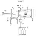
- Fig. 2 is a block diagram showing an impurity doping apparatus
- Figs. 3A - 3D are a step diagram showing a variation of the inventive method.
- Fig. 4 is a diagram showing an impurity distribution in a channel region under the gate electrode.
- Figs. lA - lD are a step diagram showing a typical method of producing an MIS transistor having a gate electrode of the matched conductivity type according to the invention.
- This embodiment is directed to the production of a P channel transistor in which a P type impurity, for example boron, is doped into a device region.
- a semiconductor substrate l composed of silicon.
- a field oxide film 2 is formed on a surface of the substrate l to define a device isolation region.
- the field oxide film 2 is formed by selective thermal oxidation treatment to surround a device region.
- a gate insulating film 3 and a gate electrode 4 are formed in the device region.
- the gate insulating film 3 is composed of silicon oxide layer, silicon nitride layer or a double layer of silicon oxide film and silicon nitride film.
- the gate electrode 4 is composed of polysilicon which is deposited by, for example, chemical vapor deposition and then patterned in a predetermined shape.
- the original gate insulating film 3 is partly etched away through a mask of the patterned gate electrode 4 concurrently at the patterning of the gate electrode 4 or after the patterning so as to form a window portion.
- the thus prepared device region is covered with a natural oxide film 5.
- activation treatment or cleaning treatment is applied to a surface of the device region to remove the natural oxide film 5.
- hydrogen gas(H2) is introduced for five minutes into a vacuum chamber held at less than l x l0 ⁇ 4 Pa of the background pressure while heating the substrate l at 850°C in the chamber, so that the chamber pressure is raised to l.3 ⁇ l0 ⁇ 2 Pa. Consequently, an active surface is exposed on the gate electrode 4 and on the window portion of the semiconductor layer not covered by the gate insulating film 3 within the device region.
- diborane gas(B2H6) 9 is introduced at l ⁇ l0 ⁇ 3 Pa for l00 seconds while heating the substrate l at 825°C so as to deposit an impurity adsorption film 6 on the exposed active surface over the gate electrode and the window portion of the semiconductor substrate.
- the impurity adsorption film 6 contains boron atoms produced by thermal dissociation of the diborane gas 9.
- annealing is effected such that the impurity boron contained in the adsorption film 6 is diffused into the gate electrode 4 by solid-phase diffusion to optimumly set electroconductance of the gate electrode 4.
- the impurity boron is diffused into the substrate l through the window portion to form source region 7 and drain region 8, which contain significant amount of the P type impurity of boron.
- the diffusion density and diffusion depth of the source region 7 and drain region 8 may depend on the amount of impurity boron contained in the adsorption film 6 and on the annealing condition.
- the amount of impurity boron can be controlled quite accurately by regulating charging pressure and charging time interval of the diborane gas 9 and the substrate temperature during the charging of the diborane gas.
- the impurity components are distributed at relatively high concentration in the surface or outer portion of the gate electrode and at relatively low concentration in the inner portion of the gate electrode. Therefore, the amount of impurity diffused from the gate electrode 4 into the channel region through the gate insulating film 3 can be reduced.
- the impurity doping apparatus is comprised of a vacuum chamber l2 made of quartz, in which is placed centrally a silicon substrate l.
- a heating unit l3 is provided to controllably heat the substrate l to set a desired substrate temperature by an infrared lamp heating or resistance heating.
- the interior of vacuum chamber l2 can be evacuated in high vacuum degree by a high vacuum evacuation system l4 comprised of plural pumps including a main vacuum pump composed of a turbo molecular pump.
- a pressure gage l5 is utilized to continuously monitor the vacuum degree of the chamber l2.
- a transportation mechanism l8 is utilized to transport the silicon substrate l to the chamber l2 from a load chamber l7 through a gate valve l6a which is held open during the transportation.
- the load chamber l7 is normally evacuated by another evacuation system ll while a gate valve l6b is held open except during the supply of substrates to the load chamber l7 and during the transportation of each substrate from the load chamber l7.
- a gas supply source l9 is connected to the vacuum chamber l2 through a gas flow control system 20.
- the gas supply source l9 contains a plurality of bottles for storing various gas species needed to carry out the inventive impurity doping.
- the gas flow control system 20 is operated to control gas species, gas charging time and gas charging pressure.
- activation treatment or cleaning treatment is applied to a surface of the gate electrode and a surface of a device region not covered by an gate insulating film.
- the silicon substrate l is placed in a center of the vacuum chamber l2 held at less than l ⁇ l0 ⁇ 4 Pa of the background pressure.
- hydrogen gas is introduced into the chamber l2 from the gas supply source l9 while maintaining a temperature of the substrate l at, for example, 850°C.
- the hydrogen gas is filled in the chamber l2 for a predetermined time interval at the condition of l.3 x l0 ⁇ 2 Pa of the chamber pressure.
- an inert film i.e., natural oxide film is removed from the gate electrode surface and from the surface of device region not covered by the gate insulating film, thereby exposing a chemically active silicon surface.
- This activation treatment is important for preparation of the following adsorption treatment. Namely, the adsorption film is selectively deposited only on the active silicon surface.
- the adsorption treatment is carried out by charging a source gas into the chamber l2.
- the substrate l is heated at a temperature in the range from 400°C to 900°C.
- the source gas is composed of a gaseous compound containing an impurity component of P or N type.
- diborane gas(B2H6) containing P type impurity component of boron is introduced into the chamber to form the adsorption film containing boron.
- the substrate l is annealed for a predetermined time interval to effect diffusion of the impurity boron from a diffusion source of the adsorption film 6.
- the diffused impurity of boron is activated concurrently.
- the impurity components are directly deposited on the active surface of the semiconductor material without an intermediate oxide film. Therefore, the impurity dose can be accurately controlled as compared to the conventional predeposition. Since the impurity is diffused internally by annealing treatment after adsorbing the impurity on the active surface, a quite shallow junction can be formed as compared to the conventional ion implantation by which an impurity particle is initially injected in a certain depth.
- Figs. 3A - 3D are a step diagram showing a variation of the inventive method of producing the MIS transistor.
- a semiconductor substrate l composed of silicon.
- a field oxide film 2 is formed on a surface of the substrate l.
- a gate insulating film 3 and a gate electrode 4 are formed in a device region.
- a side wall l0 is formed around the gate electrode 4.
- the side wall l0 is provided by anisotropic etching a thick silicon oxide film deposited on the patterned gate electrode 4 by CVD.
- the side wall l0 has a thickness smaller than an expected value of horizontal diffusion span.
- the thick oxide film is removed by dry etching or wet etching from a top surface of the gate electrode 4 and from a window portion extending between the side wall l0 and the field oxide film 2.
- a thin natural oxide film 5 may be formed on the top surface of the gate electrode 4 and on the window portion immediately after removing the thick oxide film.
- the natural oxide film 5 is removed by activation treatment in manner similar to the Fig. lB step of the previous embodiment. Consequently, a silicon active surface is exposed on the top surface of the gate electrode 4 and on the window portion existing between the edge of the gate insulating film 3 or side wall l0 and the edge of the field oxide film 2.
- a diborane gas 9 is introduced in manner similar to the Fig. lC step of the previous embodiment. Consequently, an impurity adsorption film 6 is deposited on the top surface of the gate electrode 4 which is not covered by the side wall l0 and on the exposed window portion.
- annealing treatment is carried out so that the impurity boron contained in the impurity adsorption film 6 is diffused into the gate electrode 4 by solid-phase diffusion to optimumly set electric conductance of the gate electrode.
- the impurity is diffused into the window portion to form a source region 7 and a drain region 8, having significant amount of the P type dopants.
- the source region 7 and the drain region 8 are formed such that their PN junction portions extends under the gate electrode 4 in order to avoid offset.
- annealing temperature and time is optimumly set so that the impurity atoms diffuse horizontally from the impurity adsorption film 6 through a diffusion distance which exceeds the thickness of the side wall l0.
- the substrate l is annealed at 850°C for thirty minutes so that the diffusion region extends horizontally by about 0.l ⁇ m.
- the gate electrode 4 has the same conductivity type as that of the source region 7 and drain region 8. Since the gate electrode 4 is surrounded by the side wall l0 along its side edge, the impurity adsorption film 6 is deposited only on the top surface of the gate electrode. Accordingly, after annealing treatment for diffusion and activation of the impurity atoms, the impurity atoms are distributed at relatively high concentration in the upper section of the gate electrode 4 and at relatively low concentration in the lower section thereof in the vicinity of the gate insulating film 3. Therefore, the amount of the diffused impurities is further reduced, as compared to the previous embodiment, from the gate electrode to the cannel region.
- the diborane gas is utilized to dope a P type impurity into a silicon layer.
- III-group elements such as trimethyl gallium (THG) and boron trichloride (BCl3).
- TMG trimethyl gallium
- BCl3 boron trichloride
- N type impurity to the silicon layer is effected by various gas compound species of V-group elements, such as arsine(AsH3), phosphorus trichloride(PCl3), antimony pentachloride(SbCl5) and phosphine(PH3).
- a typical substrate temperature is set for the cleaning treatment, adsorption treatment and diffusion treatment in the above described embodiments.
- the substrate temperature may be optimumly set in the range from 800°C to l200°C for the surface cleaning or activation treatment in conjunction with the level of background pressure and ambient gas species.
- the cleaning treatment can be effected by other ways such as application of HF gas or irradiation of ultraviolet ray, effective to remove a natural oxide film.
- the substrate temperature is generally set optimumly in the range from 400°C to 950°C for the adsorption treatment.
- the substrate temperature for the diffusion treatment may be preferably set in the range comparable to that of the adsorption treatment.
- Annealing after the adsorption of the impurity can be effected by rapid thermal annealing using IR rump, laser beam annealing or plasma annealing so as to form further shallow diffusion depth in the source region 7 and the drain region 8.
- the gate electrode and the pair of source and drain regions are concurrently doped with the same conductivity type of impurity.
- the doped impurity atoms are distributed at relatively high concentration in the upper section of the gate electrode and at relatively low concentration in the vicinity of the gate insulating film in contrast to the conventional ion implantation and predeposition technology, thereby efficiently suppressing undesired diffusion of the impurity from the gate electrode into the channel region as shown in the Fig. 4 graph. Therefore, the inventive method can effectively avoid shift of transistor threshold voltage and avoid reduction of the carrier mobility due to increase of the impurity in the channel region.
Landscapes
- Insulated Gate Type Field-Effect Transistor (AREA)
Applications Claiming Priority (2)
| Application Number | Priority Date | Filing Date | Title |
|---|---|---|---|
| JP1318560A JP2920546B2 (ja) | 1989-12-06 | 1989-12-06 | 同極ゲートmisトランジスタの製造方法 |
| JP318560/89 | 1989-12-06 |
Publications (2)
| Publication Number | Publication Date |
|---|---|
| EP0431444A2 true EP0431444A2 (fr) | 1991-06-12 |
| EP0431444A3 EP0431444A3 (en) | 1992-03-18 |
Family
ID=18100496
Family Applications (1)
| Application Number | Title | Priority Date | Filing Date |
|---|---|---|---|
| EP19900122648 Withdrawn EP0431444A3 (en) | 1989-12-06 | 1990-11-27 | Method of producing mis transistor having gate electrode of matched conductivity type |
Country Status (4)
| Country | Link |
|---|---|
| US (1) | US5874352A (fr) |
| EP (1) | EP0431444A3 (fr) |
| JP (1) | JP2920546B2 (fr) |
| CA (1) | CA2031417A1 (fr) |
Families Citing this family (5)
| Publication number | Priority date | Publication date | Assignee | Title |
|---|---|---|---|---|
| US6673673B1 (en) * | 1997-04-22 | 2004-01-06 | Samsung Electronics Co., Ltd. | Method for manufacturing a semiconductor device having hemispherical grains |
| JP2002184710A (ja) * | 2000-12-18 | 2002-06-28 | Sony Corp | 半導体層のドーピング方法、薄膜半導体素子の製造方法、及び薄膜半導体素子 |
| JP4090225B2 (ja) * | 2001-08-29 | 2008-05-28 | 東京エレクトロン株式会社 | 半導体装置の製造方法、及び、基板処理方法 |
| JP2007266265A (ja) * | 2006-03-28 | 2007-10-11 | Toshiba Corp | 不純物拡散方法及び半導体装置の製造方法 |
| KR101057188B1 (ko) * | 2008-11-11 | 2011-08-16 | 주식회사 하이닉스반도체 | Pmos 트랜지스터의 제조방법 및 이를 이용한 반도체 소자의 듀얼 게이트 형성방법 |
Family Cites Families (30)
| Publication number | Priority date | Publication date | Assignee | Title |
|---|---|---|---|---|
| GB1133422A (en) * | 1967-01-19 | 1968-11-13 | Marconi Co Ltd | Improvements in or relating to methods of manufacturing planar transistors |
| US3590471A (en) * | 1969-02-04 | 1971-07-06 | Bell Telephone Labor Inc | Fabrication of insulated gate field-effect transistors involving ion implantation |
| US3673679A (en) * | 1970-12-01 | 1972-07-04 | Texas Instruments Inc | Complementary insulated gate field effect devices |
| JPS5145951B2 (fr) * | 1972-06-07 | 1976-12-06 | ||
| DE2245852C3 (de) * | 1972-09-19 | 1979-03-29 | Siemens Ag, 1000 Berlin Und 8000 Muenchen | Verfahren zur Herstellung mehrerer dotierter Halbleiterbereiche |
| US3888706A (en) * | 1973-08-06 | 1975-06-10 | Rca Corp | Method of making a compact guard-banded mos integrated circuit device using framelike diffusion-masking structure |
| US4242691A (en) * | 1978-09-18 | 1980-12-30 | Mitsubishi Denki Kabushiki Kaisha | MOS Semiconductor device |
| JPS5674921A (en) * | 1979-11-22 | 1981-06-20 | Toshiba Corp | Manufacturing method of semiconductor and apparatus thereof |
| US4335537A (en) * | 1979-11-28 | 1982-06-22 | Plectrum Pty. Limited | Toy aircraft |
| US4345366A (en) * | 1980-10-20 | 1982-08-24 | Ncr Corporation | Self-aligned all-n+ polysilicon CMOS process |
| JPS57149770A (en) * | 1981-03-11 | 1982-09-16 | Mitsubishi Electric Corp | Manufacture of semiconductor device |
| US4618381A (en) * | 1983-05-26 | 1986-10-21 | Fuji Electric Corporate Research And Development Ltd. | Method for adding impurities to semiconductor base material |
| JPS61292358A (ja) * | 1985-06-19 | 1986-12-23 | Fujitsu Ltd | Mis型電界効果トランジスタの製造方法 |
| JPH0831602B2 (ja) * | 1986-06-30 | 1996-03-27 | 沖電気工業株式会社 | Mis型電界効果トランジスタの製造方法 |
| US4791074A (en) * | 1986-08-29 | 1988-12-13 | Kabushiki Kaisha Toshiba | Method of manufacturing a semiconductor apparatus |
| JPH07120635B2 (ja) * | 1986-12-26 | 1995-12-20 | 株式会社東芝 | 半導体装置の製造方法 |
| JPS63239939A (ja) * | 1987-03-27 | 1988-10-05 | Toshiba Corp | 半導体基体内への不純物導入方法及び装置 |
| JPS62271475A (ja) * | 1987-04-03 | 1987-11-25 | Hitachi Ltd | 半導体装置 |
| US4912065A (en) * | 1987-05-28 | 1990-03-27 | Matsushita Electric Industrial Co., Ltd. | Plasma doping method |
| US4861729A (en) * | 1987-08-24 | 1989-08-29 | Matsushita Electric Industrial Co., Ltd. | Method of doping impurities into sidewall of trench by use of plasma source |
| JPH01125935A (ja) * | 1987-11-11 | 1989-05-18 | Seiko Instr & Electron Ltd | 半導体装置の製造方法 |
| KR910009030B1 (ko) * | 1987-12-30 | 1991-10-28 | 후지쓰 가부시끼가이샤 | 얇은 접합의 형성방법 및 상기 얇은 접합을 갖는 반도체장치 |
| US5183777A (en) * | 1987-12-30 | 1993-02-02 | Fujitsu Limited | Method of forming shallow junctions |
| JPH01192159A (ja) * | 1988-01-27 | 1989-08-02 | Mitsubishi Electric Corp | 半導体装置 |
| EP0413982B1 (fr) * | 1989-07-27 | 1997-05-14 | Junichi Nishizawa | Méthode de dopage à l'aide d'une source de diffusion adsorbée |
| EP0417457A3 (en) * | 1989-08-11 | 1991-07-03 | Seiko Instruments Inc. | Method of producing field effect transistor |
| CA2031254A1 (fr) * | 1989-12-01 | 1991-06-02 | Kenji Aoki | Methode de dopage des barrieres dans les dispositifs a semiconducteur |
| JP3079575B2 (ja) * | 1990-12-20 | 2000-08-21 | 株式会社日立製作所 | 半導体装置の製造方法 |
| US5242859A (en) * | 1992-07-14 | 1993-09-07 | International Business Machines Corporation | Highly doped semiconductor material and method of fabrication thereof |
| US5599735A (en) * | 1994-08-01 | 1997-02-04 | Texas Instruments Incorporated | Method for doped shallow junction formation using direct gas-phase doping |
-
1989
- 1989-12-06 JP JP1318560A patent/JP2920546B2/ja not_active Expired - Lifetime
-
1990
- 1990-11-27 EP EP19900122648 patent/EP0431444A3/en not_active Withdrawn
- 1990-12-04 CA CA002031417A patent/CA2031417A1/fr not_active Abandoned
-
1995
- 1995-10-18 US US08/544,454 patent/US5874352A/en not_active Expired - Lifetime
Also Published As
| Publication number | Publication date |
|---|---|
| CA2031417A1 (fr) | 1991-06-07 |
| US5874352A (en) | 1999-02-23 |
| EP0431444A3 (en) | 1992-03-18 |
| JPH03178134A (ja) | 1991-08-02 |
| JP2920546B2 (ja) | 1999-07-19 |
Similar Documents
| Publication | Publication Date | Title |
|---|---|---|
| US5925574A (en) | Method of producing a bipolar transistor | |
| US5366922A (en) | Method for producing CMOS transistor | |
| US5124272A (en) | Method of producing field effect transistor | |
| US5338697A (en) | Doping method of barrier region in semiconductor device | |
| JP2928930B2 (ja) | 不純物ドーピング装置 | |
| US5256162A (en) | Apparatus for forming shallow electrical junctions | |
| EP0430167A2 (fr) | Méthode de fabrication d'un dispositif à jonction PN | |
| JPS63166220A (ja) | 半導体装置の製造方法 | |
| EP0430168A2 (fr) | Méthode de dopage des bords d'une tranchée d'un semi-conducteur | |
| EP0431444A2 (fr) | Méthode de fabrication d'un transistor MIS ayant une électrode de porte à type de conductivité accordé | |
| US5851909A (en) | Method of producing semiconductor device using an adsorption layer | |
| EP0430166A2 (fr) | Méthode pour doper des films semi-conducteurs et ruban semi-conducteur configuré | |
| JP3578345B2 (ja) | 半導体装置の製造方法および半導体装置 | |
| US5532185A (en) | Impurity doping method with adsorbed diffusion source | |
| JP3263058B2 (ja) | 半導体内壁に対する不純物の注入方法 | |
| JP2928929B2 (ja) | 不純物ドーピング方法 | |
| EP0431616A2 (fr) | Méthode de fabrication d'un transistor CMOS | |
| JP2926344B2 (ja) | 電界効果トランジスタの製造方法 | |
| JP2926419B2 (ja) | 半導体装置の製造方法 | |
| JP3023481B2 (ja) | 半導体膜に対する不純物の注入方法 | |
| JP2973011B2 (ja) | 半導体素子分離領域の形成方法 | |
| JPH03218638A (ja) | 半導体装置の製造方法 | |
| KR19990027876A (ko) | 불순물 확산영역 형성방법 | |
| JPH02249275A (ja) | 半導体装置の製造方法 | |
| JPH02202065A (ja) | 静電誘導型トランジスタの製造方法 |
Legal Events
| Date | Code | Title | Description |
|---|---|---|---|
| PUAI | Public reference made under article 153(3) epc to a published international application that has entered the european phase |
Free format text: ORIGINAL CODE: 0009012 |
|
| AK | Designated contracting states |
Kind code of ref document: A2 Designated state(s): DE FR GB |
|
| PUAL | Search report despatched |
Free format text: ORIGINAL CODE: 0009013 |
|
| AK | Designated contracting states |
Kind code of ref document: A3 Designated state(s): DE FR GB |
|
| 17P | Request for examination filed |
Effective date: 19920914 |
|
| 17Q | First examination report despatched |
Effective date: 19940830 |
|
| STAA | Information on the status of an ep patent application or granted ep patent |
Free format text: STATUS: THE APPLICATION IS DEEMED TO BE WITHDRAWN |
|
| 18D | Application deemed to be withdrawn |
Effective date: 19950929 |