EP0442414B1 - Substrat composé à semi-conducteur et procédé pour sa fabrication - Google Patents
Substrat composé à semi-conducteur et procédé pour sa fabrication Download PDFInfo
- Publication number
- EP0442414B1 EP0442414B1 EP91101865A EP91101865A EP0442414B1 EP 0442414 B1 EP0442414 B1 EP 0442414B1 EP 91101865 A EP91101865 A EP 91101865A EP 91101865 A EP91101865 A EP 91101865A EP 0442414 B1 EP0442414 B1 EP 0442414B1
- Authority
- EP
- European Patent Office
- Prior art keywords
- compound semiconductor
- gaas
- crystal layer
- semi
- crystal
- Prior art date
- Legal status (The legal status is an assumption and is not a legal conclusion. Google has not performed a legal analysis and makes no representation as to the accuracy of the status listed.)
- Expired - Lifetime
Links
Images


Classifications
-
- H—ELECTRICITY
- H10—SEMICONDUCTOR DEVICES; ELECTRIC SOLID-STATE DEVICES NOT OTHERWISE PROVIDED FOR
- H10D—INORGANIC ELECTRIC SEMICONDUCTOR DEVICES
- H10D62/00—Semiconductor bodies, or regions thereof, of devices having potential barriers
- H10D62/10—Shapes, relative sizes or dispositions of the regions of the semiconductor bodies; Shapes of the semiconductor bodies
- H10D62/17—Semiconductor regions connected to electrodes not carrying current to be rectified, amplified or switched, e.g. channel regions
-
- H—ELECTRICITY
- H10—SEMICONDUCTOR DEVICES; ELECTRIC SOLID-STATE DEVICES NOT OTHERWISE PROVIDED FOR
- H10P—GENERIC PROCESSES OR APPARATUS FOR THE MANUFACTURE OR TREATMENT OF DEVICES COVERED BY CLASS H10
- H10P14/00—Formation of materials, e.g. in the shape of layers or pillars
- H10P14/20—Formation of materials, e.g. in the shape of layers or pillars of semiconductor materials
- H10P14/29—Formation of materials, e.g. in the shape of layers or pillars of semiconductor materials characterised by the substrates
- H10P14/2901—Materials
- H10P14/2907—Materials being Group IIIA-VA materials
- H10P14/2911—Arsenides
-
- H—ELECTRICITY
- H10—SEMICONDUCTOR DEVICES; ELECTRIC SOLID-STATE DEVICES NOT OTHERWISE PROVIDED FOR
- H10P—GENERIC PROCESSES OR APPARATUS FOR THE MANUFACTURE OR TREATMENT OF DEVICES COVERED BY CLASS H10
- H10P14/00—Formation of materials, e.g. in the shape of layers or pillars
- H10P14/20—Formation of materials, e.g. in the shape of layers or pillars of semiconductor materials
- H10P14/34—Deposited materials, e.g. layers
- H10P14/3402—Deposited materials, e.g. layers characterised by the chemical composition
- H10P14/3414—Deposited materials, e.g. layers characterised by the chemical composition being group IIIA-VIA materials
- H10P14/3418—Phosphides
-
- H—ELECTRICITY
- H10—SEMICONDUCTOR DEVICES; ELECTRIC SOLID-STATE DEVICES NOT OTHERWISE PROVIDED FOR
- H10P—GENERIC PROCESSES OR APPARATUS FOR THE MANUFACTURE OR TREATMENT OF DEVICES COVERED BY CLASS H10
- H10P14/00—Formation of materials, e.g. in the shape of layers or pillars
- H10P14/20—Formation of materials, e.g. in the shape of layers or pillars of semiconductor materials
- H10P14/34—Deposited materials, e.g. layers
- H10P14/3402—Deposited materials, e.g. layers characterised by the chemical composition
- H10P14/3414—Deposited materials, e.g. layers characterised by the chemical composition being group IIIA-VIA materials
- H10P14/3421—Arsenides
Definitions
- the present invention relates to a method of manufacturing a compound semiconductor device.
- GaAs is known well as a type of a compound semiconductor.
- the GaAs is made to have a resistivity of 106 ⁇ cm or more, it has semi-insulating characteristics.
- active elements are formed in a semi-insulating GaAs substrate, they are not advantageously required to be electrically isolated from each other using a field insulating film.
- a semi-insulating GaAs single-crystal is conventionally made using a single-crystal manufacturing technique such as an LEC method, and the single-crystal is sliced to manufacture semi-insulating GaAs substrates.
- the semi-insulating GaAs single-crystal is constituted by bonding two types of atoms, a shearing stress acting inside the Gas single-crystal is stronger than that of a silicon single-crystal, and a dislocation density in the GaAs single-crystal is disadvantageously increased.
- the present invention has been made in consideration of the above problem, and has as its object to provide a method of manufacturing a compound semiconductor device with a substrate having a low dislocation density.
- the above object can be achieved by the following arrangement.
- a dislocation density can be decreased.
- a high-resistance single-crystal layer having a low dislocation density i.e., a single-crystal layer having semi-insulating characteristics can be formed.
- the high-resistance single-crystal layer is formed in a portion where an active element is to be formed, a compound semiconductor substrate having a low dislocation density and even advantageously having a high-resistance, i.e., semi-insulating characteristics can be obtained.
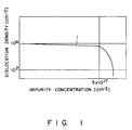
- a curve I in Fig. 1 indicates a decrease in dislocation density when an impurity is doped in GaAs after a crystal is grown. The decrease in dislocation density typically occurs when an n-type impurity is doped.
- a doping concentration of the impurity at a time when the dislocation density is rapidly decreased is 5 ⁇ 1017 cm ⁇ 3 or more. This phenomenon is not limited to the GaAs, and it occurs in a compound semiconductor such as GaP or InP consisting of two elements.
- n-type impurity Silicon or carbon is used as an n-type impurity, and selenium, magnesium or the like is used as a p-type impurity.
- a doping concentration is set to be 5 ⁇ 1017 cm ⁇ 3 or more to obtain a compound semiconductor single-crystal having a low dislocation density.
- the present invention is made on the basis of the above phenomenon, n-type GaAs in which a single-crystal, e.g., a silicon element, having a density of 5 ⁇ 1017 cm-3 or more is doped as an impurity is grown by an LEC method or an HB method, thereby forming an n-type GaAs single-crystal 10 having a low dislocation density (Fig. 2A).
- the single-crystal 10 is cut (Fig. 2B).
- the cut single-crystal 10 is sliced to obtain an n-type GaAs base 12 (Fig. 2C).
- the base 12 sliced as described above is prospectively used as a substrate for epitaxial growth.
- a high-resistance GaAs single-crystal layer 14 having a resistivity of 106 ⁇ cm is epitaxially grown on the surface of the base 12 (Fig. 2E).
- an amount of impurity contained in GaAs is decreased, or the GaAs is undoped.
- the high-resistance GaAs single-crystal layer 14 is prospectively used as a portion where an active element is to be formed.
- a compound semiconductor substrate 16 according to the present invention is finished by the above method.
- a dislocation density of a single-crystal layer which is epitaxially grown is generally lower than that of a substrate on which the single-crystal layer is grown.
- the dislocation density of the n-type GaAs base 12 is decreased by doping an impurity, and the dislocation density of the GaAs single-crystal layer 14 grown on the base 12 is further decreased.
- a dislocation density is about 50,000 cm ⁇ at a portion where an active element is to be formed.
- the dislocation density of the GaAs single-crystal layer 14 where an active element is to be formed can be set to be 100 cm ⁇ or less.
- Fig. 3 is a partially enlarged sectional view showing the GaAs substrate 16 shown in Fig. 2E
- Fig. 4 is a sectional view showing a condition wherein an active element is formed on the GaAs substrate 16.
- the GaAs single-crystal layer 14 which is undoped to have a high-resistance is stacked on the n-type GaAs base 12 by epitaxial growth.
- the high-resistance GaAs single-crystal layer 14 is a layer where an active element 18 is prospectively formed, and an active region 20 prospectively serving as a source, a drain, and a channel of the active element 18 is formed on the single-crystal layer 14.
- the high-resistance GaAs single-crystal layer 14 is formed to have a resistivity of 106 ⁇ cm or more, a field insulating film for isolating the active elements 18 from each other need not be formed (the high-resistance GaAs single-crystal layer 14 has semi-insulating characteristics).
- the high-resistance GaAs single-crystal layer 14 is epitaxially grown on the n-type GaAs base 12 having a low dislocation density, the dislocation density of the single-crystal layer 14 is also low.
- the active elements 18 formed on the GaAs single-crystal layer 14 having a low dislocation density have excellent characteristics, and variations in characteristics of all the active elements 18 can be decreased.
- the variations in characteristics of the active elements 18 can be decreased, in all cases wherein an IC/LSI is formed and wherein an individual semiconductor device is formed, the performance of the IC/LSI and the individual semiconductor device can be improved, and a yield of the products can be improved.
- a thickness t of the high-resistance GaAs single-crystal layer 14 is required to be a minimum thickness required for forming the active region 20.
- the thickness t of the high-resistance GaAs single-crystal layer 14 is set to be about 500 nm or more, it can sufficiently cope with formation of the active region 20.
- a method of growing a crystal at an atomic layer level such as MBE, MOCVD, or MOMBE is preferably used from the viewpoint of improvements of a film quality and controllability of the film thickness t .
- the base 12 contains an impurity to have a low dislocation density.
- the single-crystal layer 14 stacked thereon is undoped to have a high resistance so as to have semi-insulating characteristics.
- an impurity having an effect of decreasing the dislocation density of the base 12 carbon, selenium, magnesium, or the like is used in addition to silicon.
- the dislocation density of the single-crystal can be decreased.
Landscapes
- Recrystallisation Techniques (AREA)
- Physical Deposition Of Substances That Are Components Of Semiconductor Devices (AREA)
- Element Separation (AREA)
Claims (9)
- Procédé de fabrication d'un dispositif à semiconducteur composite, incluant un substrat semiconducteur composite (16), comprenant l'étape de croissance épitaxiale du même semiconducteur composite en tant que base semiconductrice composite (12) afin de former une couche monocristalline épitaxiale semi-isolante (14) présentant une résistance suffisamment élevée pour assurer des caractéristiques semi-isolantes pour l'isolation électrique d'éléments actifs (18) sur le substrat, la couche étant formée sur une surface principale de ladite base semiconductrice composite contenant une impureté selon une concentration suffisamment élevée pour assurer une densité de dislocations significativement diminuée ; et l'étape de formation d'éléments actifs dans ladite couche épitaxiale semi-isolante, ladite couche épitaxiale semi-isolante étant utilisée en tant que région d'isolation d'éléments pour isoler lesdits éléments actifs les uns des autres.
- Procédé selon la revendication 1, caractérisé en ce qu'une concentration d'une impureté de ladite base semiconductrice composite n'est pas inférieure à 5 x 10¹⁷ cm⁻³.
- Procédé selon la revendication 1, caractérisé en ce qu'une résistivité de ladite couche monocristalline à résistance élevée n'est pas inférieure à 10⁶ Ω·cm.
- Procédé selon la revendication 1, caractérisé en ce que ladite couche monocristalline à résistance élevée est une couche non dopée.
- Procédé selon la revendication 1, caractérisé en ce que ladite couche monocristalline à résistance élevée présente une épaisseur non inférieure à 500 nm.
- Procédé selon la revendication 1, caractérisé en ce que ladite impureté est un élément choisi parmi le groupe comprenant le silicium, le sélénium et le magnésium.
- Procédé selon la revendication 1, caractérisé en ce que ledit semiconducteur composite comprend un élément pris dans le groupe III, IV ou V.
- Procédé selon la revendication 7, caractérisé en ce que ledit semiconducteur composite est choisi parmi le groupe comprenant le GaAs, le GaP et l'InP.
- Procédé selon la revendication 1, caractérisé en ce que l'étape de croissance épitaxiale du même semiconducteur composite que ladite base semiconductrice composite comprend l'étape de réalisation d'un procédé choisi parmi le groupe comprenant un procédé d'épitaxie par jet moléculaire (MBE), un procédé de dépôt chimique en phase vapeur d'organo-métallique (MOCVD) et un procédé d'épitaxie par jet moléculaire d'organo-métallique (MOMBE).
Applications Claiming Priority (2)
| Application Number | Priority Date | Filing Date | Title |
|---|---|---|---|
| JP2032697A JPH0831409B2 (ja) | 1990-02-14 | 1990-02-14 | 化合物半導体装置およびその製造方法 |
| JP32697/90 | 1990-02-14 |
Publications (3)
| Publication Number | Publication Date |
|---|---|
| EP0442414A2 EP0442414A2 (fr) | 1991-08-21 |
| EP0442414A3 EP0442414A3 (en) | 1991-10-23 |
| EP0442414B1 true EP0442414B1 (fr) | 1996-04-24 |
Family
ID=12366045
Family Applications (1)
| Application Number | Title | Priority Date | Filing Date |
|---|---|---|---|
| EP91101865A Expired - Lifetime EP0442414B1 (fr) | 1990-02-14 | 1991-02-11 | Substrat composé à semi-conducteur et procédé pour sa fabrication |
Country Status (5)
| Country | Link |
|---|---|
| US (1) | US5599389A (fr) |
| EP (1) | EP0442414B1 (fr) |
| JP (1) | JPH0831409B2 (fr) |
| KR (1) | KR910016060A (fr) |
| DE (1) | DE69118941T2 (fr) |
Families Citing this family (22)
| Publication number | Priority date | Publication date | Assignee | Title |
|---|---|---|---|---|
| JP3171807B2 (ja) * | 1997-01-24 | 2001-06-04 | 東京エレクトロン株式会社 | 洗浄装置及び洗浄方法 |
| US6815790B2 (en) * | 2003-01-10 | 2004-11-09 | Rapiscan, Inc. | Position sensing detector for the detection of light within two dimensions |
| US7057254B2 (en) * | 2003-05-05 | 2006-06-06 | Udt Sensors, Inc. | Front illuminated back side contact thin wafer detectors |
| US8120023B2 (en) | 2006-06-05 | 2012-02-21 | Udt Sensors, Inc. | Low crosstalk, front-side illuminated, back-side contact photodiode array |
| US7242069B2 (en) * | 2003-05-05 | 2007-07-10 | Udt Sensors, Inc. | Thin wafer detectors with improved radiation damage and crosstalk characteristics |
| US7576369B2 (en) * | 2005-10-25 | 2009-08-18 | Udt Sensors, Inc. | Deep diffused thin photodiodes |
| US7256470B2 (en) * | 2005-03-16 | 2007-08-14 | Udt Sensors, Inc. | Photodiode with controlled current leakage |
| US8519503B2 (en) * | 2006-06-05 | 2013-08-27 | Osi Optoelectronics, Inc. | High speed backside illuminated, front side contact photodiode array |
| US8035183B2 (en) * | 2003-05-05 | 2011-10-11 | Udt Sensors, Inc. | Photodiodes with PN junction on both front and back sides |
| US8164151B2 (en) * | 2007-05-07 | 2012-04-24 | Osi Optoelectronics, Inc. | Thin active layer fishbone photodiode and method of manufacturing the same |
| US7880258B2 (en) * | 2003-05-05 | 2011-02-01 | Udt Sensors, Inc. | Thin wafer detectors with improved radiation damage and crosstalk characteristics |
| US7709921B2 (en) | 2008-08-27 | 2010-05-04 | Udt Sensors, Inc. | Photodiode and photodiode array with improved performance characteristics |
| US7279731B1 (en) | 2006-05-15 | 2007-10-09 | Udt Sensors, Inc. | Edge illuminated photodiodes |
| US8686529B2 (en) | 2010-01-19 | 2014-04-01 | Osi Optoelectronics, Inc. | Wavelength sensitive sensor photodiodes |
| US7656001B2 (en) * | 2006-11-01 | 2010-02-02 | Udt Sensors, Inc. | Front-side illuminated, back-side contact double-sided PN-junction photodiode arrays |
| US7655999B2 (en) * | 2006-09-15 | 2010-02-02 | Udt Sensors, Inc. | High density photodiodes |
| US8766392B2 (en) * | 2007-05-07 | 2014-07-01 | Osi Optoelectronics, Inc. | Thin active layer fishbone photodiode with a shallow N+ layer and method of manufacturing the same |
| US9178092B2 (en) | 2006-11-01 | 2015-11-03 | Osi Optoelectronics, Inc. | Front-side illuminated, back-side contact double-sided PN-junction photodiode arrays |
| US20100053802A1 (en) * | 2008-08-27 | 2010-03-04 | Masaki Yamashita | Low Power Disk-Drive Motor Driver |
| CN102292477B (zh) * | 2009-01-20 | 2015-11-25 | 住友电气工业株式会社 | 导电GaAs的晶体和衬底及它们的形成方法 |
| US8399909B2 (en) * | 2009-05-12 | 2013-03-19 | Osi Optoelectronics, Inc. | Tetra-lateral position sensing detector |
| US8912615B2 (en) | 2013-01-24 | 2014-12-16 | Osi Optoelectronics, Inc. | Shallow junction photodiode for detecting short wavelength light |
Family Cites Families (14)
| Publication number | Priority date | Publication date | Assignee | Title |
|---|---|---|---|---|
| JPS53110973A (en) * | 1977-03-10 | 1978-09-28 | Futaba Denshi Kogyo Kk | Method and apparatus for manufacturing compounds |
| JPS54106169A (en) * | 1978-02-08 | 1979-08-20 | Nec Corp | Vapor epitaxial growth device |
| GB2030551B (en) * | 1978-09-22 | 1982-08-04 | Philips Electronic Associated | Growing a gaas layer doped with s se or te |
| JPS5591816A (en) * | 1978-12-29 | 1980-07-11 | Fujitsu Ltd | Manufacturing of semiconductor device |
| JPS5627972A (en) * | 1979-08-17 | 1981-03-18 | Oki Electric Ind Co Ltd | Manufacture of compound semiconductor device |
| JPS59184570A (ja) * | 1983-04-01 | 1984-10-19 | Matsushita Electric Ind Co Ltd | 電界効果トランジスタ |
| US4632710A (en) * | 1983-05-10 | 1986-12-30 | Raytheon Company | Vapor phase epitaxial growth of carbon doped layers of Group III-V materials |
| GB2156579B (en) * | 1984-03-15 | 1987-05-07 | Standard Telephones Cables Ltd | Field effect transistors |
| JPS613465A (ja) * | 1984-06-18 | 1986-01-09 | Fujitsu Ltd | 半導体装置及びその製造方法 |
| DE3682959D1 (de) * | 1985-06-21 | 1992-01-30 | Matsushita Electric Industrial Co Ltd | Bipolarer transistor mit heterouebergang und verfahren zu seiner herstellung. |
| JPH0670973B2 (ja) * | 1985-09-18 | 1994-09-07 | 住友電気工業株式会社 | 化合物半導体のエピタキシヤルウエハ |
| JP2504782B2 (ja) * | 1987-09-25 | 1996-06-05 | 住友電気工業株式会社 | 電界効果トランジスタの製造方法 |
| JPH01179411A (ja) * | 1988-01-08 | 1989-07-17 | Nec Corp | 3−5族化合物半導体気相成長方法 |
| US4935381A (en) * | 1988-12-09 | 1990-06-19 | The Aerospace Corporation | Process for growing GaAs epitaxial layers |
-
1990
- 1990-02-14 JP JP2032697A patent/JPH0831409B2/ja not_active Expired - Fee Related
-
1991
- 1991-02-07 KR KR1019910002056A patent/KR910016060A/ko not_active Ceased
- 1991-02-11 DE DE69118941T patent/DE69118941T2/de not_active Expired - Fee Related
- 1991-02-11 EP EP91101865A patent/EP0442414B1/fr not_active Expired - Lifetime
-
1994
- 1994-11-14 US US08/340,478 patent/US5599389A/en not_active Expired - Fee Related
Also Published As
| Publication number | Publication date |
|---|---|
| EP0442414A3 (en) | 1991-10-23 |
| DE69118941T2 (de) | 1996-09-26 |
| KR910016060A (ko) | 1991-09-30 |
| JPH0831409B2 (ja) | 1996-03-27 |
| US5599389A (en) | 1997-02-04 |
| EP0442414A2 (fr) | 1991-08-21 |
| DE69118941D1 (de) | 1996-05-30 |
| JPH03236218A (ja) | 1991-10-22 |
Similar Documents
| Publication | Publication Date | Title |
|---|---|---|
| EP0447327B1 (fr) | Dispositif semi-conducteur à hétérostructure | |
| US5599389A (en) | Compound semiconductor and method of manufacturing the same | |
| EP0097772B1 (fr) | Structure comportant un substrat monocristallin portant une couche de matériau semi-conducteur pour un dispositif | |
| US5311055A (en) | Trenched bipolar transistor structures | |
| US5256550A (en) | Fabricating a semiconductor device with strained Si1-x Gex layer | |
| EP0331467B1 (fr) | Méthode pour former une couche mince semi-conductrice | |
| US10825912B2 (en) | Integrated epitaxial metal electrodes | |
| JPH0766366A (ja) | 半導体積層構造体およびそれを用いた半導体装置 | |
| JPH08213331A (ja) | 転位欠陥の少ない半導体製造方法 | |
| US4837178A (en) | Method for producing a semiconductor integrated circuit having an improved isolation structure | |
| US5696034A (en) | Method for producing semiconductor substrate | |
| US10418457B2 (en) | Metal electrode with tunable work functions | |
| US4939102A (en) | Method of growing III-V semiconductor layers with high effective hole concentration | |
| EP0327122B1 (fr) | Dispositif semi-conducteur complémentaire bipolaire | |
| CN215527756U (zh) | 用于制备InSb功能层的衬底结构 | |
| EP3915133B1 (fr) | Électrodes métalliques épitaxiales intégrées | |
| US6036769A (en) | Preparation of semiconductor substrates | |
| JP3227083B2 (ja) | バイポーラトランジスタの作製方法 | |
| EP0460937B1 (fr) | Méthode pour la fabrication d'un laser à semi-conducteur | |
| EP0767969A1 (fr) | Preparation de substrats semi-conducteurs | |
| US5341006A (en) | Semiconductor device having diffusion-preventing layer between III-V layer and IV layer | |
| TW201115625A (en) | Method for making a semiconductor substrate, and semiconductor substrate | |
| JP2828980B2 (ja) | 半導体結晶の製造方法 | |
| JP5483558B2 (ja) | 半導体薄膜の形成方法 | |
| JPH04199507A (ja) | 3―V族化合物半導体へのn型不純物固相拡散方法 |
Legal Events
| Date | Code | Title | Description |
|---|---|---|---|
| PUAI | Public reference made under article 153(3) epc to a published international application that has entered the european phase |
Free format text: ORIGINAL CODE: 0009012 |
|
| 17P | Request for examination filed |
Effective date: 19910211 |
|
| AK | Designated contracting states |
Kind code of ref document: A2 Designated state(s): DE FR GB |
|
| PUAL | Search report despatched |
Free format text: ORIGINAL CODE: 0009013 |
|
| RHK1 | Main classification (correction) |
Ipc: C30B 29/40 |
|
| AK | Designated contracting states |
Kind code of ref document: A3 Designated state(s): DE FR GB |
|
| 17Q | First examination report despatched |
Effective date: 19940202 |
|
| GRAA | (expected) grant |
Free format text: ORIGINAL CODE: 0009210 |
|
| AK | Designated contracting states |
Kind code of ref document: B1 Designated state(s): DE FR GB |
|
| REF | Corresponds to: |
Ref document number: 69118941 Country of ref document: DE Date of ref document: 19960530 |
|
| ET | Fr: translation filed | ||
| GRAH | Despatch of communication of intention to grant a patent |
Free format text: ORIGINAL CODE: EPIDOS IGRA |
|
| PLBE | No opposition filed within time limit |
Free format text: ORIGINAL CODE: 0009261 |
|
| STAA | Information on the status of an ep patent application or granted ep patent |
Free format text: STATUS: NO OPPOSITION FILED WITHIN TIME LIMIT |
|
| 26N | No opposition filed | ||
| REG | Reference to a national code |
Ref country code: GB Ref legal event code: 746 Effective date: 19981007 |
|
| REG | Reference to a national code |
Ref country code: FR Ref legal event code: D6 |
|
| REG | Reference to a national code |
Ref country code: GB Ref legal event code: IF02 |
|
| PGFP | Annual fee paid to national office [announced via postgrant information from national office to epo] |
Ref country code: GB Payment date: 20060208 Year of fee payment: 16 |
|
| PGFP | Annual fee paid to national office [announced via postgrant information from national office to epo] |
Ref country code: DE Payment date: 20060209 Year of fee payment: 16 |
|
| PGFP | Annual fee paid to national office [announced via postgrant information from national office to epo] |
Ref country code: FR Payment date: 20060220 Year of fee payment: 16 |
|
| GBPC | Gb: european patent ceased through non-payment of renewal fee |
Effective date: 20070211 |
|
| REG | Reference to a national code |
Ref country code: FR Ref legal event code: ST Effective date: 20071030 |
|
| PG25 | Lapsed in a contracting state [announced via postgrant information from national office to epo] |
Ref country code: DE Free format text: LAPSE BECAUSE OF NON-PAYMENT OF DUE FEES Effective date: 20070901 |
|
| PG25 | Lapsed in a contracting state [announced via postgrant information from national office to epo] |
Ref country code: GB Free format text: LAPSE BECAUSE OF NON-PAYMENT OF DUE FEES Effective date: 20070211 Ref country code: FR Free format text: LAPSE BECAUSE OF NON-PAYMENT OF DUE FEES Effective date: 20070228 |