EP0450595A1 - Composé cristal liquide et dispositif d'affichage à cristaux liquides - Google Patents
Composé cristal liquide et dispositif d'affichage à cristaux liquides Download PDFInfo
- Publication number
- EP0450595A1 EP0450595A1 EP91105252A EP91105252A EP0450595A1 EP 0450595 A1 EP0450595 A1 EP 0450595A1 EP 91105252 A EP91105252 A EP 91105252A EP 91105252 A EP91105252 A EP 91105252A EP 0450595 A1 EP0450595 A1 EP 0450595A1
- Authority
- EP
- European Patent Office
- Prior art keywords
- compound
- liquid crystal
- phase
- antiferroelectric
- preparation
- Prior art date
- Legal status (The legal status is an assumption and is not a legal conclusion. Google has not performed a legal analysis and makes no representation as to the accuracy of the status listed.)
- Granted
Links
- 150000001875 compounds Chemical class 0.000 title claims abstract description 167
- 239000004973 liquid crystal related substance Substances 0.000 title claims abstract description 73
- 238000002360 preparation method Methods 0.000 description 34
- YXFVVABEGXRONW-UHFFFAOYSA-N Toluene Chemical compound CC1=CC=CC=C1 YXFVVABEGXRONW-UHFFFAOYSA-N 0.000 description 27
- 238000000034 method Methods 0.000 description 25
- FYSNRJHAOHDILO-UHFFFAOYSA-N thionyl chloride Chemical compound ClS(Cl)=O FYSNRJHAOHDILO-UHFFFAOYSA-N 0.000 description 24
- HEDRZPFGACZZDS-UHFFFAOYSA-N Chloroform Chemical compound ClC(Cl)Cl HEDRZPFGACZZDS-UHFFFAOYSA-N 0.000 description 20
- 230000004044 response Effects 0.000 description 20
- CSNNHWWHGAXBCP-UHFFFAOYSA-L Magnesium sulfate Chemical compound [Mg+2].[O-][S+2]([O-])([O-])[O-] CSNNHWWHGAXBCP-UHFFFAOYSA-L 0.000 description 18
- HEMHJVSKTPXQMS-UHFFFAOYSA-M Sodium hydroxide Chemical compound [OH-].[Na+] HEMHJVSKTPXQMS-UHFFFAOYSA-M 0.000 description 18
- LFQSCWFLJHTTHZ-UHFFFAOYSA-N Ethanol Chemical compound CCO LFQSCWFLJHTTHZ-UHFFFAOYSA-N 0.000 description 14
- 230000003287 optical effect Effects 0.000 description 14
- 230000007704 transition Effects 0.000 description 14
- 238000006243 chemical reaction Methods 0.000 description 13
- 239000000203 mixture Substances 0.000 description 13
- ILYSAKHOYBPSPC-UHFFFAOYSA-N 2-phenylbenzoic acid Chemical compound OC(=O)C1=CC=CC=C1C1=CC=CC=C1 ILYSAKHOYBPSPC-UHFFFAOYSA-N 0.000 description 12
- JUJWROOIHBZHMG-UHFFFAOYSA-N Pyridine Chemical compound C1=CC=NC=C1 JUJWROOIHBZHMG-UHFFFAOYSA-N 0.000 description 12
- XLYOFNOQVPJJNP-UHFFFAOYSA-N water Substances O XLYOFNOQVPJJNP-UHFFFAOYSA-N 0.000 description 12
- VEXZGXHMUGYJMC-UHFFFAOYSA-N Hydrochloric acid Chemical compound Cl VEXZGXHMUGYJMC-UHFFFAOYSA-N 0.000 description 11
- 238000005259 measurement Methods 0.000 description 11
- 239000004990 Smectic liquid crystal Substances 0.000 description 10
- 238000010992 reflux Methods 0.000 description 10
- 239000002904 solvent Substances 0.000 description 10
- VMKOFRJSULQZRM-UHFFFAOYSA-N 1-bromooctane Chemical compound CCCCCCCCBr VMKOFRJSULQZRM-UHFFFAOYSA-N 0.000 description 9
- 229910052943 magnesium sulfate Inorganic materials 0.000 description 9
- 235000019341 magnesium sulphate Nutrition 0.000 description 9
- 0 **c1ccc(*c(cc2)ccc2-c2ccc(*3*C3)cc2)cc1 Chemical compound **c1ccc(*c(cc2)ccc2-c2ccc(*3*C3)cc2)cc1 0.000 description 8
- 238000002834 transmittance Methods 0.000 description 8
- LSXKDWGTSHCFPP-UHFFFAOYSA-N 1-bromoheptane Chemical compound CCCCCCCBr LSXKDWGTSHCFPP-UHFFFAOYSA-N 0.000 description 7
- YGTCFEJZVJXZIT-UHFFFAOYSA-N C1=CC(OCCCCCCCCCCCC)=CC=C1C1=CCC(C=2C(=CC=CC=2)C(=O)OC(C)CCC)(C(O)=O)C=C1 Chemical compound C1=CC(OCCCCCCCCCCCC)=CC=C1C1=CCC(C=2C(=CC=CC=2)C(=O)OC(C)CCC)(C(O)=O)C=C1 YGTCFEJZVJXZIT-UHFFFAOYSA-N 0.000 description 7
- 238000000862 absorption spectrum Methods 0.000 description 7
- 125000000217 alkyl group Chemical group 0.000 description 7
- 230000000052 comparative effect Effects 0.000 description 7
- 239000007864 aqueous solution Substances 0.000 description 6
- WGQKYBSKWIADBV-UHFFFAOYSA-N benzylamine Chemical compound NCC1=CC=CC=C1 WGQKYBSKWIADBV-UHFFFAOYSA-N 0.000 description 6
- 238000002955 isolation Methods 0.000 description 6
- 239000012044 organic layer Substances 0.000 description 6
- UMJSCPRVCHMLSP-UHFFFAOYSA-N pyridine Natural products COC1=CC=CN=C1 UMJSCPRVCHMLSP-UHFFFAOYSA-N 0.000 description 6
- 238000010898 silica gel chromatography Methods 0.000 description 6
- ARDXPMIPJBBHDB-UHFFFAOYSA-N C1=CC(OCCCCCCCC)=CC=C1C1=CCC(C=2C(=CC=CC=2)C(=O)OC(C)CCCCCCCC)(C(O)=O)C=C1 Chemical compound C1=CC(OCCCCCCCC)=CC=C1C1=CCC(C=2C(=CC=CC=2)C(=O)OC(C)CCCCCCCC)(C(O)=O)C=C1 ARDXPMIPJBBHDB-UHFFFAOYSA-N 0.000 description 5
- 230000003446 memory effect Effects 0.000 description 5
- 238000000655 nuclear magnetic resonance spectrum Methods 0.000 description 5
- QRILVPJPSVFFPL-UHFFFAOYSA-N pentan-2-yl 4-acetyloxybenzoate Chemical compound CCCC(C)OC(=O)C1=CC=C(OC(C)=O)C=C1 QRILVPJPSVFFPL-UHFFFAOYSA-N 0.000 description 5
- 238000005160 1H NMR spectroscopy Methods 0.000 description 4
- JHWUMOZKPZFINA-UHFFFAOYSA-N C1=CC(OCCCCCCCCCCCCCC)=CC=C1C1=CCC(C=2C(=CC=CC=2)C(=O)OC(C)CCCC)(C(O)=O)C=C1 Chemical compound C1=CC(OCCCCCCCCCCCCCC)=CC=C1C1=CCC(C=2C(=CC=CC=2)C(=O)OC(C)CCCC)(C(O)=O)C=C1 JHWUMOZKPZFINA-UHFFFAOYSA-N 0.000 description 4
- 125000004432 carbon atom Chemical group C* 0.000 description 4
- 210000004027 cell Anatomy 0.000 description 4
- 239000005262 ferroelectric liquid crystals (FLCs) Substances 0.000 description 4
- 238000000746 purification Methods 0.000 description 4
- 125000001424 substituent group Chemical group 0.000 description 4
- PBLNBZIONSLZBU-UHFFFAOYSA-N 1-bromododecane Chemical compound CCCCCCCCCCCCBr PBLNBZIONSLZBU-UHFFFAOYSA-N 0.000 description 3
- MEKOFIRRDATTAG-UHFFFAOYSA-N 2,2,5,8-tetramethyl-3,4-dihydrochromen-6-ol Chemical compound C1CC(C)(C)OC2=C1C(C)=C(O)C=C2C MEKOFIRRDATTAG-UHFFFAOYSA-N 0.000 description 3
- GDBUZIKSJGRBJP-UHFFFAOYSA-N 4-acetoxy benzoic acid Chemical compound CC(=O)OC1=CC=C(C(O)=O)C=C1 GDBUZIKSJGRBJP-UHFFFAOYSA-N 0.000 description 3
- QMIZJJNUWTZJOU-UHFFFAOYSA-N C1=CC(OCCCCCC)=CC=C1C1=CCC(C=2C(=CC=CC=2)C(=O)OC(C)CCCC)(C(O)=O)C=C1 Chemical compound C1=CC(OCCCCCC)=CC=C1C1=CCC(C=2C(=CC=CC=2)C(=O)OC(C)CCCC)(C(O)=O)C=C1 QMIZJJNUWTZJOU-UHFFFAOYSA-N 0.000 description 3
- OWZYYOAYFVCXLX-UHFFFAOYSA-N C1=CC(OCCCCCCC)=CC=C1C1=CCC(C=2C(=CC=CC=2)C(=O)OC(C)CCC)(C(O)=O)C=C1 Chemical compound C1=CC(OCCCCCCC)=CC=C1C1=CCC(C=2C(=CC=CC=2)C(=O)OC(C)CCC)(C(O)=O)C=C1 OWZYYOAYFVCXLX-UHFFFAOYSA-N 0.000 description 3
- PEXRTHNAVSEEGV-UHFFFAOYSA-N C1=CC(OCCCCCCC)=CC=C1C1=CCC(C=2C(=CC=CC=2)C(=O)OC(C)CCCC)(C(O)=O)C=C1 Chemical compound C1=CC(OCCCCCCC)=CC=C1C1=CCC(C=2C(=CC=CC=2)C(=O)OC(C)CCCC)(C(O)=O)C=C1 PEXRTHNAVSEEGV-UHFFFAOYSA-N 0.000 description 3
- IBUFJNWIDBQVFT-UHFFFAOYSA-N C1=CC(OCCCCCCCC)=CC=C1C1=CCC(C=2C(=CC=CC=2)C(=O)OC(C)CCCC)(C(O)=O)C=C1 Chemical compound C1=CC(OCCCCCCCC)=CC=C1C1=CCC(C=2C(=CC=CC=2)C(=O)OC(C)CCCC)(C(O)=O)C=C1 IBUFJNWIDBQVFT-UHFFFAOYSA-N 0.000 description 3
- PPTNEYRNNQZWLL-UHFFFAOYSA-N C1=CC(OCCCCCCCCC)=CC=C1C1=CCC(C=2C(=CC=CC=2)C(=O)OC(C)CCC)(C(O)=O)C=C1 Chemical compound C1=CC(OCCCCCCCCC)=CC=C1C1=CCC(C=2C(=CC=CC=2)C(=O)OC(C)CCC)(C(O)=O)C=C1 PPTNEYRNNQZWLL-UHFFFAOYSA-N 0.000 description 3
- PHGWJUHQDYEZKB-UHFFFAOYSA-N C1=CC(OCCCCCCCCCC)=CC=C1C1=CCC(C=2C(=CC=CC=2)C(=O)OC(C)CCC)(C(O)=O)C=C1 Chemical compound C1=CC(OCCCCCCCCCC)=CC=C1C1=CCC(C=2C(=CC=CC=2)C(=O)OC(C)CCC)(C(O)=O)C=C1 PHGWJUHQDYEZKB-UHFFFAOYSA-N 0.000 description 3
- IBDGXXUHBTZJIS-UHFFFAOYSA-N C1=CC(OCCCCCCCCCCCC)=CC=C1C1=CCC(C=2C(=CC=CC=2)C(=O)OC(C)CCCC)(C(O)=O)C=C1 Chemical compound C1=CC(OCCCCCCCCCCCC)=CC=C1C1=CCC(C=2C(=CC=CC=2)C(=O)OC(C)CCCC)(C(O)=O)C=C1 IBDGXXUHBTZJIS-UHFFFAOYSA-N 0.000 description 3
- LSNMCYHMLVIELH-UHFFFAOYSA-N C1=CC(OCCCCCCCCCCCCCC)=CC=C1C1=CCC(C=2C(=CC=CC=2)C(=O)OC(C)CCC)(C(O)=O)C=C1 Chemical compound C1=CC(OCCCCCCCCCCCCCC)=CC=C1C1=CCC(C=2C(=CC=CC=2)C(=O)OC(C)CCC)(C(O)=O)C=C1 LSNMCYHMLVIELH-UHFFFAOYSA-N 0.000 description 3
- TXDYCMXFCMPJHT-UHFFFAOYSA-N C1=CC(OCCCCCCCCCCCCCCCC)=CC=C1C1=CCC(C=2C(=CC=CC=2)C(=O)OC(C)CCCC)(C(O)=O)C=C1 Chemical compound C1=CC(OCCCCCCCCCCCCCCCC)=CC=C1C1=CCC(C=2C(=CC=CC=2)C(=O)OC(C)CCCC)(C(O)=O)C=C1 TXDYCMXFCMPJHT-UHFFFAOYSA-N 0.000 description 3
- KWYUFKZDYYNOTN-UHFFFAOYSA-M Potassium hydroxide Chemical compound [OH-].[K+] KWYUFKZDYYNOTN-UHFFFAOYSA-M 0.000 description 3
- UJDJMPWYRRJDQD-UHFFFAOYSA-N decan-2-yl 4-acetyloxybenzoate Chemical compound CCCCCCCCC(C)OC(=O)C1=CC=C(OC(C)=O)C=C1 UJDJMPWYRRJDQD-UHFFFAOYSA-N 0.000 description 3
- KGICYZZKJJPKBR-UHFFFAOYSA-N decan-2-yl 4-hydroxybenzoate Chemical compound CCCCCCCCC(C)OC(=O)C1=CC=C(O)C=C1 KGICYZZKJJPKBR-UHFFFAOYSA-N 0.000 description 3
- QZRHUHJIIJUFCQ-UHFFFAOYSA-N hexan-2-yl 4-acetyloxybenzoate Chemical compound CCCCC(C)OC(=O)C1=CC=C(OC(C)=O)C=C1 QZRHUHJIIJUFCQ-UHFFFAOYSA-N 0.000 description 3
- IUAZCGUUQIADAH-UHFFFAOYSA-N hexan-2-yl 4-hydroxybenzoate Chemical compound CCCCC(C)OC(=O)C1=CC=C(O)C=C1 IUAZCGUUQIADAH-UHFFFAOYSA-N 0.000 description 3
- 239000010410 layer Substances 0.000 description 3
- VIZHEHGQHCKXBS-UHFFFAOYSA-N pentan-2-yl 4-hydroxybenzoate Chemical compound CCCC(C)OC(=O)C1=CC=C(O)C=C1 VIZHEHGQHCKXBS-UHFFFAOYSA-N 0.000 description 3
- 239000000047 product Substances 0.000 description 3
- 239000011541 reaction mixture Substances 0.000 description 3
- 239000000243 solution Substances 0.000 description 3
- HMUNWXXNJPVALC-UHFFFAOYSA-N 1-[4-[2-(2,3-dihydro-1H-inden-2-ylamino)pyrimidin-5-yl]piperazin-1-yl]-2-(2,4,6,7-tetrahydrotriazolo[4,5-c]pyridin-5-yl)ethanone Chemical compound C1C(CC2=CC=CC=C12)NC1=NC=C(C=N1)N1CCN(CC1)C(CN1CC2=C(CC1)NN=N2)=O HMUNWXXNJPVALC-UHFFFAOYSA-N 0.000 description 2
- VZSRBBMJRBPUNF-UHFFFAOYSA-N 2-(2,3-dihydro-1H-inden-2-ylamino)-N-[3-oxo-3-(2,4,6,7-tetrahydrotriazolo[4,5-c]pyridin-5-yl)propyl]pyrimidine-5-carboxamide Chemical compound C1C(CC2=CC=CC=C12)NC1=NC=C(C=N1)C(=O)NCCC(N1CC2=C(CC1)NN=N2)=O VZSRBBMJRBPUNF-UHFFFAOYSA-N 0.000 description 2
- WZFUQSJFWNHZHM-UHFFFAOYSA-N 2-[4-[2-(2,3-dihydro-1H-inden-2-ylamino)pyrimidin-5-yl]piperazin-1-yl]-1-(2,4,6,7-tetrahydrotriazolo[4,5-c]pyridin-5-yl)ethanone Chemical compound C1C(CC2=CC=CC=C12)NC1=NC=C(C=N1)N1CCN(CC1)CC(=O)N1CC2=C(CC1)NN=N2 WZFUQSJFWNHZHM-UHFFFAOYSA-N 0.000 description 2
- CONKBQPVFMXDOV-QHCPKHFHSA-N 6-[(5S)-5-[[4-[2-(2,3-dihydro-1H-inden-2-ylamino)pyrimidin-5-yl]piperazin-1-yl]methyl]-2-oxo-1,3-oxazolidin-3-yl]-3H-1,3-benzoxazol-2-one Chemical compound C1C(CC2=CC=CC=C12)NC1=NC=C(C=N1)N1CCN(CC1)C[C@H]1CN(C(O1)=O)C1=CC2=C(NC(O2)=O)C=C1 CONKBQPVFMXDOV-QHCPKHFHSA-N 0.000 description 2
- SHMITPHZFWKRNV-UHFFFAOYSA-N C1=CC(OCCCCCCCC)=CC=C1C1=CCC(C=2C(=CC=CC=2)C(=O)OC(C)CCC)(C(O)=O)C=C1 Chemical compound C1=CC(OCCCCCCCC)=CC=C1C1=CCC(C=2C(=CC=CC=2)C(=O)OC(C)CCC)(C(O)=O)C=C1 SHMITPHZFWKRNV-UHFFFAOYSA-N 0.000 description 2
- 239000004988 Nematic liquid crystal Substances 0.000 description 2
- 229910052799 carbon Inorganic materials 0.000 description 2
- 230000008859 change Effects 0.000 description 2
- 230000003247 decreasing effect Effects 0.000 description 2
- 239000007788 liquid Substances 0.000 description 2
- 239000011159 matrix material Substances 0.000 description 2
- 230000007246 mechanism Effects 0.000 description 2
- 125000001997 phenyl group Chemical group [H]C1=C([H])C([H])=C(*)C([H])=C1[H] 0.000 description 2
- 239000007787 solid Substances 0.000 description 2
- 239000000126 substance Substances 0.000 description 2
- QNVRIHYSUZMSGM-LURJTMIESA-N (2s)-hexan-2-ol Chemical compound CCCC[C@H](C)O QNVRIHYSUZMSGM-LURJTMIESA-N 0.000 description 1
- JYVLIDXNZAXMDK-YFKPBYRVSA-N (2s)-pentan-2-ol Chemical compound CCC[C@H](C)O JYVLIDXNZAXMDK-YFKPBYRVSA-N 0.000 description 1
- MYMSJFSOOQERIO-UHFFFAOYSA-N 1-bromodecane Chemical compound CCCCCCCCCCBr MYMSJFSOOQERIO-UHFFFAOYSA-N 0.000 description 1
- HNTGIJLWHDPAFN-UHFFFAOYSA-N 1-bromohexadecane Chemical compound CCCCCCCCCCCCCCCCBr HNTGIJLWHDPAFN-UHFFFAOYSA-N 0.000 description 1
- MNDIARAMWBIKFW-UHFFFAOYSA-N 1-bromohexane Chemical compound CCCCCCBr MNDIARAMWBIKFW-UHFFFAOYSA-N 0.000 description 1
- AYMUQTNXKPEMLM-UHFFFAOYSA-N 1-bromononane Chemical compound CCCCCCCCCBr AYMUQTNXKPEMLM-UHFFFAOYSA-N 0.000 description 1
- KOFZTCSTGIWCQG-UHFFFAOYSA-N 1-bromotetradecane Chemical compound CCCCCCCCCCCCCCBr KOFZTCSTGIWCQG-UHFFFAOYSA-N 0.000 description 1
- SXAMGRAIZSSWIH-UHFFFAOYSA-N 2-[3-[2-(2,3-dihydro-1H-inden-2-ylamino)pyrimidin-5-yl]-1,2,4-oxadiazol-5-yl]-1-(2,4,6,7-tetrahydrotriazolo[4,5-c]pyridin-5-yl)ethanone Chemical compound C1C(CC2=CC=CC=C12)NC1=NC=C(C=N1)C1=NOC(=N1)CC(=O)N1CC2=C(CC1)NN=N2 SXAMGRAIZSSWIH-UHFFFAOYSA-N 0.000 description 1
- ZRPAUEVGEGEPFQ-UHFFFAOYSA-N 2-[4-[2-(2,3-dihydro-1H-inden-2-ylamino)pyrimidin-5-yl]pyrazol-1-yl]-1-(2,4,6,7-tetrahydrotriazolo[4,5-c]pyridin-5-yl)ethanone Chemical compound C1C(CC2=CC=CC=C12)NC1=NC=C(C=N1)C=1C=NN(C=1)CC(=O)N1CC2=C(CC1)NN=N2 ZRPAUEVGEGEPFQ-UHFFFAOYSA-N 0.000 description 1
- YJLUBHOZZTYQIP-UHFFFAOYSA-N 2-[5-[2-(2,3-dihydro-1H-inden-2-ylamino)pyrimidin-5-yl]-1,3,4-oxadiazol-2-yl]-1-(2,4,6,7-tetrahydrotriazolo[4,5-c]pyridin-5-yl)ethanone Chemical compound C1C(CC2=CC=CC=C12)NC1=NC=C(C=N1)C1=NN=C(O1)CC(=O)N1CC2=C(CC1)NN=N2 YJLUBHOZZTYQIP-UHFFFAOYSA-N 0.000 description 1
- MJTPFRXQTKWKRZ-UHFFFAOYSA-N 3-(4-octan-2-yloxycarbonylphenyl)-4-(4-octoxyphenyl)benzoic acid Chemical compound C1=CC(OCCCCCCCC)=CC=C1C1=CC=C(C(O)=O)C=C1C1=CC=C(C(=O)OC(C)CCCCCC)C=C1 MJTPFRXQTKWKRZ-UHFFFAOYSA-N 0.000 description 1
- XDTMQSROBMDMFD-UHFFFAOYSA-N C1CCCCC1 Chemical compound C1CCCCC1 XDTMQSROBMDMFD-UHFFFAOYSA-N 0.000 description 1
- PXGOKWXKJXAPGV-UHFFFAOYSA-N Fluorine Chemical compound FF PXGOKWXKJXAPGV-UHFFFAOYSA-N 0.000 description 1
- 238000005481 NMR spectroscopy Methods 0.000 description 1
- VKONPUDBRVKQLM-UHFFFAOYSA-N OC(CC1)CCC1O Chemical compound OC(CC1)CCC1O VKONPUDBRVKQLM-UHFFFAOYSA-N 0.000 description 1
- 239000004642 Polyimide Substances 0.000 description 1
- 125000003545 alkoxy group Chemical group 0.000 description 1
- 230000008033 biological extinction Effects 0.000 description 1
- 239000007795 chemical reaction product Substances 0.000 description 1
- 239000012043 crude product Substances 0.000 description 1
- 239000013078 crystal Substances 0.000 description 1
- 210000002858 crystal cell Anatomy 0.000 description 1
- 230000002950 deficient Effects 0.000 description 1
- 230000000694 effects Effects 0.000 description 1
- 230000005684 electric field Effects 0.000 description 1
- 229910052731 fluorine Inorganic materials 0.000 description 1
- 239000011737 fluorine Substances 0.000 description 1
- 229910052736 halogen Inorganic materials 0.000 description 1
- 150000002367 halogens Chemical class 0.000 description 1
- 238000004519 manufacturing process Methods 0.000 description 1
- 239000011259 mixed solution Substances 0.000 description 1
- 230000000704 physical effect Effects 0.000 description 1
- 229920001721 polyimide Polymers 0.000 description 1
- ZKHUKAJSWVGZKD-UHFFFAOYSA-N tetradecan-1-ol hydrobromide Chemical compound Br.CCCCCCCCCCCCCCO ZKHUKAJSWVGZKD-UHFFFAOYSA-N 0.000 description 1
- 239000010409 thin film Substances 0.000 description 1
Images





Classifications
-
- C—CHEMISTRY; METALLURGY
- C09—DYES; PAINTS; POLISHES; NATURAL RESINS; ADHESIVES; COMPOSITIONS NOT OTHERWISE PROVIDED FOR; APPLICATIONS OF MATERIALS NOT OTHERWISE PROVIDED FOR
- C09K—MATERIALS FOR MISCELLANEOUS APPLICATIONS, NOT PROVIDED FOR ELSEWHERE
- C09K19/00—Liquid crystal materials
- C09K19/04—Liquid crystal materials characterised by the chemical structure of the liquid crystal components, e.g. by a specific unit
- C09K19/06—Non-steroidal liquid crystal compounds
- C09K19/08—Non-steroidal liquid crystal compounds containing at least two non-condensed rings
- C09K19/10—Non-steroidal liquid crystal compounds containing at least two non-condensed rings containing at least two benzene rings
- C09K19/20—Non-steroidal liquid crystal compounds containing at least two non-condensed rings containing at least two benzene rings linked by a chain containing carbon and oxygen atoms as chain links, e.g. esters or ethers
- C09K19/2007—Non-steroidal liquid crystal compounds containing at least two non-condensed rings containing at least two benzene rings linked by a chain containing carbon and oxygen atoms as chain links, e.g. esters or ethers the chain containing -COO- or -OCO- groups
- C09K19/2021—Compounds containing at least one asymmetric carbon atom
-
- C—CHEMISTRY; METALLURGY
- C07—ORGANIC CHEMISTRY
- C07C—ACYCLIC OR CARBOCYCLIC COMPOUNDS
- C07C69/00—Esters of carboxylic acids; Esters of carbonic or haloformic acids
- C07C69/76—Esters of carboxylic acids having a carboxyl group bound to a carbon atom of a six-membered aromatic ring
- C07C69/94—Esters of carboxylic acids having a carboxyl group bound to a carbon atom of a six-membered aromatic ring of polycyclic hydroxy carboxylic acids, the hydroxy groups and the carboxyl groups of which are bound to carbon atoms of six-membered aromatic rings
Definitions
- This invention relates to a novel liquid crystalline compound and use thereof. More specifically, this invention relates to a liquid crystal compound having an antiferroelectric phase and use thereof.
- Liquid crystal display device have been to date used as various small-screen devices because of a low voltage, an electric power consumed is low and thin display is possible.
- liquid crystal display devices have recently found use in the fields of information, office automation appliances, television, etc., high-performance, large-sized liquid crystal display having higher resolution and higher display qualities than the ordinary CRT display have been increasingly demanded rapidly.
- FIG. 1 A relationship of an applied voltage and a transmittance given when measuring an optical response hysteresis of antiferroelectric liquid crystal devices (devices using antiferroelectric liquid crystal compounds) is shown in Figure 1. It is shown that three stable states exist in the optical response hysteresis. D-C-E and I-H-J part correspond to two uniform states (Ur, Ul) of the chiral smectic C phase, and a G-A-B part corresponds to a third state reported by Chandani, et al. (Japanese Journal of Applied Physics, vol. 27, No. 5, p. L729, 1988).
- the antiferroelectric liquid crystal device is found to have memory effect.
- the threshold V1 (V) during the increase of the voltage is different from the threshold V2 (V) during the decrease of the voltage
- the antiferroelectric liquid crystal device is found to have memory effect.
- transmittance is changed along A-G-H-I.
- the negative voltage is gradually decreased from that state, it is changed along I-J-K-A.
- sharp thresholds V3 and V4 (V) exist. As V3 and V4 are also different voltages, the device is found to have memory effect.
- the device using the antiferroelectric liquid crystal compound is characterized by tristable switching, sharp DC threshold and good memory effect.
- Another great characteristic feature is that a layer structure is easily switched by an electric field. Accordingly, it becomes possible to realize a less defective liquid crystal display device.
- S A , S C * , S CA * and S A * represent a smectic A phase, a chiral smectic C phase, an antiferroelectric chiral smectic C phase and an antiferroelectic chiral smectic I phase respectively.
- antiferroelectric liquid crystal compound those described in Japanese Laid-open Patent Appln. (Kokai) Nos. 213390/1989, 316339/1989, 316367/1989, 316372/1989 and 28128/1990 and Liquid Crystals, vol. 6, No. 2, p. 167, 1989 are known. Meanwhile, studies over the antiferroelectric liquid crystal compounds have just started, and antiferroelectric liquid crystal compounds known to date are few.
- the liquid crystal compound has an antiferroelectric phase or not greatly depends on the structure of the liquid crystal compound and presence or absence of the substituent.
- Compounds involved in Japanese Laid-open Patent Appln. (Kokai) No. 316372/1989 are taken as an example.
- the belowdescribed compound (A) has a ferroelectric phase (S C * ) and an antiferroelectric phase (S CA * ), while the belowdescribed compound (B) has only a ferroelectric phase but not an antiferroelectric phase.
- the compounds are identical in e.g. core structure, the presence or absence of the antiferroelectric phase of the liquid crystal compounds is determined by a slight difference in number of carbon atoms, presence or absence of the substituent, etc.
- the antiferroelectric phase depends more on the structure of the liquid crystal compound than the ferroelectric phase (S C * ).
- Japanese Laid-open Patent Appln. (Kokai) No. 213390/1989 describes a ferroelectric chiral smectic Y (this is considered an anti ferro electric liquid crystal phase) liquid crystal composition comprising at least two of 43 concrete compounds.
- the 43 compounds have the following basic chemical structure. Alkyl groups or alkoxy groups on the right or left side are specified to have a combination of special structures and a type and a position of a halogen as a substituent in benzene ring are specified. It is thus understood that the compound used as a ferroelectric chiral smectic Y liquid crystal composition is limited to a compound having a specific combination of a structure and a substituent. According to the present inventors' research works, it is ascertained that when the compound having the structure of has fluorine in the benzene ring, a response speed is low.
- Another object of this invention is to provide a liquid crystal compound which has tristable switching characteristics, sharp thresholds and good memory effect and which can be used as a liquid crystal display device.
- Still another object of this invention is to provide a liquid crystal compound that can be used in a high-performance, large-sized liquid crystal display having high-speed response.
- Yet another object of this invention is to provide a liquid crystal compound that can be used in a high-performance, large-sized liquid crystal display.
- a further object of this invention is to provide a liquid crystal device that can be produced at a relatively low cost, industrially.
- C m H 2m+1 - is an alkyl group having a number of carbon atoms depending on the group A, and this alkyl group is a linear alkyl group (i.e. a normal alkyl group).
- -C3H7, -C4H9 and -C8H17 represented by A are also linear alkyl groups (i.e. normal alkyl groups).
- the compound of formula (I) in this invention can be divided into the following three groups based on the type of the group A. wherein m is an integer of 8, 10, 12 or 14.
- the compound of formula (I-c) wherein m is 6 or less, or 15 or more has no antiferroelectric phase.
- the carbon atom marked with * is an asymmetric carbon atom.
- the compound of formula (I) in this invention can be synthesized by any method. A reaction scheme is shown below.
- the compounds of the following formulas (1) to (4) are excellent because a response speed is high and sharp thresholds are shown.
- liquid crystal compounds represented by formula (I) in this invention are mixed with the other liquid crystal compounds and used in the aforesaid various fields as liquid crystal display devices.
- This invention can provide a novel liquid crystal compound having an antiferroelectric phase.
- the novel liquid crystal compound provided by this invention can be used as a liquid crystal display device having tristable switching, sharp threshold characteristic, good memory effect and an excellent response speed.
- Figure 1 is a view showing an optical response hysteresis in a usual antiferroelectric phase.
- Figures 2 and 3 show optical response hysteresis of liquid crystal compounds (6) and (8) in this invention which will be later described in Examples.
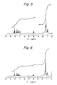
- Figures 4, 5, 6 and 7 show nuclear magnetic resonance spectra ('H-NMR) of liquid crystal compounds (4), (6), (8) and (12) in this invention which will be later described in Examples.
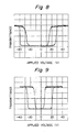
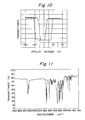
- Figures 8, 9 and 10 show optical response hysteresis of liquid crystal compounds (22), (24) and (26) in this invention which will be later described in Examples.
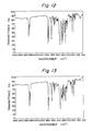
- Figures 11, 12, 13 and 14 show infrared absorption spectra of liquid crystal compounds (22), (24), (26) and (28) in this invention which will be later described in Examples.
- Figure 15 shows an optical response hysteresis of a liquid crystal compound (35) in this invention which will be later described in Examples.
- Figure 16 is an infrared absorption spectrum of the liquid crystal compound (35).
- Phase transition temperatures of the compound (4) in Example 1 are as follows. wherein a S X phase is an unidentified smectic phase.
- a liquid crystal cell (a cell thickness 3 micrometers) with an ITO electrode having a rubbed polyimide thin film was filled with the compound (4) in an isotropic phase.
- the cell was slowly cooled at a rate of 1.0°C per minute, and the liquid crystal was aligned in a S A phase.
- the cell was disposed between intersecting deflection plates such that the layer direction of the liquid crystal was parallel to an analyzer or a polarizer.
- a triangular wave voltage of +40V and 0.2 Hz was applied to the cell and the transmittance was measured by a photomultiplyer. As a result, a double hysteresis peculiar to the antiferroelectric phase was observed in a temeprature region of from 128°C to 74°C.
- Example 1 The procedure in 1) of Example 1 was repeated except that 14.0 g of n-octyl bromide was replaced with 16.2 g of n-decyl bromide. There resulted 9.2 g of the final compound (5).
- Example 2 The procedure in 4) of Example 1 was repeated except that 1.2 g of the compound (1) was replaced with 1.3 g of the compound (5). There was obtained 0.6 g of a final compound (6). A nuclear magnetic resonance spectrum ('H-NMR) of the final compound is shown in Figure 5. Identification of liquid crystal phases was carried out by observation of a texture and measurement by DSC.
- Phase transition temperatures of the compound (6) in Example 2 are shown as follows. wherein a S X phase is an unidentified smectic phase.
- Example 1 The procedure in 1) of Example 1 was repeated except that 14.0 g of n-octyl bromide was replaced with 18.2 g of n-dodecyl bromide. There resulted 14.6 g of a final compound (7).
- Example 2 The procedure in 4) of Example 1 was repeated except that 1.2 g of the compound (1) in Example 1 was replaced with 1.4 g of the compound (7). There was obtained 0.7 g of a final compound (8).
- a nuclear magnetic resonance spectrum ('H-NMR) of the final compound (8) is shown in Figure 6. Identification of phases was carried out by observation of a texture and measurement by DSC.
- Phase transition temperatures of the compound (8) in Example 3 are as follows.
- Example 1 The procedure in 1) of Example 1 was followed except 14.0 g of n-octyl bromide was replaced with 20.3 g of n-tetradecanol bromide. There was obtained 15.1 g of a final compound (11).
- Example 2 The procedure in 4) of Example 1 was followed except that 1.2 g of the compound (1) was replaced with 1.4 g of the compound (11). There was obtained 0.7 g of a final compound (12). A nuclear magnetic resonance spectrum (H'-NMR) of the final compound (12) is shown in Figure 7. Identification of phases was conducted by observation of a texture and measurement by DSC.
- Phase transition temperatures of the compound (12) in Example 4 are as follows.
- Example 1 The procedure in 1) of Example 1 was followed except that 14.0 g of n-octyl bromide was replaced with 13.2 g of n-heptyl bromide. There was obtained 11.1 g of a final compound (13).
- Phase transition temperatures of the compound (14) are as follows. There was no antiferroelectric phase.
- Example 1 The procedure in 1) of Example 1 was followed except that 14.0 g of n-octyl bromide was replaced with 15.2 g of n-nonyl bromide. There resulted 12.6 g of a final compound (15).
- Example 1 The procedure in 4) of Example 1 was followed except that 1.2 g of the compound (1) was replaced with 1.35 g of the compound (15). There was obtained 0.7 g of a final compound (16).
- Phase transition temperatures of the compound (16) are as follows. There was no antiferroelectric phase.
- Example 1 The procedure in 1) of Example 1 was followed except that 14.0 g of n-octyl bromide was replaced with 17.3 g of n-dodecyl bromide. There was obtained 14.5 g of a final compound (17).
- Example 1 The procedure in 4) of Example 1 was followed except that 1.2 g of the compound (1) in Example 1 was replaced with 1.4 g of the compound (17). There was obtained 0.4 g of a final compound (18).
- Phase transition temperatures of the compound (18) are as follows. There was no antiferroelectric phase. wherein a S X phase is an unidentified smectic phase.
- Example 1 The procedure in 1) of Example 1 was followed except that 14.0 g of n-octyl bromide was replaced with 13.0 g of n-heptyl bromide. There was obtained 12.5 g of a final compound (19).
- Phase transition temperatures of the compound (22) in Example 5 are as follows.
- Example 5 The procedure in 1) of Example 5 was followd except that 13.0 g of n-heptyl bromide was replaced with 14.0 g of n-octyl bromide. There was obtained 12.5 g of a final compound (23).
- Example 5 The procedure in 4) of Example 5 was followed except that 1.2 g of the compound (19) in Example 5 was replaced with 1.3 g of the compound (23). There resulted 1.1 g of a final compound (24). An infrared absorption spectrum (KBr) of the final compound is shown in Figure 12. Identification of phases was carried out by observation of a texture and measurement by DSC.
- Phase transition temperatures of the compound (24) in Example 6 are as follows.
- Example 5 The procedure in 4) of Example 5 was followed except that 1.2 g of the compound (19) in Example 5 was replaced with 1.3 g of the compound (25). There was obtained 0.9 g of a final compound (26). An infrared absorption spectrum (KBr) of the final compound is shown in Figure 13. Identification of phases was carried out by observation of a texture and measurement by DSC.
- Phase transition temperatures of the compound (26) in Example 7 are as follows.
- Example 5 The procedure in 1) of Example 5 was followed except that 13.0 g of n-heptyl bromide was replaced with 20.1 g of n-tetradecanyl bromide. There resulted 18.5 g of a final compound (27).
- Example 5 The procedure in 4) of Example 5 was followed except that 1.2 g of the compound (19) in Example 5 was replaced with 1.3 g of the compound (27). There resulted 0.9 g of the final compound (28). An infrared absorption spectrum (KBr) of the final compound (28) is shown in Figure 14. Identification of phases was carried out by observation of a texture and measurement by DSC.
- Phase transition temperatures of the compound (28) in Example 8 are as follows.
- the antiferroelectric phase of the compound (28) was in a supercooled state and unstable thermodynamically so that an optical response could not be observed. However, since an extinction direction was along the layer normal to the phase and a threshold was present, the antiferroelectric phase existed undoubtedly.
- Example 5 The procedure in 1) of Example 5 was followed except that 13.0 g of n-heptyl bromide was replaced with 12.0 g of n-hexyl bromide. There resulted 8.2 g of a final compound (29).
- Example 5 The procedure in 4) of Example 5 was followed except that 1.2 g of the compound (19) in Example 5 was replaced with 1.1 g of the compound (29). There resulted 0.8 g of a final compound (30).
- a series of phases of the compound (30) are as follows. There was no antiferroelectric phase.
- Example 5 The procedure in 1) of Example 5 was followed except that 13.0 g of n-heptyl bromide was replaced with 22.1 g of n-hexadecyl bromide. There resulted 16.4 g of a final compound (31).
- Example 5 The procedure in 4) of Example 5 was followed except that 1.2 g of the compound (19) was replaced with 1.45 g of the compound (31). There resulted 1.0 g of a final compound (32).
- a series of phases of the compound (32) are as follows. There was no antiferroelectric phase.
- Phase transition temperatures of the compound (35) are as follows.
- liquid crystal compounds represented by formula wherein m is 7, 9, 10, 11, 12 and 14, were prepared, and identification of phases was carried out by observation of a texture and measurement by DSC.
- the optical response of said liquid crystal compounds was measured in the same way as in 5) of Example 1, and a double hysteresis peculiar to the antiferro electric phase was observed.
- liquid crystal compounds represented by formula wherein m is 6 and 16 were prepared, and identification of phases was carried out by observation of a texture and measurement by DSC. The results are shown in Table 2. None of these liquid crystal compounds had the antiferroelectric phase.
Landscapes
- Chemical & Material Sciences (AREA)
- Organic Chemistry (AREA)
- Crystallography & Structural Chemistry (AREA)
- Engineering & Computer Science (AREA)
- Materials Engineering (AREA)
- Liquid Crystal Substances (AREA)
- Organic Low-Molecular-Weight Compounds And Preparation Thereof (AREA)
Applications Claiming Priority (6)
| Application Number | Priority Date | Filing Date | Title |
|---|---|---|---|
| JP88180/90 | 1990-04-04 | ||
| JP8818090 | 1990-04-04 | ||
| JP09405390A JP3262559B2 (ja) | 1990-04-11 | 1990-04-11 | 光学活性1―メチルペンチル基を有する液晶化合物 |
| JP94053/90 | 1990-04-11 | ||
| JP222543/90 | 1990-08-27 | ||
| JP2222543A JP2932638B2 (ja) | 1990-08-27 | 1990-08-27 | 光学活性1―メチルノニル基を有する液晶物質 |
Publications (2)
| Publication Number | Publication Date |
|---|---|
| EP0450595A1 true EP0450595A1 (fr) | 1991-10-09 |
| EP0450595B1 EP0450595B1 (fr) | 1995-03-01 |
Family
ID=27305757
Family Applications (1)
| Application Number | Title | Priority Date | Filing Date |
|---|---|---|---|
| EP91105252A Expired - Lifetime EP0450595B1 (fr) | 1990-04-04 | 1991-04-03 | Composé cristal liquide et dispositif d'affichage à cristaux liquides |
Country Status (3)
| Country | Link |
|---|---|
| US (1) | US5374375A (fr) |
| EP (1) | EP0450595B1 (fr) |
| DE (1) | DE69107646T2 (fr) |
Cited By (5)
| Publication number | Priority date | Publication date | Assignee | Title |
|---|---|---|---|---|
| EP0582519A1 (fr) * | 1992-08-06 | 1994-02-09 | Showa Shell Sekiyu Kabushiki Kaisha | Composition liquide cristalline, élément et dispositif l'utilisant |
| US5609790A (en) * | 1992-02-04 | 1997-03-11 | Seiko Epson Corporation | Liquid crystal compositions |
| EP0893429A1 (fr) * | 1997-07-23 | 1999-01-27 | Mitsubishi Gas Chemical Company, Inc. | Composé liquide cristallin ferriélectrique |
| EP0978504A1 (fr) * | 1998-08-07 | 2000-02-09 | Mitsubishi Gas Chemical Company, Inc. | Composé liquide cristallin antiferroélectrique |
| US6372308B1 (en) | 1999-01-28 | 2002-04-16 | Mitsubishi Gas Chemical Company Inc | Liquid crystal composition |
Families Citing this family (14)
| Publication number | Priority date | Publication date | Assignee | Title |
|---|---|---|---|---|
| JPH06334140A (ja) * | 1992-12-16 | 1994-12-02 | Ricoh Co Ltd | 強誘電体材料および該材料を用いた半導体メモリ、光記録媒体ならびに微小変位制御素子 |
| DE19509304A1 (de) * | 1994-03-16 | 1995-09-21 | Nippon Soken | Antiferroelektrische Flüssigkristallzusammensetzung |
| EP0676462A1 (fr) * | 1994-04-08 | 1995-10-11 | Nippon Soken, Inc. | Composition liquide cristalline ferro-électrique et élément indicateur la contenant |
| JPH07278059A (ja) * | 1994-04-08 | 1995-10-24 | Nippon Soken Inc | 反強誘電性液晶化合物 |
| JP3501866B2 (ja) * | 1994-07-19 | 2004-03-02 | 株式会社日本自動車部品総合研究所 | 反強誘電性液晶組成物及びそれを用いた液晶表示素子 |
| JP3052817B2 (ja) * | 1995-12-28 | 2000-06-19 | 株式会社日本自動車部品総合研究所 | 反強誘電性液晶組成物 |
| JPH1036844A (ja) * | 1996-07-25 | 1998-02-10 | Nippon Soken Inc | 反強誘電性液晶組成物 |
| JPH10130200A (ja) * | 1996-11-01 | 1998-05-19 | Mitsubishi Gas Chem Co Inc | 液晶中間体の製造法 |
| DE69801549T2 (de) * | 1997-06-20 | 2002-04-25 | Mitsubishi Gas Chemical Co., Inc. | Schwalbenschwanzförmige Flüssigkristallverbindung |
| US6870163B1 (en) | 1999-09-01 | 2005-03-22 | Displaytech, Inc. | Ferroelectric liquid crystal devices using materials with a de Vries smectic A phase |
| US7083832B2 (en) | 2000-09-01 | 2006-08-01 | Displaytech, Inc. | Partially fluorinated liquid crystal material |
| US7195719B1 (en) | 2001-01-03 | 2007-03-27 | Displaytech, Inc. | High polarization ferroelectric liquid crystal compositions |
| US6703082B1 (en) | 2001-06-20 | 2004-03-09 | Displaytech, Inc. | Bookshelf liquid crystal materials and devices |
| US6838128B1 (en) | 2002-02-05 | 2005-01-04 | Displaytech, Inc. | High polarization dopants for ferroelectric liquid crystal compositions |
Citations (3)
| Publication number | Priority date | Publication date | Assignee | Title |
|---|---|---|---|---|
| JPH01213390A (ja) * | 1988-02-22 | 1989-08-28 | Chisso Corp | 強誘電性液晶組成物および液晶表示素子 |
| EP0332392A2 (fr) * | 1988-03-09 | 1989-09-13 | Showa Shell Sekiyu Kabushiki Kaisha | Composés liquides cristallins dérivés du dioxane |
| EP0418604A1 (fr) * | 1989-08-28 | 1991-03-27 | Showa Shell Sekiyu Kabushiki Kaisha | Composé de cristal liquide |
Family Cites Families (14)
| Publication number | Priority date | Publication date | Assignee | Title |
|---|---|---|---|---|
| JPS6032748A (ja) * | 1983-07-29 | 1985-02-19 | Hitachi Ltd | 液晶性化合物 |
| EP0115693B1 (fr) * | 1983-01-06 | 1987-08-26 | Chisso Corporation | Composés cristaux liquides et mélanges de ceux-ci |
| US4647398A (en) * | 1984-02-03 | 1987-03-03 | Chisso Corporation | Liquid-crystalline carbonic acid esters and liquid crystal compositions containing same |
| JPH0662476B2 (ja) * | 1984-09-04 | 1994-08-17 | チッソ株式会社 | メチレンオキシ基を有する液晶性化合物及びその組成物 |
| US4943386A (en) * | 1985-01-09 | 1990-07-24 | Dainippon Ink & Chemicals, Inc. | Liquid crystalline compounds having substituents |
| EP0231853B1 (fr) * | 1986-01-31 | 1990-11-22 | Dainippon Ink And Chemicals, Inc. | Derivés optiquement actifs d'acides carboxyliques et compositions de cristaux liquides les contenant |
| JPH0643374B2 (ja) * | 1986-07-28 | 1994-06-08 | 高砂香料工業株式会社 | 液晶性化合物 |
| JPS63201147A (ja) * | 1987-02-17 | 1988-08-19 | Canon Inc | 液晶性化合物およびそれを含む液晶組成物 |
| US4906074A (en) * | 1987-09-28 | 1990-03-06 | Semiconductor Energy Laboratory Co., Ltd. | FLC liquid crystal electro-optical device having microdomains within pixels |
| US5171471A (en) * | 1988-03-09 | 1992-12-15 | Showa Shell Sekiyu K.K. | Dioxane liquid crystal compounds |
| KR900018725A (ko) * | 1988-05-12 | 1990-12-22 | 야마자끼 순페이 | 액정 전자 광학 장치 |
| US5078477A (en) * | 1988-11-09 | 1992-01-07 | Mitsubishi Gas Chemical Company, Inc. | Ferroelectric liquid crystal cell |
| JP2792729B2 (ja) * | 1989-10-11 | 1998-09-03 | シャープ株式会社 | 液晶素子 |
| JPH03223263A (ja) * | 1990-01-26 | 1991-10-02 | Showa Shell Sekiyu Kk | 液晶化合物 |
-
1991
- 1991-04-03 EP EP91105252A patent/EP0450595B1/fr not_active Expired - Lifetime
- 1991-04-03 DE DE69107646T patent/DE69107646T2/de not_active Expired - Fee Related
-
1992
- 1992-06-26 US US07/905,193 patent/US5374375A/en not_active Expired - Fee Related
Patent Citations (3)
| Publication number | Priority date | Publication date | Assignee | Title |
|---|---|---|---|---|
| JPH01213390A (ja) * | 1988-02-22 | 1989-08-28 | Chisso Corp | 強誘電性液晶組成物および液晶表示素子 |
| EP0332392A2 (fr) * | 1988-03-09 | 1989-09-13 | Showa Shell Sekiyu Kabushiki Kaisha | Composés liquides cristallins dérivés du dioxane |
| EP0418604A1 (fr) * | 1989-08-28 | 1991-03-27 | Showa Shell Sekiyu Kabushiki Kaisha | Composé de cristal liquide |
Non-Patent Citations (1)
| Title |
|---|
| CHEMICAL ABSTRACTS, vol. 109, no. 2, 11th July 1988, page 571, abstract no. 14938t Columbus, Ohio, US; & JP-A-62 273 284 (MATSUSHITA ELECTRIC IND. CO., LTD) 27-11-1987 * |
Cited By (7)
| Publication number | Priority date | Publication date | Assignee | Title |
|---|---|---|---|---|
| US5609790A (en) * | 1992-02-04 | 1997-03-11 | Seiko Epson Corporation | Liquid crystal compositions |
| EP0582519A1 (fr) * | 1992-08-06 | 1994-02-09 | Showa Shell Sekiyu Kabushiki Kaisha | Composition liquide cristalline, élément et dispositif l'utilisant |
| EP0893429A1 (fr) * | 1997-07-23 | 1999-01-27 | Mitsubishi Gas Chemical Company, Inc. | Composé liquide cristallin ferriélectrique |
| US5972243A (en) * | 1997-07-23 | 1999-10-26 | Mitsubishi Gas Chemical Company, Inc. | Ferrielectric liquid crystal compound |
| EP0978504A1 (fr) * | 1998-08-07 | 2000-02-09 | Mitsubishi Gas Chemical Company, Inc. | Composé liquide cristallin antiferroélectrique |
| US6133469A (en) * | 1998-08-07 | 2000-10-17 | Mitsubishi Gas Chemical Company | Anti-ferroelectric liquid crystal compound |
| US6372308B1 (en) | 1999-01-28 | 2002-04-16 | Mitsubishi Gas Chemical Company Inc | Liquid crystal composition |
Also Published As
| Publication number | Publication date |
|---|---|
| EP0450595B1 (fr) | 1995-03-01 |
| US5374375A (en) | 1994-12-20 |
| DE69107646D1 (de) | 1995-04-06 |
| DE69107646T2 (de) | 1995-08-24 |
Similar Documents
| Publication | Publication Date | Title |
|---|---|---|
| EP0450595B1 (fr) | Composé cristal liquide et dispositif d'affichage à cristaux liquides | |
| US4820444A (en) | 4'optically active alkoxy-4-alkoxy carbonyloxy-bipheneyl and mixtures thereof | |
| EP0487093B1 (fr) | Composé cristal liquide et dispositif d'affichage | |
| JPS62155257A (ja) | 強誘電性ピリジン化合物及び液晶組成物 | |
| US5938973A (en) | Swallow-tailed compound and ferrielectric liquid crystal composition containing the same | |
| EP0497297B1 (fr) | Composé cristal liquide et dispositif d'affichage à cristaux liquides | |
| US5972243A (en) | Ferrielectric liquid crystal compound | |
| US5976409A (en) | Swallow-tail-shaped liquid crystal compound | |
| EP0829469B1 (fr) | Composé racémique et composition liquide cristalline antiferroélectrique | |
| JPH09165356A (ja) | 反強誘電性液晶化合物及び反強誘電性液晶組成物 | |
| EP0484849B1 (fr) | Alcool optiquement actif, procédé pour sa production et composé crystal liquide en dérivant | |
| US5340498A (en) | Anti-ferroelectric liquid crystal and liquid crystal display device | |
| JP3262559B2 (ja) | 光学活性1―メチルペンチル基を有する液晶化合物 | |
| US5716544A (en) | Phenyl ester compound and liquid crystal composition containing the same | |
| US6217954B1 (en) | Phenyl triester compound and anti-ferroelectric liquid crystal composition containing the same | |
| JP2900599B2 (ja) | 液晶物質 | |
| JP2932638B2 (ja) | 光学活性1―メチルノニル基を有する液晶物質 | |
| JP3255180B2 (ja) | フッ素置換液晶物質 | |
| US6197389B1 (en) | Ferrielectric liquid crystal compound | |
| JP3470725B2 (ja) | 反強誘電性液晶物質および液晶表示素子 | |
| JPH0539246A (ja) | フツ素置換液晶物質 | |
| JPH04217942A (ja) | 光学活性1−メチルブチル基を有する液晶化合物 | |
| JPH0558959A (ja) | 液晶物質 | |
| JPS6163638A (ja) | 炭酸エステル液晶及びその組成物 | |
| JPH07316101A (ja) | 反強誘電性液晶物質 |
Legal Events
| Date | Code | Title | Description |
|---|---|---|---|
| PUAI | Public reference made under article 153(3) epc to a published international application that has entered the european phase |
Free format text: ORIGINAL CODE: 0009012 |
|
| AK | Designated contracting states |
Kind code of ref document: A1 Designated state(s): CH DE GB LI |
|
| 17P | Request for examination filed |
Effective date: 19911111 |
|
| 17Q | First examination report despatched |
Effective date: 19930602 |
|
| GRAA | (expected) grant |
Free format text: ORIGINAL CODE: 0009210 |
|
| AK | Designated contracting states |
Kind code of ref document: B1 Designated state(s): CH DE GB LI |
|
| REF | Corresponds to: |
Ref document number: 69107646 Country of ref document: DE Date of ref document: 19950406 |
|
| PLBE | No opposition filed within time limit |
Free format text: ORIGINAL CODE: 0009261 |
|
| STAA | Information on the status of an ep patent application or granted ep patent |
Free format text: STATUS: NO OPPOSITION FILED WITHIN TIME LIMIT |
|
| 26N | No opposition filed | ||
| PGFP | Annual fee paid to national office [announced via postgrant information from national office to epo] |
Ref country code: DE Payment date: 19980414 Year of fee payment: 8 |
|
| PGFP | Annual fee paid to national office [announced via postgrant information from national office to epo] |
Ref country code: GB Payment date: 19990408 Year of fee payment: 9 |
|
| PGFP | Annual fee paid to national office [announced via postgrant information from national office to epo] |
Ref country code: CH Payment date: 19990413 Year of fee payment: 9 |
|
| PG25 | Lapsed in a contracting state [announced via postgrant information from national office to epo] |
Ref country code: DE Free format text: LAPSE BECAUSE OF NON-PAYMENT OF DUE FEES Effective date: 20000201 |
|
| PG25 | Lapsed in a contracting state [announced via postgrant information from national office to epo] |
Ref country code: GB Free format text: LAPSE BECAUSE OF NON-PAYMENT OF DUE FEES Effective date: 20000403 |
|
| PG25 | Lapsed in a contracting state [announced via postgrant information from national office to epo] |
Ref country code: LI Free format text: LAPSE BECAUSE OF NON-PAYMENT OF DUE FEES Effective date: 20000430 Ref country code: CH Free format text: LAPSE BECAUSE OF NON-PAYMENT OF DUE FEES Effective date: 20000430 |
|
| GBPC | Gb: european patent ceased through non-payment of renewal fee |
Effective date: 20000403 |
|
| REG | Reference to a national code |
Ref country code: CH Ref legal event code: PL |