EP0460941B1 - Composition formant réserve et procédé de production d'un patron de réserve - Google Patents
Composition formant réserve et procédé de production d'un patron de réserve Download PDFInfo
- Publication number
- EP0460941B1 EP0460941B1 EP91305088A EP91305088A EP0460941B1 EP 0460941 B1 EP0460941 B1 EP 0460941B1 EP 91305088 A EP91305088 A EP 91305088A EP 91305088 A EP91305088 A EP 91305088A EP 0460941 B1 EP0460941 B1 EP 0460941B1
- Authority
- EP
- European Patent Office
- Prior art keywords
- resist
- pattern
- copolymer
- resist layer
- layer
- Prior art date
- Legal status (The legal status is an assumption and is not a legal conclusion. Google has not performed a legal analysis and makes no representation as to the accuracy of the status listed.)
- Expired - Lifetime
Links
Images


Classifications
-
- G—PHYSICS
- G03—PHOTOGRAPHY; CINEMATOGRAPHY; ANALOGOUS TECHNIQUES USING WAVES OTHER THAN OPTICAL WAVES; ELECTROGRAPHY; HOLOGRAPHY
- G03F—PHOTOMECHANICAL PRODUCTION OF TEXTURED OR PATTERNED SURFACES, e.g. FOR PRINTING, FOR PROCESSING OF SEMICONDUCTOR DEVICES; MATERIALS THEREFOR; ORIGINALS THEREFOR; APPARATUS SPECIALLY ADAPTED THEREFOR
- G03F7/00—Photomechanical, e.g. photolithographic, production of textured or patterned surfaces, e.g. printing surfaces; Materials therefor, e.g. comprising photoresists; Apparatus specially adapted therefor
- G03F7/004—Photosensitive materials
- G03F7/075—Silicon-containing compounds
- G03F7/0757—Macromolecular compounds containing Si-O, Si-C or Si-N bonds
- G03F7/0758—Macromolecular compounds containing Si-O, Si-C or Si-N bonds with silicon- containing groups in the side chains
-
- G—PHYSICS
- G03—PHOTOGRAPHY; CINEMATOGRAPHY; ANALOGOUS TECHNIQUES USING WAVES OTHER THAN OPTICAL WAVES; ELECTROGRAPHY; HOLOGRAPHY
- G03F—PHOTOMECHANICAL PRODUCTION OF TEXTURED OR PATTERNED SURFACES, e.g. FOR PRINTING, FOR PROCESSING OF SEMICONDUCTOR DEVICES; MATERIALS THEREFOR; ORIGINALS THEREFOR; APPARATUS SPECIALLY ADAPTED THEREFOR
- G03F7/00—Photomechanical, e.g. photolithographic, production of textured or patterned surfaces, e.g. printing surfaces; Materials therefor, e.g. comprising photoresists; Apparatus specially adapted therefor
- G03F7/004—Photosensitive materials
- G03F7/008—Azides
- G03F7/012—Macromolecular azides; Macromolecular additives, e.g. binders
- G03F7/0125—Macromolecular azides; Macromolecular additives, e.g. binders characterised by the polymeric binder or the macromolecular additives other than the macromolecular azides
-
- G—PHYSICS
- G03—PHOTOGRAPHY; CINEMATOGRAPHY; ANALOGOUS TECHNIQUES USING WAVES OTHER THAN OPTICAL WAVES; ELECTROGRAPHY; HOLOGRAPHY
- G03F—PHOTOMECHANICAL PRODUCTION OF TEXTURED OR PATTERNED SURFACES, e.g. FOR PRINTING, FOR PROCESSING OF SEMICONDUCTOR DEVICES; MATERIALS THEREFOR; ORIGINALS THEREFOR; APPARATUS SPECIALLY ADAPTED THEREFOR
- G03F7/00—Photomechanical, e.g. photolithographic, production of textured or patterned surfaces, e.g. printing surfaces; Materials therefor, e.g. comprising photoresists; Apparatus specially adapted therefor
- G03F7/16—Coating processes; Apparatus therefor
- G03F7/168—Finishing the coated layer, e.g. drying, baking, soaking
-
- Y—GENERAL TAGGING OF NEW TECHNOLOGICAL DEVELOPMENTS; GENERAL TAGGING OF CROSS-SECTIONAL TECHNOLOGIES SPANNING OVER SEVERAL SECTIONS OF THE IPC; TECHNICAL SUBJECTS COVERED BY FORMER USPC CROSS-REFERENCE ART COLLECTIONS [XRACs] AND DIGESTS
- Y10—TECHNICAL SUBJECTS COVERED BY FORMER USPC
- Y10S—TECHNICAL SUBJECTS COVERED BY FORMER USPC CROSS-REFERENCE ART COLLECTIONS [XRACs] AND DIGESTS
- Y10S430/00—Radiation imagery chemistry: process, composition, or product thereof
- Y10S430/143—Electron beam
Definitions
- the present invention relates to a positive-working resist composition for use in double layer resist processing.
- This integration is carried out by a miniaturization of unit elements and the use of a minimum line spacing of the wiring pattern on an order of submicrons, and further, a multi-layer wiring process is carried out. Therefore, many minute steps are formed on a semiconductor wafer when producing integrated circuits.
- a resist is coated on the semiconductor substrate, and then selectively exposed and developed to dissolve the exposed portions or unexposed portions, and finally, a through hole is formed. Thereafter, a photo-etching technique (photolithography or electron-beam lithography) is conducted, whereby a conductive film or an insulating film is etched by dry-etching.
- photo-etching technique photolithography or electron-beam lithography
- a multi-layer resist having a double-layer or triple-layer structure has been employed.
- a double-layer resist process having fewer process steps is generally employed.
- a novolac resist is coated on a substrate having steps, as a lower-layer resist providing a level surface, followed by coating a upper-layer resist thereon, which resist has an oxygen-plasma resistance and a high resolution.
- the molecular weight of the copolymer is from 20,000 to 1,500,000.
- a cross-linking of this resin at the R 3 position is caused by heating, but since it is necessary to enlarge the ratio of ⁇ -substituted acrylate having Si as a copolymer to improve the oxygen-plasma resistance, the cross-linking density becomes too low. Accordingly, the resolution is poor, and thus it is difficult to produce a fine pattern of 0.5 ⁇ m or less.
- JP-A-60138543 and JP-A-63307450 disclose a process for forming a resist pattern, wherein the resist is first cross-linked by heating a blend comprising an azide and an acrylate copolymer, and then selectively exposed to an electron beam in order to render soluble the exposed areas.
- the exposed areas are either vaporized or dissolved in a development solution.
- a novel resist composition according to this invention comprises a copolymer of formula (1) as defined above and, based on the weight of the copolymer, 0.1 to 30% by weight of an azide compound of any of formulae (2) to (7) and
- a process according to the invention, for forming a multi-level resist pattern comprises the steps of:
- the copolymer of formula (1) is heated (baked) to cause cross-linking, while splitting off R 3 as OH or NH 2 .
- the novel composition When the novel composition is heated (hard-baked) at a temperature higher than the decomposition temperature of the azide compound but lower than the decomposition temperature of the copolymer, the cross-linking density is increased, while forming the cross-linkage at a position other than that of R 3 .
- the temperature of heating is preferably above 130°C, and more preferably above 180°C.
- the azide compound is decomposed by the heat-treatment.
- the highly cross-linked copolymer when the highly cross-linked copolymer is subjected to electron beam radiation, the main chain is broken and becomes soluble in a solvent, as in the prior art.
- the polymer in the unexposed region is soluble, so that a strong developing agent such as methyl isobutyl ketone (MIBK) can be used, and resolution of a sub-micron pattern can be obtained.
- MIBK methyl isobutyl ketone
- the amount of the azide is 0.1 to 30% by weight of the copolymer. If the amount is less than 0.1%, the desired results cannot be obtained, and if the amount is more than 30%, the molecular weight becomes too large due to extensive cross-linking, so that complete decomposition cannot be obtained even by electron beam radiation, so that a positive resist pattern cannot be obtained.
- 4,4'-diazide chalcone of the formula (2) was used as an azide compound and this azide was added to the copolymer at the ratio of 5 weight% based on the polymer, then mixed with a MIBK solution at a ratio of 30 grams/l to form a resist.
- This resist was coated on a silicon wafer to a thickness of about 3000 ⁇ , then heated on a hot plate for eight minutes at 220°C.
- the formed resist film was exposed to an electron beam with an accelerated voltage of 20 KeV, and developed for three minutes in MIBK, 0.4 micron patterns were resolved.
- the sensitivity (E th) was 14.4 ⁇ C/cm 2 .
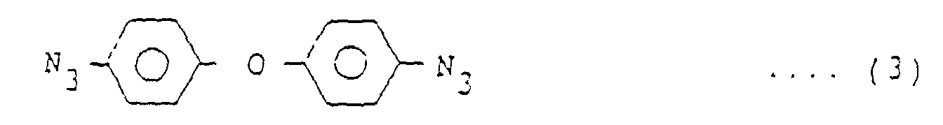
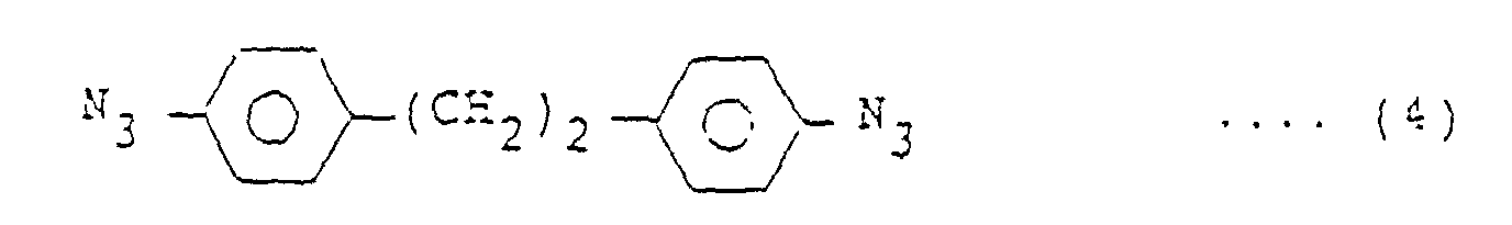
- the copolymer of the formula (8) was used, and as an azide compound, the compounds of the formulas (3) to (7) were respectively used, to obtain a resist in the same way as in Example 1.
- the thus obtained resist was coated on a silicon wafer to a thickness of about 3000 ⁇ and a similar procedure as in Example 1 effected, to obtain similar effects.
- the thus obtained resist was coated on a silicon wafer to a thickness of 3000 ⁇ , followed by heating on a hot-plate for eight minutes at a predetermined temperature.
- the resist layer was exposed to an electron beam at an accelerated voltage of 20 KeV, and developed for three minutes in MIBK, 0.3 micron patterns were resolved.
- the sensitivity (E th) was 11.2 ⁇ C/cm 2 .
- the copolymer of the formula (9) was used and as a diazide compound, the compounds of the formulas (3) through (7) were respectively used to form a resist.
- the copolymer of the formula (10) was used, and as a diazide compound, the compounds of the formulas (3) through (7) were respectively used to form a resist.
- a novolac-type photo resist (manufactured by Nagase Sangyo Co., Ltd.) 3 was coated to a thickness of 2.0 ⁇ m on a substrate 1, with a step having an aluminum wire 2 therein (Fig. 1A, Fig. 1B), and baked at a temperature of 220°C in an oven to form a lower resist layer.
- a 30 g/l MIBK resist solution 4 for an upper layer comprising the copolymer of the formula (8) and 5 weight% of 4,4'-diazide chalcone was coated on the substrate 1 (Fig. 1C), followed by baking at a temperature of 220°C on a hot plate for eight minutes.
- the thus formed resist layer was exposed to an electron beam at an accelerated voltage of 20 KeV to form a 0.4 ⁇ m line and space pattern (Fig. 1D), which was developed in MIBK for two minutes to obtain an upper resist pattern 5 (Fig. 1E).
- This upper resist layer was resistant to oxygen plasma.
- the lower resist layer was etched by oxygen-reactive ion etching (RIE) using the thus-obtained upper resist layer as a mask, to form a 0.4 ⁇ m line and space lower resist pattern (Fig. 1F).
- RIE oxygen-reactive ion etching
- the substrate 1 was dry-etched using the upper and lower resists layers as a mask (Fig. 1G), followed by removing both resist layers to obtain a contact hole 6 (Fig. 1H).
Landscapes
- Physics & Mathematics (AREA)
- Spectroscopy & Molecular Physics (AREA)
- General Physics & Mathematics (AREA)
- Exposure And Positioning Against Photoresist Photosensitive Materials (AREA)
- Photosensitive Polymer And Photoresist Processing (AREA)
Claims (4)
- Composition de réserve, qui comprend:sur base du poids du copolymère, 0,1 à 30% en poids d'un composé azide de l'une quelconque des formules (2) à (7).un copolymère de formule (1):dans laquelle R1 représente CH3, CF3, CN, CH2OH ou CH2COR où R représente un alkyle en C1-5,
 R2 représente un radical hydrocarboné comptant au moins un atome de Si,R3 représente OH, OC(CH3)3, NH2 ou NHCH2OH, etm et n représentent chacun un entier avec n/m ≤1; et
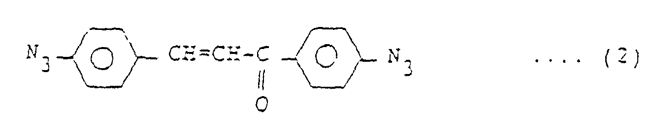
 et
et

- Procédé de formation d'une structure de réserve à plusieurs couches, qui comprend les étapes consistant à:revêtir un substrat semi-conducteur d'une réserve, pour former sur lui une couche inférieure de réserve;revêtir la couche inférieure de réserve d'une composition de réserve selon la revendication 1, pour former sur elle une couche supérieure de réserve;chauffer le substrat, à une température supérieure à la température de décomposition du composé azide, et inférieure à la température de décomposition du copolymère, pour produire une réticulation de la couche supérieure de réserve;exposer la réserve à un rayonnement par faisceau d'électrons selon un motif prédéterminé, pour former dans la couche de réserve une image latente correspondant au motif du rayonnement; etdévelopper la couche de réserve exposée à la forme du motif à l'aide d'un révélateur, pour former un motif supérieur de réserve.
- Procédé selon la revendication 2, qui comprend de plus la cuisson de la couche inférieure de réserve.
- Procédé selon la revendication 2 ou la revendication 3, dans lequel ladite température est supérieure à 130°C.
Applications Claiming Priority (2)
| Application Number | Priority Date | Filing Date | Title |
|---|---|---|---|
| JP2150820A JPH0442229A (ja) | 1990-06-08 | 1990-06-08 | レジスト材料およびパターンの形成方法 |
| JP150820/90 | 1990-06-08 |
Publications (3)
| Publication Number | Publication Date |
|---|---|
| EP0460941A2 EP0460941A2 (fr) | 1991-12-11 |
| EP0460941A3 EP0460941A3 (en) | 1992-09-16 |
| EP0460941B1 true EP0460941B1 (fr) | 1998-09-02 |
Family
ID=15505125
Family Applications (1)
| Application Number | Title | Priority Date | Filing Date |
|---|---|---|---|
| EP91305088A Expired - Lifetime EP0460941B1 (fr) | 1990-06-08 | 1991-06-05 | Composition formant réserve et procédé de production d'un patron de réserve |
Country Status (4)
| Country | Link |
|---|---|
| US (1) | US5326670A (fr) |
| EP (1) | EP0460941B1 (fr) |
| JP (1) | JPH0442229A (fr) |
| DE (1) | DE69130084T2 (fr) |
Families Citing this family (9)
| Publication number | Priority date | Publication date | Assignee | Title |
|---|---|---|---|---|
| JPH06332196A (ja) * | 1993-05-24 | 1994-12-02 | Nippon Paint Co Ltd | レジストパターンの形成方法 |
| JP2980149B2 (ja) * | 1993-09-24 | 1999-11-22 | 富士通株式会社 | レジスト材料およびパターン形成方法 |
| US5705309A (en) * | 1996-09-24 | 1998-01-06 | Eastman Kodak Company | Photosensitive composition and element containing polyazide and an infrared absorber in a photocrosslinkable binder |
| US5985524A (en) * | 1997-03-28 | 1999-11-16 | International Business Machines Incorporated | Process for using bilayer photoresist |
| US6358675B1 (en) | 1998-10-02 | 2002-03-19 | 3M Innovative Properties Company | Silicon-containing alcohols and polymers having silicon-containing tertiary ester groups made therefrom |
| TWI294440B (fr) * | 2000-02-16 | 2008-03-11 | Shinetsu Chemical Co | |
| US6683202B2 (en) | 2001-02-22 | 2004-01-27 | Tokyo Ohka, Kogyo Co., Ltd. | Fluorine-containing monomeric ester compound for base resin in photoresist composition |
| FR2841900B1 (fr) * | 2002-07-08 | 2007-03-02 | Genfit S A | Nouveaux derives de 1,3-diphenylprop-2-en-1-one substitues, preparation et utilisations |
| FR2841784B1 (fr) | 2002-07-08 | 2007-03-02 | Composition a base de derives de 1,3-diphenylprop-2en-1-one substitues, preparation et utilisations |
Citations (1)
| Publication number | Priority date | Publication date | Assignee | Title |
|---|---|---|---|---|
| EP0447111A1 (fr) * | 1990-03-13 | 1991-09-18 | Fujitsu Limited | Composition de photorésiste et procédé de formation de micro-motifs |
Family Cites Families (11)
| Publication number | Priority date | Publication date | Assignee | Title |
|---|---|---|---|---|
| NL7906932A (nl) * | 1979-09-18 | 1981-03-20 | Philips Nv | Negatief resist-materiaal, drager met resist-materiaal en werkwijze voor het volgens een patroon aanbrengen van een laag. |
| JPS56139515A (en) * | 1980-03-31 | 1981-10-31 | Daikin Ind Ltd | Polyfluoroalkyl acrylate copolymer |
| DE3280230D1 (de) * | 1981-05-07 | 1990-09-20 | Honeywell Inc | Verfahren zur herstellung von empfindlichen positiven elektronenstrahlresists. |
| EP0090089B1 (fr) * | 1981-12-19 | 1988-10-05 | Daikin Kogyo Co., Ltd. | Matériau pour photoréserve et procédé pour la formation d'un patron de réserve fin |
| US4476217A (en) * | 1982-05-10 | 1984-10-09 | Honeywell Inc. | Sensitive positive electron beam resists |
| JPS60254041A (ja) * | 1984-05-30 | 1985-12-14 | Fujitsu Ltd | パタ−ン形成方法 |
| US4788127A (en) * | 1986-11-17 | 1988-11-29 | Eastman Kodak Company | Photoresist composition comprising an interpolymer of a silicon-containing monomer and an hydroxystyrene |
| JPH02115853A (ja) * | 1988-10-26 | 1990-04-27 | Fujitsu Ltd | 半導体装置の製造方法 |
| JP2653148B2 (ja) * | 1989-01-20 | 1997-09-10 | 富士通株式会社 | レジスト組成物 |
| JP2737225B2 (ja) * | 1989-03-27 | 1998-04-08 | 松下電器産業株式会社 | 微細パターン形成材料およびパターン形成方法 |
| JP2659025B2 (ja) * | 1990-01-24 | 1997-09-30 | 富士通株式会社 | 放射線用レジスト及びその製造方法及びパターン形成方法 |
-
1990
- 1990-06-08 JP JP2150820A patent/JPH0442229A/ja active Pending
-
1991
- 1991-06-05 DE DE69130084T patent/DE69130084T2/de not_active Expired - Fee Related
- 1991-06-05 EP EP91305088A patent/EP0460941B1/fr not_active Expired - Lifetime
- 1991-06-07 US US07/711,779 patent/US5326670A/en not_active Expired - Fee Related
Patent Citations (1)
| Publication number | Priority date | Publication date | Assignee | Title |
|---|---|---|---|---|
| EP0447111A1 (fr) * | 1990-03-13 | 1991-09-18 | Fujitsu Limited | Composition de photorésiste et procédé de formation de micro-motifs |
Also Published As
| Publication number | Publication date |
|---|---|
| EP0460941A3 (en) | 1992-09-16 |
| US5326670A (en) | 1994-07-05 |
| EP0460941A2 (fr) | 1991-12-11 |
| DE69130084D1 (de) | 1998-10-08 |
| JPH0442229A (ja) | 1992-02-12 |
| DE69130084T2 (de) | 1999-01-21 |
Similar Documents
| Publication | Publication Date | Title |
|---|---|---|
| US4863833A (en) | Pattern-forming material and its production and use | |
| US4908298A (en) | Method of creating patterned multilayer films for use in production of semiconductor circuits and systems | |
| EP0543762B1 (fr) | Compositions de photoréserve développable par voie sèche et méthode d'utilisation | |
| EP0069854B1 (fr) | Méthode pour la formation de trous de passage dans des couches isolantes | |
| EP0130338A2 (fr) | Structure réserve, procédé pour la fabrication et la formation de l'image | |
| EP0492256B1 (fr) | Création de structure par voie photolithographique | |
| EP0460941B1 (fr) | Composition formant réserve et procédé de production d'un patron de réserve | |
| US4968583A (en) | Pattern forming method employing electron beam lithography | |
| JP2707785B2 (ja) | レジスト組成物およびパターン形成方法 | |
| US5194364A (en) | Process for formation of resist patterns | |
| JPH07113773B2 (ja) | パタ−ン形成方法 | |
| KR930010221B1 (ko) | 도전성 화합물을 이용한 패턴 형성 방법 | |
| EP0333591B1 (fr) | Procédé pour l'obtention d'un modèle de réserve | |
| US4968582A (en) | Photoresists resistant to oxygen plasmas | |
| EP0195291B1 (fr) | Procédé pour obtenir des surfaces texturées dans des films multicouches et emploi dans la fabrication de circuits et systèmes semi-conducteurs | |
| US5114827A (en) | Photoresists resistant to oxygen plasmas | |
| EP0199303B1 (fr) | Procédé pour obtenir des structures formant un agent de photoréserve | |
| EP0449439A1 (fr) | Procédé pour la formation des résists | |
| JPH08193167A (ja) | 感光性樹脂組成物 | |
| JPH05216232A (ja) | レジスト組成物とレジストパターンの形成方法 | |
| JPH0795509B2 (ja) | レジストパタ−ンの形成方法 | |
| EP0250762B1 (fr) | Préparation de films et de couches de polymères, perméables par lixiviation | |
| JP2725351B2 (ja) | X線レジスト組成物 | |
| JPH0313947A (ja) | レジストパターンの形成方法 | |
| JPH04294355A (ja) | レジスト組成物とレジストパターンの形成方法 |
Legal Events
| Date | Code | Title | Description |
|---|---|---|---|
| PUAI | Public reference made under article 153(3) epc to a published international application that has entered the european phase |
Free format text: ORIGINAL CODE: 0009012 |
|
| AK | Designated contracting states |
Kind code of ref document: A2 Designated state(s): DE FR GB |
|
| PUAL | Search report despatched |
Free format text: ORIGINAL CODE: 0009013 |
|
| AK | Designated contracting states |
Kind code of ref document: A3 Designated state(s): DE FR GB |
|
| 17P | Request for examination filed |
Effective date: 19921028 |
|
| 17Q | First examination report despatched |
Effective date: 19960913 |
|
| GRAG | Despatch of communication of intention to grant |
Free format text: ORIGINAL CODE: EPIDOS AGRA |
|
| GRAG | Despatch of communication of intention to grant |
Free format text: ORIGINAL CODE: EPIDOS AGRA |
|
| GRAH | Despatch of communication of intention to grant a patent |
Free format text: ORIGINAL CODE: EPIDOS IGRA |
|
| GRAH | Despatch of communication of intention to grant a patent |
Free format text: ORIGINAL CODE: EPIDOS IGRA |
|
| GRAA | (expected) grant |
Free format text: ORIGINAL CODE: 0009210 |
|
| AK | Designated contracting states |
Kind code of ref document: B1 Designated state(s): DE FR GB |
|
| PG25 | Lapsed in a contracting state [announced via postgrant information from national office to epo] |
Ref country code: FR Free format text: LAPSE BECAUSE OF FAILURE TO SUBMIT A TRANSLATION OF THE DESCRIPTION OR TO PAY THE FEE WITHIN THE PRESCRIBED TIME-LIMIT Effective date: 19980902 |
|
| REF | Corresponds to: |
Ref document number: 69130084 Country of ref document: DE Date of ref document: 19981008 |
|
| EN | Fr: translation not filed | ||
| PG25 | Lapsed in a contracting state [announced via postgrant information from national office to epo] |
Ref country code: GB Free format text: LAPSE BECAUSE OF NON-PAYMENT OF DUE FEES Effective date: 19990605 |
|
| PLBE | No opposition filed within time limit |
Free format text: ORIGINAL CODE: 0009261 |
|
| STAA | Information on the status of an ep patent application or granted ep patent |
Free format text: STATUS: NO OPPOSITION FILED WITHIN TIME LIMIT |
|
| PGFP | Annual fee paid to national office [announced via postgrant information from national office to epo] |
Ref country code: DE Payment date: 19990812 Year of fee payment: 9 |
|
| 26N | No opposition filed | ||
| GBPC | Gb: european patent ceased through non-payment of renewal fee |
Effective date: 19990605 |
|
| PG25 | Lapsed in a contracting state [announced via postgrant information from national office to epo] |
Ref country code: DE Free format text: LAPSE BECAUSE OF NON-PAYMENT OF DUE FEES Effective date: 20010403 |