EP0465230B1 - Sous-ensemble à base de silicium - Google Patents
Sous-ensemble à base de silicium Download PDFInfo
- Publication number
- EP0465230B1 EP0465230B1 EP91306016A EP91306016A EP0465230B1 EP 0465230 B1 EP0465230 B1 EP 0465230B1 EP 91306016 A EP91306016 A EP 91306016A EP 91306016 A EP91306016 A EP 91306016A EP 0465230 B1 EP0465230 B1 EP 0465230B1
- Authority
- EP
- European Patent Office
- Prior art keywords
- optical
- silicon substrate
- subassembly
- opening
- lens
- Prior art date
- Legal status (The legal status is an assumption and is not a legal conclusion. Google has not performed a legal analysis and makes no representation as to the accuracy of the status listed.)
- Expired - Lifetime
Links
Images


Classifications
-
- G—PHYSICS
- G02—OPTICS
- G02B—OPTICAL ELEMENTS, SYSTEMS OR APPARATUS
- G02B6/00—Light guides; Structural details of arrangements comprising light guides and other optical elements, e.g. couplings
- G02B6/10—Light guides; Structural details of arrangements comprising light guides and other optical elements, e.g. couplings of the optical waveguide type
- G02B6/12—Light guides; Structural details of arrangements comprising light guides and other optical elements, e.g. couplings of the optical waveguide type of the integrated circuit kind
- G02B6/12004—Combinations of two or more optical elements
-
- G—PHYSICS
- G02—OPTICS
- G02B—OPTICAL ELEMENTS, SYSTEMS OR APPARATUS
- G02B6/00—Light guides; Structural details of arrangements comprising light guides and other optical elements, e.g. couplings
- G02B6/24—Coupling light guides
- G02B6/42—Coupling light guides with opto-electronic elements
- G02B6/4201—Packages, e.g. shape, construction, internal or external details
- G02B6/4204—Packages, e.g. shape, construction, internal or external details the coupling comprising intermediate optical elements, e.g. lenses, holograms
- G02B6/4207—Packages, e.g. shape, construction, internal or external details the coupling comprising intermediate optical elements, e.g. lenses, holograms with optical elements reducing the sensitivity to optical feedback
- G02B6/4208—Packages, e.g. shape, construction, internal or external details the coupling comprising intermediate optical elements, e.g. lenses, holograms with optical elements reducing the sensitivity to optical feedback using non-reciprocal elements or birefringent plates, i.e. quasi-isolators
-
- G—PHYSICS
- G02—OPTICS
- G02B—OPTICAL ELEMENTS, SYSTEMS OR APPARATUS
- G02B6/00—Light guides; Structural details of arrangements comprising light guides and other optical elements, e.g. couplings
- G02B6/24—Coupling light guides
- G02B6/42—Coupling light guides with opto-electronic elements
- G02B6/4201—Packages, e.g. shape, construction, internal or external details
- G02B6/4219—Mechanical fixtures for holding or positioning the elements relative to each other in the couplings; Alignment methods for the elements, e.g. measuring or observing methods especially used therefor
- G02B6/4228—Passive alignment, i.e. without a detection of the degree of coupling or the position of the elements
- G02B6/423—Passive alignment, i.e. without a detection of the degree of coupling or the position of the elements using guiding surfaces for the alignment
-
- G—PHYSICS
- G02—OPTICS
- G02B—OPTICAL ELEMENTS, SYSTEMS OR APPARATUS
- G02B6/00—Light guides; Structural details of arrangements comprising light guides and other optical elements, e.g. couplings
- G02B6/24—Coupling light guides
- G02B6/42—Coupling light guides with opto-electronic elements
- G02B6/43—Arrangements comprising a plurality of opto-electronic elements and associated optical interconnections
-
- G—PHYSICS
- G02—OPTICS
- G02B—OPTICAL ELEMENTS, SYSTEMS OR APPARATUS
- G02B7/00—Mountings, adjusting means, or light-tight connections, for optical elements
-
- H—ELECTRICITY
- H01—ELECTRIC ELEMENTS
- H01S—DEVICES USING THE PROCESS OF LIGHT AMPLIFICATION BY STIMULATED EMISSION OF RADIATION [LASER] TO AMPLIFY OR GENERATE LIGHT; DEVICES USING STIMULATED EMISSION OF ELECTROMAGNETIC RADIATION IN WAVE RANGES OTHER THAN OPTICAL
- H01S5/00—Semiconductor lasers
- H01S5/02—Structural details or components not essential to laser action
- H01S5/022—Mountings; Housings
- H01S5/0235—Method for mounting laser chips
- H01S5/02375—Positioning of the laser chips
-
- H—ELECTRICITY
- H10—SEMICONDUCTOR DEVICES; ELECTRIC SOLID-STATE DEVICES NOT OTHERWISE PROVIDED FOR
- H10W—GENERIC PACKAGES, INTERCONNECTIONS, CONNECTORS OR OTHER CONSTRUCTIONAL DETAILS OF DEVICES COVERED BY CLASS H10
- H10W90/00—Package configurations
-
- H—ELECTRICITY
- H01—ELECTRIC ELEMENTS
- H01S—DEVICES USING THE PROCESS OF LIGHT AMPLIFICATION BY STIMULATED EMISSION OF RADIATION [LASER] TO AMPLIFY OR GENERATE LIGHT; DEVICES USING STIMULATED EMISSION OF ELECTROMAGNETIC RADIATION IN WAVE RANGES OTHER THAN OPTICAL
- H01S5/00—Semiconductor lasers
- H01S5/02—Structural details or components not essential to laser action
- H01S5/0206—Substrates, e.g. growth, shape, material, removal or bonding
- H01S5/021—Silicon based substrates
-
- H—ELECTRICITY
- H01—ELECTRIC ELEMENTS
- H01S—DEVICES USING THE PROCESS OF LIGHT AMPLIFICATION BY STIMULATED EMISSION OF RADIATION [LASER] TO AMPLIFY OR GENERATE LIGHT; DEVICES USING STIMULATED EMISSION OF ELECTROMAGNETIC RADIATION IN WAVE RANGES OTHER THAN OPTICAL
- H01S5/00—Semiconductor lasers
- H01S5/02—Structural details or components not essential to laser action
- H01S5/022—Mountings; Housings
- H01S5/0225—Out-coupling of light
- H01S5/02253—Out-coupling of light using lenses
-
- H—ELECTRICITY
- H01—ELECTRIC ELEMENTS
- H01S—DEVICES USING THE PROCESS OF LIGHT AMPLIFICATION BY STIMULATED EMISSION OF RADIATION [LASER] TO AMPLIFY OR GENERATE LIGHT; DEVICES USING STIMULATED EMISSION OF ELECTROMAGNETIC RADIATION IN WAVE RANGES OTHER THAN OPTICAL
- H01S5/00—Semiconductor lasers
- H01S5/02—Structural details or components not essential to laser action
- H01S5/022—Mountings; Housings
- H01S5/023—Mount members, e.g. sub-mount members
- H01S5/02325—Mechanically integrated components on mount members or optical micro-benches
-
- H—ELECTRICITY
- H01—ELECTRIC ELEMENTS
- H01S—DEVICES USING THE PROCESS OF LIGHT AMPLIFICATION BY STIMULATED EMISSION OF RADIATION [LASER] TO AMPLIFY OR GENERATE LIGHT; DEVICES USING STIMULATED EMISSION OF ELECTROMAGNETIC RADIATION IN WAVE RANGES OTHER THAN OPTICAL
- H01S5/00—Semiconductor lasers
- H01S5/02—Structural details or components not essential to laser action
- H01S5/024—Arrangements for thermal management
- H01S5/02407—Active cooling, e.g. the laser temperature is controlled by a thermo-electric cooler or water cooling
- H01S5/02415—Active cooling, e.g. the laser temperature is controlled by a thermo-electric cooler or water cooling by using a thermo-electric cooler [TEC], e.g. Peltier element
-
- H—ELECTRICITY
- H01—ELECTRIC ELEMENTS
- H01S—DEVICES USING THE PROCESS OF LIGHT AMPLIFICATION BY STIMULATED EMISSION OF RADIATION [LASER] TO AMPLIFY OR GENERATE LIGHT; DEVICES USING STIMULATED EMISSION OF ELECTROMAGNETIC RADIATION IN WAVE RANGES OTHER THAN OPTICAL
- H01S5/00—Semiconductor lasers
- H01S5/02—Structural details or components not essential to laser action
- H01S5/024—Arrangements for thermal management
- H01S5/02438—Characterized by cooling of elements other than the laser chip, e.g. an optical element being part of an external cavity or a collimating lens
-
- Y—GENERAL TAGGING OF NEW TECHNOLOGICAL DEVELOPMENTS; GENERAL TAGGING OF CROSS-SECTIONAL TECHNOLOGIES SPANNING OVER SEVERAL SECTIONS OF THE IPC; TECHNICAL SUBJECTS COVERED BY FORMER USPC CROSS-REFERENCE ART COLLECTIONS [XRACs] AND DIGESTS
- Y10—TECHNICAL SUBJECTS COVERED BY FORMER USPC
- Y10S—TECHNICAL SUBJECTS COVERED BY FORMER USPC CROSS-REFERENCE ART COLLECTIONS [XRACs] AND DIGESTS
- Y10S257/00—Active solid-state devices, e.g. transistors, solid-state diodes
- Y10S257/93—Thermoelectric, e.g. peltier effect cooling
Definitions
- the present invention relates to a silicon-based optical subassembly and, more particularly, to an optical subassembly including a silicon substrate with a plurality of etched openings for positioning of various optical components.
- Semiconductor optical devices such as lasers are used in a wide variety of applications, due to their compactness, relatively high efficiency, and well-controlled output.
- a number of requirements are imposed upon these devices.
- cooling of the optical device is often necessary, since prolonged high temperature operation can seriously damage and even destroy the device.
- the output light intensity from the device is a function of its junction temperature, the supporting structure must be able to efficiently dissipate the heat generated by the high current density in the device in its operating state.
- the supporting structure may comprise a number of different members.
- a conventional optical subassembly may utilize one member for the active (e.g., laser) device and a separate member for the passive components. Alignment between the two members is thus required to achieve the desired minimum level of acceptable coupling loss.
- a single mounting member may be used to hold all the required optical components. In the latter arrangement, each mounting member is individually formed, using precision die-cast piece parts, for example. Additionally, active alignment operations are often required as each component is affixed to the mounting member.
- the optical subassembly is often a relatively expensive component of a lightwave transmitter, requiring a relatively long, expensive and tedious assembly process. Further, any modifications in the size, number or arrangement of the optical components often necessitates a redesign of the complete optical subassembly.
- an optical subassembly which is robust in design, relatively simple to assemble (i.e., requiring few, if any, active alignments), and more amenable to high-volume, low-cost manufacture than those available in the prior art. Further, a need remains for an optical subassembly, including an isolator, which is capable of efficiently controlling the temperature of both the laser and the isolator.
- the present invention relates to an optical subassembly and, more particularly, to a silicon-based subassembly including a plurality of etched openings for positioning of various optical components according to claims 1 and 20.
- a silicon substrate is processed to form a plurality of openings for placement of the required optical components.
- the silicon substrate is etched to include a fist opening for placement of a first (e.g., subassembly-to-fiber coupling) lens, a second opening for placement of isolator optics, and a third opening for placement of a second (e.g., laser-to-isolator coupling) lens.
- a fourth opening for placement of a laser diode chip carrier may also be included.
- a silicon wafer may be patterned and etched to simultaneously form hundreds of subassemblies.
- the second opening (for the isolator) may be eliminated - this design is especially suited for low speed applications where isolation of the laser from the remaining components is not necessary.
- this second opening may be used to hold other passive optical components, such as a third lens or filter.
- the isolator optics are included on the same substrate as the laser such that both components are cooled by the same thermoelectric cooler (TEC) so as to operate at the same (controlled) temperature. Additionally, the isolator's magnet is thermally separated from the remaining elements forming the optical subassembly. As mentioned above, the cooling of the magnet in prior art designs is not necessary and only serves to increase the cooling load on the TEC. Thermal separation is achieved in accordance with one aspect of the present invention by supporting the silicon substrate in the cantilever arrangement so as to pass through the open core region of the isolator's magnet in a manner such that physical contact between the magnet and substrate is avoided.
- a support member attached to the underside of the substrate in the vicinity of the laser, is used to form the cantilever arrangement with the substrate and prevent physical contact between the silicon substrate and the magnet.
- the support member is the thermoelectric cooler (TEC) which is advantageously attached to the underside of the silicon substrate in the vicinity of the laser diode and isolator optical component.
- TEC thermoelectric cooler
- the use of silicon as the submount material provides for relatively quick transport of temperature changes from the TEC through the substrate to the laser and isolator optics.
- etching process used to form the openings is relatively simple and may be controlled so as to provide the required optical alignment between the various components placed in the openings without the need to perform timely (and costly) active alignments subsequent to assembly.
- a further advantage is that the submount (the silicon substrate) may be redesigned merely by changing the masks used to delineate the locations of the various openings.
- the silicon substrate used to hold the various optical components will be referred to as the "submount”; the arrangement including the submount and the various optical components attached thereto will be referred to as the "optical subassembly", or simply, the “subassembly”.
- FIG. 1 contains a view in perspective of an exemplary silicon-based optical submount 10 formed in accordance with the present invention.
- submount 10 comprises a silicon substrate 11 which is processed to include a plurality of openings, formed in top surface 13 thereof, for the placement of a plurality of optical devices.
- silicon substrate 11 is formed to include a first opening 12 for placement of a first lens.
- opening 12 is formed as a rectangular trapezoid, with sidewalls 14,16 which slant inwardly towards a bottom surface 18. Opening 12 is so formed with predetermined dimensions appropriate for placement therein of a cylindrically-shaped graded-index (GRIN) lens (FIG.
- GRIN cylindrically-shaped graded-index
- a second lens for example, a spherical lens which is used to collimate the optical signal exiting an active optical device (e.g., laser).
- Second opening 20 is formed to comprise suitable dimensions such that the input beam from the active device will intercept a spherical lens in a manner such that the lens will form a collimated output signal.
- a third opening 22 is formed between first opening 12 and second opening 20, along the z-axis of substrate 11 as shown in FIG. 1.
- Third opening 22 also comprises a rectangular trapezoidal shape, with side faces 24, 26 sloping inwardly towards a bottom surface 28.
- Opening 22 may be used, as shown in later figures, to hold the optical component portion of an optical isolator.
- an optical isolator may be used in high bit rate applications where it is desired to prevent any significant reflections from re-entering the laser active region.
- the physical dimensions of the isolator are somewhat smaller than those of the GRIN lens. Therefore, opening 22 is somewhat smaller than opening 12.
- a fourth, relatively shallow opening 22 may be located behind opening 20. Opening 30 is utilized for placement of the chip carrier holding the active optical device. In an alternative embodiment, the chip carrier may be attached directly to top surface 13 of substrate 11.
- FIG. 2 contains a view in perspective of an optical subassembly 32 utilizing the silicon-based submount 10 of FIG. 1.
- a GRIN lens 34 and spherical lens 36 are placed in and attached to openings 12 and 20, respectively, using, for example, a glass solder.
- the tapered sidewalls of openings 12,20 provide for physical contact for the edges thereof. to silicon substrate 11.
- a chip carrier 38, holding a pre-bonded laser 40, is next aligned with and soldered to a metal contact deposited in opening 30 (or alternatively, mounted directly on substrate top surface 13).
- the process of etching the various openings may be sufficiently controlled so as to provide, for example, a ⁇ 5 »m alignment tolerance between laser 40 and lens 36.
- the optical component portion 42 of an isolator 44 is attached to opening 22.
- a backface monitor 46 may be placed as shown in FIG. 2 so as to intercept the light emitted from the rear face of laser 40.
- the output from backface monitor 46 is coupled to an external monitoring circuit (not shown) which functions to adjust the laser to maintain constant output power by, for example, controlling the laser bias current.
- a temperature sensor 47 is located in close proximity to laser 40 and optical component 42 so as to monitor the ambient temperature of the packaged arrangement in the vicinity of laser 40 and component 42.
- the output from sensor 47 is coupled to a thermoelectric cooler (TEC) 48 which functions to regulate the operating temperature of laser 40 and isolator optics component 42, in response to the signal from sensor 47, such that a relatively constant laser/isolator optics temperature is maintained.
- TEC thermoelectric cooler
- TEC 48 may be attached to the underside of silicon substrate 11, in proximity to both laser 40 and isolator optics 42.
- the choice of silicon as the submount material is particularly suited for this aspect, since silicon is known to exhibit excellent thermal transport properties such that any change in the temperature of TEC 48 will be quickly transferred through substrate 11 to laser 40 and isolator optics 42.
- a support block 50 for example, another silicon substrate, may be attached to the underside of the optical subassembly in proximity to laser 40.
- TEC 48 (or support block 50) is used as shown in FIG. 2 to provide a cantilever arrangement.
- the far end 51 of substrate 11 is cantilevered with respect to support block 50.
- the cantilever design is advantageous in the optical subassembly of the present invention, since the design allows for the permanent magnet portion 52 (shown in phantom) of isolator 44 to be slid over the subassembly and positioned to surround isolator optics 42 without touching silicon substrate 11. Since the two pieces are not in physical contact, any temperature changes of silicon substrate 11 as a result of the operation of TEC 48 (or any other TEC attached to substrate 11) will not be transferred to magnet 52. The thermal isolation between TEC 48 and magnet 52 thus prevents any unnecessary cooling of magnet 52.
- FIG. 3 illustrates a top view of optical subassembly 32, showing in particular the positioning of isolator optics 42, permanent magnet 52, and the path of the central ray through the system.
- the angling of optics 42 relative to opening 20 is evident in this view.
- isolator optics 42 may be tilted at a predetermined angle (6°, for example) with respect to the central ray and opening 22. The purpose of the tilt is to achieve improved isolation and is not germane to the present discussion regarding the optical subassembly.
- a connecting fiber 54 may contain a beveled endface 55 (formed at an angle of 6°, for example) to further reduce reflections.
- FIG. 4 A cut-away side view of optical subassembly 32 is illustrated in FIG. 4.
- the path between the optical components is clearly illustrated, along with the signal path between laser 40 and backface monitor 46.
- the positioning of each component within its associated opening is clearly visible in this particular view.
- the alignment of backface monitor 46 with laser 40 is obvious from this view Further, as shown, it is not necessary that each component rest in the base of each opening, since the physical contact between the component and the opening is in reality provided along the sidewalls of the opening.
- GRIN lens 34 is particularly illustrated as being disposed above bottom surface 18 of opening 12. Therefore, the fabrication process of submount 10 is considered to be somewhat tolerant to fluctuations related to the depths of the various etch processes.
- a ⁇ 100> silicon substrate 11 is provided, where the ⁇ 100> orientation is utilized so that subsequent etching of top surface 13 will create openings with tapered sidewalls, since the sidewall ⁇ 111> orientation is known to etch at a relatively slow rate with respect to the etch rate of ⁇ 100> silicon (ratio of approximately 1:25).
- a relatively thick (for example, approximately 5000 ⁇ ) oxide layer 60 is first grown on the top surface 13 of substrate 11. Oxide layer 60 is then patterned (using well-known exposure techniques) to delineate the locations of openings 12, 20 and 28.
- FIG. 6 illustrates the substrate with an etched oxide layer 60.
- Metallization 64 required for eventual electrical connection of chip carrier 38, backface monitor 46, and temperature sensor 47 is then deposited over oxide 60 in the appropriate locations, as illustrated in FIG. 6.
- a second metal layer 66 may then be sputtered on the backside of substrate 11, where metal layer 66 serves as signal ground for the completed subassembly.
- oxide layer 60 is patterned and etched to expose surface 13 of substrate 11 at the locations for openings 12 and 28.
- a buffered oxide etch may be used for this purpose.
- the exposed silicon surface 13 is then etched for a predetermined period of time to provide an opening sufficient for placement of lens 36, as illustrated in FIG. 7.
- a depth d2 may be in the range of 100-200 »m. As mentioned above, all depths are meant to be exemplary only, since each design will require various modifications as a function of the dimensions of the optical components.
- Opening 20 for isolator optics 42 is next formed by first removing oxide layer 60 above silicon surface 13 in the predetermined areas for optics 42. Substrate 11 is then masked to expose only the location of openings 12 and 20. The exposed locations are then etched for a predetermined period of time sufficient to create opening 20 with a depth d3 appropriate for isolator optics 42. In particular, this depth may be in the range of 400-500 »m. As shown in FIG. 8, the second etch in the location of opening 12 results in a depth d1 of approximately d2 + d3, sufficient for placement of a GRIN lens 34, where d1 may be in the range of 500-700 »m.
- openings 12, 20 and 22 may be created in three separate pattern and etch routines. Additionally, as mentioned above, a fourth opening 30 may be formed behind opening 20 for the placement of chip carrier 38. Opening 30 is relatively shallow, on the order of 10-20 »m.
- FIG. 8 illustrates a processed submount including opening 30.
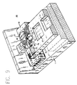
- FIG. 9 illustrates an alternative silicon-based optical subassembly 68 formed in accordance with the present invention.
- the signal ground plane is provided, using vias through the substrate, on top surface 13 of substrate 11.
- the high frequency signal connections to laser 40 are provided by a first connection 70 and a second connection 72.
- Connection 70 is attached to a first metallic strip 74, where strip 74 is subsequently attached to chip carrier 38.
- Second connection 72 is coupled by a series of vias (not shown) to a second metallic strip 76 disposed on the underside of substrate 11 (illustrated in phantom in FIG. 9).
- First metallic strip 74, silicon substrate 11 and second metallic strip 76 form a stripline to provide a high frequency interconnection between an external signal source (not shown) and laser 40.
- a thin film resistor 78 is located on chip carrier 38 in proximity to laser 40 to provide impedance matching of the laser to the stripline.
- a thorough description of an exemplary silicon-based high-frequency interconnection may be found in Serial No. 287,778, fled December 21, 1988, entitled "Silicon-Based Mounting Structure for Semiconductor Optical Devices", and assigned to the assignee of the present invention.
- a silicon substrate is processed to include a via in proximity to the laser so as to provide for attachment of the underlying metallic strip to the top-side laser contact. The use of such a via connection, in conjunction with the impedance matching resistor, provides for a relatively robust high frequency connection at data rates exceeding 2 Gb/s.
- optical filters such as wavelength-selective filters or dichroic filters may be placed in silicon submount openings and optically aligned with the associated active device(s).
- a single submount could be formed to include an array structure of active devices, with the necessary passive components appropriately disposed in the silicon submount.
- an optical subassembly of the present invention could be configured as a optical transceiver subassembly including an optical transmitting device, an optical receiving device and the required lensing and filtering components.
Landscapes
- Physics & Mathematics (AREA)
- General Physics & Mathematics (AREA)
- Optics & Photonics (AREA)
- Condensed Matter Physics & Semiconductors (AREA)
- Electromagnetism (AREA)
- Engineering & Computer Science (AREA)
- Microelectronics & Electronic Packaging (AREA)
- Optical Couplings Of Light Guides (AREA)
- Semiconductor Lasers (AREA)
- Light Guides In General And Applications Therefor (AREA)
Claims (24)
- Un sous-ensemble optique comprenant :
un ensemble de dispositifs optiques (34, 36, 40, 44) ;
un substrat en silicium (11) défini de façon à comprendre une surface supérieure principale (13), ce substrat en silicium comprenant un ensemble d'ouvertures (12, 20, 22, 30) formées dans sa surface supérieure, l'ensemble d'ouvertures étant prévues pour le placement de l'ensemble de dispositifs optiques et étant disposées de façon à établir un alignement optique entre eux ; et
un élément de support (par exemple 48, 50), disposé par rapport au substrat en silicium de façon à former une configuration en porte-à-faux avec ce dernier. - Un sous-ensemble optique défini dans la revendication 1, comprenant en outre au moins un dispositif optique actif (40).
- Un sous-ensemble optique défini dans la revendication 2, dans lequel le ou les dispositifs optiques actifs comprennent un laser.
- Un sous-ensemble optique défini dans la revendication 2, dans lequel le dispositif optique actif, ou chacun d'eux, est placé à l'intérieur d'une ouverture (30) dans la surface supérieure du substrat en silicium, à proximité de l'élément de support.
- Un sous-ensemble optique défini dans la revendication 2, dans lequel l'ensemble de dispositifs optiques comprend en outre un isolateur optique (44).
- Un sous-ensemble optique défini dans la revendication 5, dans lequel l'isolateur optique comprend
un composant optique d'isolateur placé à l'intérieur d'une ouverture dans la surface supérieure du substrat en silicium, de façon à être en alignement optique avec le dispositif optique actif ; et
un aimant permanent (52) disposé de façon à entourer le composant optique d'isolateur de manière à éviter un contact physique avec le substrat en silicium. - Un sous-ensemble optique défini dans la revendication 2, dans lequel l'ensemble de dispositifs optiques comprend en outre au moins un composant optique passif (34, 36).
- Un sous-ensemble optique défini dans la revendication 7, dans lequel le ou les composants optiques passifs comprennent
une première lentille (34) pour coupler vers un milieu de communication optique externe un signal optique qui sort du sous-ensemble optique ; et
une seconde lentille (36) couplée au dispositif optique actif pour collimater l'émission optique de ce dernier. - Un sous-ensemble optique défini dans la revendication 8, dans lequel le milieu de communication optique externe comprend une fibre optique (54).
- Un sous-ensemble optique défini dans la revendication 8, dans lequel
la première lentille consiste en une lentille à gradient d'indice de forme cylindrique, pour transformer un faisceau d'entrée collimaté en un faisceau de sortie focalisé ; et
la seconde lentille consiste en une lentille sphérique pour collimater le signal d'entrée optique qui lui est appliqué. - Un sous-ensemble optique défini dans la revendication 10, dans lequel le substrat en silicium comprend
une première ouverture (18) pour la première lentille, cette première ouverture ayant une forme relativement trapézordale d'une profondeur d₁ ; et
une seconde ouverture (20) pour la seconde lentille, cette seconde ouverture ayant une forme relativement pyramidale carrée d'une profondeur d₂. - Un sous-ensemble optique défini dans la revendication 11, dans lequel la profondeur d₁ est dans la plage d'environ 500-700 »m, et la profondeur d₂ est dans la plage d'environ 100-200 »m.
- Un sous-ensemble optique défini dans la revendication 2, dans lequel l'élément de support comprend un dispositif de refroidissement thermo-électrique.
- Un sous-ensemble optique défini dans la revendication 13, dans lequel le dispositif de refroidissement thermoélectrique est disposé par rapport au substrat en silicium de façon à établir un chemin de transfert thermique à travers le substrat en silicium, vers le dispositif actif.
- Un sous-ensemble optique défini dans la revendication 14, dans lequel l'ensemble de dispositifs optiques comprend en outre un isolateur optique comprenant un composant optique d'isolateur qui est placé à l'intérieur d'une ouverture dans la surface supérieure du substrat en silicium, et qui est disposé le long du chemin de transfert thermique entre le dispositif de refroidissement thermoélectrique et le substrat en silicium.
- Un sous-ensemble optique défini dans la revendication 2, dans lequel le dispositif optique actif, ou chacun d'eux, est disposé sur un support de puce optique (38), ce support de puce optique étant fixé sur la surface supérieure du substrat en silicium.
- Un sous-ensemble optique défini dans la revendication 16, dans lequel le support de puce est fixé à l'intérieur d'une ouverture formée dans la surface supérieure du substrat en silicium, la profondeur de l'ouverture étant telle que la région active du dispositif optique reste placée au-dessus de la surface supérieure du substrat en silicium.
- Un sous-ensemble optique défini dans la revendication 2, dans lequel les dispositifs actifs comprennent en outre à titre de second dispositif actif, un dispositif de contrôle de face arrière (46) qui est positionné de façon à intercepter le signal optique sortant par la face arrière du premier dispositif actif.
- Un sous-ensemble optique défini dans la revendication 1, dans lequel le substrat en silicium consiste en silicium d'orientation <100> , de façon que l'ensemble d'ouvertures comprennent des parois latérales allant en se rapprochant vers l'intérieur, d'orientation <111>.
- Un sous-ensemble optique comprenant
un dispositif optique à semiconducteurs actif (par exemple 40) ;
des moyens d'isolation (par exemple 44), pour empêcher que des signaux réfléchis ne retournent vers l'intérieur du dispositif optique à semiconducteurs actif ;
une première lentille (par exemple 34), disposée après les moyens d'isolation, pour focaliser l'émission de sortie des moyens d'isolation vers un milieu de guidage d'ondes optique couplé ;
une seconde lentille (par exemple 36), disposée entre le dispositif actif et les moyens d'isolation, pour collimater l'émission du dispositif actif vers l'entrée des moyens d'isolation ; et
un substrat en silicium (par exemple 11) comprenant un ensemble d'ouvertures (par exemple 12, 20, 22, 30) formées dans sa surface supérieure, pour le placement des moyens d'isolation et des première et seconde lentilles, l'ensemble d'ouvertures étant disposées de façon à assurer un alignement optique entre eux. - Un sous-ensemble optique défini dans la revendication 20, dans lequel les moyens d'isolation comprennent
un composant optique d'isolateur (42) placé dans une ouverture dans le substrat en silicium ; et
un aimant permanent (52) disposé de façon à entourer le substrat en silicium au voisinage des composants optiques d'isolateur ;
le sous-ensemble comprenant en outre
des moyens de support (48) fixés sur la face inférieure du substrat en silicium, de manière à procurer une configuration de sous-ensemble optique en porte-à-faux, dans laquelle un contact physique entre l'aimant permanent et le substrat en silicium est évité. - Un sous-ensemble optique défini dans la revendication 21, dans lequel les moyens de support comprennent un dispositif de refroidissement thermoélectrique qui est fixé à la face inférieure du substrat en silicium, au voisinage du dispositif optique à semiconducteurs actif et du composant optique d'isolateur.
- Un sous-ensemble optique défini dans la revendication 20, dans lequel
la première lentille consiste en une lentille GRIN cylindrique (34), placée dans une ouverture relativement pyramidale rectangulaire dans le substrat en silicium ; et
la seconde lentille consiste en une lentille sphérique (36), placée dans une ouverture relativement pyramidale carrée dans le substrat en silicium. - Un sous-ensemble optique défini dans la revendication 20, dans lequel le substrat en silicium est formé de façon à comprendre une ouverture (30) pour le placement d'un support de puce de dispositif actif.
Applications Claiming Priority (2)
| Application Number | Priority Date | Filing Date | Title |
|---|---|---|---|
| US548694 | 1990-07-05 | ||
| US07/548,694 US5113404A (en) | 1990-07-05 | 1990-07-05 | Silicon-based optical subassembly |
Publications (3)
| Publication Number | Publication Date |
|---|---|
| EP0465230A2 EP0465230A2 (fr) | 1992-01-08 |
| EP0465230A3 EP0465230A3 (en) | 1992-04-29 |
| EP0465230B1 true EP0465230B1 (fr) | 1995-05-03 |
Family
ID=24189997
Family Applications (1)
| Application Number | Title | Priority Date | Filing Date |
|---|---|---|---|
| EP91306016A Expired - Lifetime EP0465230B1 (fr) | 1990-07-05 | 1991-07-02 | Sous-ensemble à base de silicium |
Country Status (4)
| Country | Link |
|---|---|
| US (1) | US5113404A (fr) |
| EP (1) | EP0465230B1 (fr) |
| JP (2) | JP2846981B2 (fr) |
| DE (1) | DE69109378T2 (fr) |
Cited By (6)
| Publication number | Priority date | Publication date | Assignee | Title |
|---|---|---|---|---|
| US6771859B2 (en) | 2001-07-24 | 2004-08-03 | 3M Innovative Properties Company | Self-aligning optical micro-mechanical device package |
| US6792012B2 (en) | 2001-04-30 | 2004-09-14 | Jds Uniphase Corporation | Laser pump module with reduced tracking error |
| US6798954B2 (en) | 2001-07-24 | 2004-09-28 | 3M Innovative Properties Company | Packaged optical micro-mechanical device |
| US6834154B2 (en) | 2001-07-24 | 2004-12-21 | 3M Innovative Properties Co. | Tooling fixture for packaged optical micro-mechanical devices |
| US7288758B2 (en) | 1998-11-25 | 2007-10-30 | Rohm And Haas Electronic Materials Llc | Wafer-level optoelectronic device substrate |
| US8703603B2 (en) | 2003-09-15 | 2014-04-22 | Nuvotronics, Llc | Device package and methods for the fabrication and testing thereof |
Families Citing this family (66)
| Publication number | Priority date | Publication date | Assignee | Title |
|---|---|---|---|---|
| DE3925201A1 (de) * | 1989-07-29 | 1991-02-07 | Messerschmitt Boelkow Blohm | Optische bank zur halterung optischer, elektrischer u.a. komponenten |
| JP2976642B2 (ja) * | 1991-11-07 | 1999-11-10 | 日本電気株式会社 | 光結合回路 |
| US5181214A (en) * | 1991-11-18 | 1993-01-19 | Harmonic Lightwaves, Inc. | Temperature stable solid-state laser package |
| JP2763980B2 (ja) * | 1992-01-14 | 1998-06-11 | 富士通株式会社 | 光半導体モジュール |
| US5361272A (en) * | 1992-09-18 | 1994-11-01 | Stephen Krissman | Semiconductor architecture and application thereof |
| JPH06232504A (ja) * | 1993-01-29 | 1994-08-19 | Canon Inc | レーザ走査装置 |
| US5550088A (en) * | 1993-06-02 | 1996-08-27 | Lucent Technologies Inc. | Fabrication process for a self-aligned optical subassembly |
| JP2945246B2 (ja) * | 1993-06-23 | 1999-09-06 | 株式会社日立製作所 | 光素子モジュール |
| JPH0774343A (ja) * | 1993-08-31 | 1995-03-17 | Fujitsu Ltd | 集積化光装置及びその製造方法 |
| US5657151A (en) * | 1993-12-09 | 1997-08-12 | Lucent Technologies Inc. | Polarization scrambler/modulator |
| FR2714740B1 (fr) * | 1994-01-03 | 1996-02-02 | Alcatel Nv | Ensemble d'isolation optique et module d'émission optique comportant cet ensemble. |
| USD354275S (en) | 1994-04-08 | 1995-01-10 | Sgs-Thomson Microelectronics, Inc. | Low-profile detachable integrated circuit module |
| USD354274S (en) | 1994-04-08 | 1995-01-10 | SGS - Thomson Microelectronics, Inc. | Low-profile detachable integrated circuit module |
| DE4422322C1 (de) * | 1994-06-27 | 1995-09-14 | Ant Nachrichtentech | Lasermodul |
| DE4431285C1 (de) * | 1994-09-02 | 1995-12-07 | Ant Nachrichtentech | Lasermodul |
| HUT76920A (hu) * | 1994-09-15 | 1998-01-28 | Robert Bosch Gmbh. | Lézermodul |
| JP3439275B2 (ja) * | 1994-11-25 | 2003-08-25 | エヌイーシートーキン株式会社 | 光アイソレータの製造方法 |
| JP3658426B2 (ja) * | 1995-01-23 | 2005-06-08 | 株式会社日立製作所 | 光半導体装置 |
| US5602860A (en) * | 1995-04-19 | 1997-02-11 | Optelecom, Inc. | Laser thermal control using thermoelectric cooler |
| US6389582B1 (en) * | 1995-12-21 | 2002-05-14 | John Valainis | Thermal driven placement |
| DE19605726A1 (de) * | 1996-02-16 | 1997-08-21 | Sel Alcatel Ag | Anordnung zur optischen Ankopplung einer Monitordiode an eine Laserdiode |
| US5737349A (en) * | 1996-05-22 | 1998-04-07 | Lucent Technologies Inc. | Optical isolator and alignment method |
| WO1998047032A2 (fr) * | 1997-04-11 | 1998-10-22 | Digital Optics Corporation | Systeme de transmission optique a batonnet optique recouvert de motifs tridimensionnels et des structures associees |
| US5996376A (en) * | 1997-04-11 | 1999-12-07 | Digital Optics Corporation | Methods of forming optical rods including three-dimensional patterns on end faces thereof |
| US5930429A (en) * | 1997-07-01 | 1999-07-27 | Hewlett-Packard Company | Micro-photonics module integrated on a single substrate |
| US6072815A (en) * | 1998-02-27 | 2000-06-06 | Litton Systems, Inc. | Microlaser submount assembly and associates packaging method |
| US6240113B1 (en) | 1998-02-27 | 2001-05-29 | Litton Systems, Inc. | Microlaser-based electro-optic system and associated fabrication method |
| US6218641B1 (en) | 1998-04-22 | 2001-04-17 | Lucent Technologies, Inc. | Method for compensating stress induced in an optical component |
| US6221739B1 (en) | 1998-08-20 | 2001-04-24 | Vladimir A. Gorelik | Method for bonding single crystal membranes to a curved surface |
| EP1788416B1 (fr) * | 1998-09-24 | 2008-03-05 | LG Cable & Machinery Ltd. | Procédé de fabrication de puce à diode laser |
| WO2000064018A1 (fr) | 1999-04-20 | 2000-10-26 | The Furukawa Electric Co., Ltd. | Module laser a semi-conducteur |
| US6213651B1 (en) | 1999-05-26 | 2001-04-10 | E20 Communications, Inc. | Method and apparatus for vertical board construction of fiber optic transmitters, receivers and transceivers |
| US6901221B1 (en) | 1999-05-27 | 2005-05-31 | Jds Uniphase Corporation | Method and apparatus for improved optical elements for vertical PCB fiber optic modules |
| US6136411A (en) * | 1999-07-29 | 2000-10-24 | Lucent Technologies, Inc. | Angularly self-aligned optical subassembly |
| JP4540155B2 (ja) * | 1999-10-28 | 2010-09-08 | 京セラ株式会社 | 光アイソレータ |
| JP3914670B2 (ja) * | 1999-11-18 | 2007-05-16 | パイオニア株式会社 | 半導体モジュール及び半導体モジュールの半導体レーザ素子の取り付け方法 |
| JP2003107295A (ja) * | 2001-09-28 | 2003-04-09 | Opnext Japan Inc | 光伝送モジュール |
| RU2201024C2 (ru) * | 2001-01-16 | 2003-03-20 | Федеральное государственное унитарное предприятие Научно-исследовательский институт "Полюс" | Оптический передающий модуль |
| RU2201025C2 (ru) * | 2001-01-16 | 2003-03-20 | Федеральное государственное унитарное предприятие Научно-исследовательский институт "Полюс" | Способ изготовления оптического передающего модуля |
| US6546173B2 (en) * | 2001-02-20 | 2003-04-08 | Avanti Optics Corporation | Optical module |
| US6443631B1 (en) | 2001-02-20 | 2002-09-03 | Avanti Optics Corporation | Optical module with solder bond |
| US6546172B2 (en) | 2001-02-20 | 2003-04-08 | Avanti Optics Corporation | Optical device |
| US20040212802A1 (en) * | 2001-02-20 | 2004-10-28 | Case Steven K. | Optical device with alignment compensation |
| US6956999B2 (en) | 2001-02-20 | 2005-10-18 | Cyberoptics Corporation | Optical device |
| DE10117020C2 (de) | 2001-04-05 | 2003-05-08 | Unique M O D E Ag | Optisches oder optoelektronisches Modul |
| JPWO2002089274A1 (ja) * | 2001-04-25 | 2004-08-19 | 住友電気工業株式会社 | 光通信装置 |
| US6792008B2 (en) * | 2001-04-30 | 2004-09-14 | Jds Uniphase Corporation | Tracking error suppression and method of reducing tracking error |
| US6748137B2 (en) | 2001-04-30 | 2004-06-08 | Jds Uniphase Corporation | Lensed optical fiber |
| US6762119B2 (en) * | 2001-06-20 | 2004-07-13 | International Bussiness Machines Corporation | Method of preventing solder wetting in an optical device using diffusion of Cr |
| US20030012508A1 (en) * | 2001-06-22 | 2003-01-16 | Bookham Technology, Plc. | Fibre support |
| US6845121B2 (en) * | 2002-06-15 | 2005-01-18 | Intel Corporation | Optical isolator apparatus and methods |
| US6865321B2 (en) * | 2002-07-31 | 2005-03-08 | Agilent Technologies, Inc. | Optical systems and methods using coupling fixtures for aligning optical elements with planar waveguides |
| US20040264870A1 (en) * | 2002-08-20 | 2004-12-30 | Skunes Timothy A. | Optical alignment mount with height adjustment |
| JP3896951B2 (ja) * | 2002-11-13 | 2007-03-22 | 松下電器産業株式会社 | 光通信用送受光モジュール |
| JP2004179273A (ja) * | 2002-11-26 | 2004-06-24 | Nec Corp | 半導体レーザチップ部品及びこれを用いた半導体レーザモジュール |
| EP1680843A4 (fr) * | 2003-10-20 | 2009-05-06 | Binoptics Corp | Dispositif photonique a emission et a reception de surface |
| US7598527B2 (en) * | 2004-01-20 | 2009-10-06 | Binoptics Corporation | Monitoring photodetector for integrated photonic devices |
| US20060274797A1 (en) * | 2005-06-07 | 2006-12-07 | Kigre, Inc. | Method for cooling semiconductor diodes and light emitting diodes |
| GB0904247D0 (en) * | 2009-03-12 | 2009-04-22 | Cip Technologies Ltd | Hybrid integrated tuneable laser |
| TW201108332A (en) * | 2009-08-27 | 2011-03-01 | Univ Nat Central | Package base structure and related manufacturing method |
| JP5693888B2 (ja) * | 2010-07-28 | 2015-04-01 | 住友電工デバイス・イノベーション株式会社 | 光デバイスおよびその製造方法 |
| JP6136315B2 (ja) * | 2013-02-04 | 2017-05-31 | 住友電気工業株式会社 | 光送信モジュールの製造方法 |
| WO2018045597A1 (fr) * | 2016-09-12 | 2018-03-15 | Xiamen Chaoxuan Photoelectric Technology Co., Ltd. | Système et dispositif à éclairage par réseau laser |
| US10107975B1 (en) | 2017-11-13 | 2018-10-23 | Denselight Semiconductors Pte. Ltd. | Optoelectronic assembly for optical coupling |
| US10319654B1 (en) | 2017-12-01 | 2019-06-11 | Cubic Corporation | Integrated chip scale packages |
| US10374386B1 (en) * | 2018-06-07 | 2019-08-06 | Finisar Corporation | Chip on carrier |
Family Cites Families (15)
| Publication number | Priority date | Publication date | Assignee | Title |
|---|---|---|---|---|
| US4301429A (en) * | 1979-06-07 | 1981-11-17 | Raytheon Company | Microwave diode with high resistance layer |
| JPS5621107A (en) * | 1979-07-27 | 1981-02-27 | Nec Corp | Light isolator coupling device |
| JPS577989A (en) * | 1980-06-17 | 1982-01-16 | Matsushita Electric Ind Co Ltd | Mount for semiconductor laser |
| JPS5776509A (en) * | 1980-10-30 | 1982-05-13 | Nippon Sheet Glass Co Ltd | Optical fiber-lens coupler and its manufacture |
| JPS60412A (ja) * | 1983-06-17 | 1985-01-05 | Fujitsu Ltd | 2入力光受光装置 |
| US4686678A (en) * | 1984-03-27 | 1987-08-11 | Nec Corporation | Semiconductor laser apparatus with isolator |
| JPS6155792A (ja) * | 1984-08-28 | 1986-03-20 | Canon Inc | 読取記録装置 |
| JPS6170516A (ja) * | 1984-09-14 | 1986-04-11 | Hitachi Ltd | 光アイソレ−タ付半導体レ−ザモジユ−ル |
| JPS6242109A (ja) * | 1985-08-20 | 1987-02-24 | Oki Electric Ind Co Ltd | 光半導体素子と光フアイバの結合器 |
| US4761788A (en) * | 1985-10-28 | 1988-08-02 | American Telephone And Telegraph Company | Stripline mount for semiconductor lasers |
| US4779946A (en) * | 1986-02-14 | 1988-10-25 | American Telephone And Telegraph Company, At&T Bell Laboratories | Microminiature optical assembly |
| JPS6439671U (fr) * | 1987-09-01 | 1989-03-09 | ||
| US4890895A (en) * | 1987-11-13 | 1990-01-02 | Kopin Corporation | Optoelectronic interconnections for III-V devices on silicon |
| US4897711A (en) * | 1988-03-03 | 1990-01-30 | American Telephone And Telegraph Company | Subassembly for optoelectronic devices |
| US4945400A (en) * | 1988-03-03 | 1990-07-31 | At&T Bell Laboratories | Subassembly for optoelectronic devices |
-
1990
- 1990-07-05 US US07/548,694 patent/US5113404A/en not_active Expired - Lifetime
-
1991
- 1991-07-02 DE DE69109378T patent/DE69109378T2/de not_active Expired - Lifetime
- 1991-07-02 EP EP91306016A patent/EP0465230B1/fr not_active Expired - Lifetime
- 1991-07-05 JP JP3191252A patent/JP2846981B2/ja not_active Expired - Lifetime
-
1998
- 1998-08-21 JP JP10235214A patent/JPH11174284A/ja active Pending
Cited By (10)
| Publication number | Priority date | Publication date | Assignee | Title |
|---|---|---|---|---|
| US7288758B2 (en) | 1998-11-25 | 2007-10-30 | Rohm And Haas Electronic Materials Llc | Wafer-level optoelectronic device substrate |
| US7288756B2 (en) | 1998-11-25 | 2007-10-30 | Rohm And Haas Electronic Materials Llc | Optoelectronic component having passively aligned optoelectronic device |
| US7291833B2 (en) | 1998-11-25 | 2007-11-06 | Rohm And Haas Electronic Materials Llc | Optoelectronic component |
| US7348550B2 (en) | 1998-11-25 | 2008-03-25 | Rohm And Haas Electronic Materials Llc | Optoelectronic component with front to side surface electrical conductor |
| US7355166B2 (en) | 1998-11-25 | 2008-04-08 | Rohm And Haas Electronic Materials Llc | Optoelectronic component having electrical connection and formation method thereof |
| US6792012B2 (en) | 2001-04-30 | 2004-09-14 | Jds Uniphase Corporation | Laser pump module with reduced tracking error |
| US6771859B2 (en) | 2001-07-24 | 2004-08-03 | 3M Innovative Properties Company | Self-aligning optical micro-mechanical device package |
| US6798954B2 (en) | 2001-07-24 | 2004-09-28 | 3M Innovative Properties Company | Packaged optical micro-mechanical device |
| US6834154B2 (en) | 2001-07-24 | 2004-12-21 | 3M Innovative Properties Co. | Tooling fixture for packaged optical micro-mechanical devices |
| US8703603B2 (en) | 2003-09-15 | 2014-04-22 | Nuvotronics, Llc | Device package and methods for the fabrication and testing thereof |
Also Published As
| Publication number | Publication date |
|---|---|
| DE69109378D1 (de) | 1995-06-08 |
| DE69109378T2 (de) | 1996-01-04 |
| US5113404A (en) | 1992-05-12 |
| EP0465230A3 (en) | 1992-04-29 |
| JPH11174284A (ja) | 1999-07-02 |
| JP2846981B2 (ja) | 1999-01-13 |
| JPH04270307A (ja) | 1992-09-25 |
| EP0465230A2 (fr) | 1992-01-08 |
Similar Documents
| Publication | Publication Date | Title |
|---|---|---|
| US5113404A (en) | Silicon-based optical subassembly | |
| US5264392A (en) | Fabrication technique for silicon-based optical subassemblies | |
| JP2507644B2 (ja) | 光 源 | |
| US9343450B2 (en) | Wafer scale packaging platform for transceivers | |
| US9329349B2 (en) | Integrated optical cooling core for optoelectronic interconnect modules | |
| US6965714B2 (en) | Integrated aspheric optical coupler for RF planarized automatic photonics packaging | |
| EP0415094A2 (fr) | Boîte d'alignement à fibres multiples pour composants opto-électroniques avec des facettes inclinées | |
| US20060239605A1 (en) | Optical coupling to IC chip | |
| JPH0611632A (ja) | 自動整合光ファイバ・リンク | |
| JPH10282364A (ja) | 光学デバイスの組立体 | |
| JPH06196816A (ja) | レンズ付きレーザダイオードおよびその製造方法 | |
| US5771323A (en) | Micro-photonics module | |
| JPH1123914A (ja) | 光素子と光ファイバとの固定構造 | |
| EP3994777B1 (fr) | Moteur laser supportant de multiples sources laser | |
| JPH07199006A (ja) | 光サブアセンブリ及び光モジュール | |
| US6249627B1 (en) | Arrangement for self-aligning optical fibers to an array of surface emitting lasers | |
| US9651749B1 (en) | Interposer with opaque substrate | |
| US4944569A (en) | Multi-fiber alignment package for optoelectronic components | |
| US5224184A (en) | Optical multi-chip interconnect | |
| US5930429A (en) | Micro-photonics module integrated on a single substrate | |
| JP2002341189A (ja) | 光モジュール | |
| Armiento | Hybrid optoelectronic integration of transmitter arrays on silicon waferboard | |
| JPH0667069A (ja) | 光半導体装置 | |
| JP2002062458A (ja) | 光モジュールおよびその組立方法、光モジュールを用いた映像表示装置 | |
| JPH06174979A (ja) | 小型光モジュール |
Legal Events
| Date | Code | Title | Description |
|---|---|---|---|
| PUAI | Public reference made under article 153(3) epc to a published international application that has entered the european phase |
Free format text: ORIGINAL CODE: 0009012 |
|
| AK | Designated contracting states |
Kind code of ref document: A2 Designated state(s): DE FR GB |
|
| PUAL | Search report despatched |
Free format text: ORIGINAL CODE: 0009013 |
|
| AK | Designated contracting states |
Kind code of ref document: A3 Designated state(s): DE FR GB |
|
| 17P | Request for examination filed |
Effective date: 19921015 |
|
| RAP3 | Party data changed (applicant data changed or rights of an application transferred) |
Owner name: AT&T CORP. |
|
| 17Q | First examination report despatched |
Effective date: 19940928 |
|
| GRAA | (expected) grant |
Free format text: ORIGINAL CODE: 0009210 |
|
| AK | Designated contracting states |
Kind code of ref document: B1 Designated state(s): DE FR GB |
|
| REF | Corresponds to: |
Ref document number: 69109378 Country of ref document: DE Date of ref document: 19950608 |
|
| ET | Fr: translation filed | ||
| PLBE | No opposition filed within time limit |
Free format text: ORIGINAL CODE: 0009261 |
|
| STAA | Information on the status of an ep patent application or granted ep patent |
Free format text: STATUS: NO OPPOSITION FILED WITHIN TIME LIMIT |
|
| 26N | No opposition filed | ||
| PGFP | Annual fee paid to national office [announced via postgrant information from national office to epo] |
Ref country code: FR Payment date: 20010625 Year of fee payment: 11 |
|
| REG | Reference to a national code |
Ref country code: GB Ref legal event code: IF02 |
|
| PG25 | Lapsed in a contracting state [announced via postgrant information from national office to epo] |
Ref country code: FR Free format text: LAPSE BECAUSE OF NON-PAYMENT OF DUE FEES Effective date: 20030331 |
|
| REG | Reference to a national code |
Ref country code: FR Ref legal event code: ST |
|
| PGFP | Annual fee paid to national office [announced via postgrant information from national office to epo] |
Ref country code: DE Payment date: 20100723 Year of fee payment: 20 |
|
| PGFP | Annual fee paid to national office [announced via postgrant information from national office to epo] |
Ref country code: GB Payment date: 20100722 Year of fee payment: 20 |
|
| REG | Reference to a national code |
Ref country code: DE Ref legal event code: R071 Ref document number: 69109378 Country of ref document: DE |
|
| REG | Reference to a national code |
Ref country code: DE Ref legal event code: R071 Ref document number: 69109378 Country of ref document: DE |
|
| REG | Reference to a national code |
Ref country code: GB Ref legal event code: PE20 Expiry date: 20110701 |
|
| PG25 | Lapsed in a contracting state [announced via postgrant information from national office to epo] |
Ref country code: GB Free format text: LAPSE BECAUSE OF EXPIRATION OF PROTECTION Effective date: 20110701 |
|
| PG25 | Lapsed in a contracting state [announced via postgrant information from national office to epo] |
Ref country code: DE Free format text: LAPSE BECAUSE OF EXPIRATION OF PROTECTION Effective date: 20110703 |